
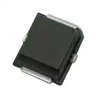


MMRF1014NT1
RF FET Transistor, 68 V, 2 GHz, 1 MHz, PLD-1.5
- Manufacturer: NXP
- Product type: RF FETs
- Drain Source Voltage Vds:68V; Continuous Drain Current Id:-; Power Dissipation Pd:-; Operating Frequency Min:2GHz; Operating Frequency Max:1MHz; RF Transistor Case:PLD-1.5; No. of Pins:2P
- MSL: MSL 3 - 168 hours
- SVHC: No SVHC (27-Jun-2024)
- No. of Pins: 2Pins
- Channel Type: N Channel
- Product Range: MMRF1014N
- Power Dissipation: -
- Transistor Mounting: Surface Mount
- Transistor Case Style: PLD-1.5
- Operating Frequency Max: 1MHz
- Operating Frequency Min: 2GHz
- Drain Source Voltage Vds: 68V
- Operating Temperature Max: 150°C
- Continuous Drain Current Id: -
| Delivery and price | |
|---|---|
| Units per pack | 250 |
| Price | 10.21 € |
| Current stock | 10+ |
| Lead time | 30 days |
**Freescale Semiconductor** Technical Data
Document Number: MMRF1014N Rev. 0, 7/2014
## **RF Power LDMOS Transistor**
## N--Channel Enhancement--Mode Lateral MOSFET
Designed for Class A or Class AB power amplifier applications with frequencies up to 2000 MHz. Suitable for analog and digital modulation and multicarrier amplifier applications.
- Typical Two--Tone Performance @ 1960 MHz, 28 Vdc, IDQ = 50 mA, Pout = 4 W PEP Power Gain — 18 dB
- Drain Efficiency — 33% IMD — --34 dBc
## **MMRF1014NT1**
**1--2000 MHz, 4 W, 28 V CLASS A/AB RF POWER MOSFET**
- Typical Two--Tone Performance @ 900 MHz, 28 Vdc, IDQ = 50 mA, Pout = 4 W PEP
- Power Gain — 19 dB Drain Efficiency — 33% IMD — --39 dBc
- Capable of Handling 5:1 VSWR @ 28 Vdc, 1960 MHz, 4 W CW Output Power
- **Features**
- Characterized with Series Equivalent Large--Signal Impedance Parameters
- On--Chip RF Feedback for Broadband Stability
**==> picture [35 x 17] intentionally omitted <==**
**----- Start of picture text -----**<br>
PLD--1.5<br>PLASTIC<br>**----- End of picture text -----**<br>
- Integrated ESD Protection
- In Tape and Reel. T1 Suffix = 1,000 Units,16 mm Tape Width, 7--inch Reel.
**==> picture [100 x 7] intentionally omitted <==**
**----- Start of picture text -----**<br>
Gate Drain<br>**----- End of picture text -----**<br>
Note: The center pad on the backside of the package is the source terminal for the transistor.
## **Figure 1. Pin Connections**
## **Table 1. Maximum Ratings**
|**Table 1. Maximum Ratings**||||
|---|---|---|---|
|**Rating**|**Symbol**|**Value**|**Unit**|
|Drain--Source Voltage|VDSS|--0.5, +68|Vdc|
|Gate--Source Voltage|VGS|--0.5, +12|Vdc|
|Storage Temperature Range|Tstg|-- 65 to +150|C|
|Operating Junction Temperature|TJ|150|C|
|**Table 2. Thermal Characteristics**||||
|**Characteristic**|**Symbol**|**Value (1,2)**|**Unit**|
|Thermal Resistance, Junction to Case|RJC||C/W|
|Case Temperature 76C, 4 W PEP, Two--Tone||8.8||
|Case Temperature 79C, 4 W CW||8.5||
|**Table 3. ESD Protection Characteristics**||||
|**Test Methodology**||**Class**||
|Human Body Model (per JESD22--A114)||1C||
|Machine Model (per EIA/JESD22--A115)||A||
|Charge Device Model (per JESD22--C101)||IV||
## **Table 2. Thermal Characteristics**
## **Table 3. ESD Protection Characteristics**
1. MTTF calculator available at http://www.freescale.com/rf. Select Software & Tools/Development Tools/Calculators to access MTTF calculators by product.
2. Refer to AN1955, _Thermal Measurement Methodology of RF Power Amplifiers._ Go to http://www.freescale.com/rf. Select Documentation/Application Notes -- AN1955.
**MMRF1014NT1** ~~=freescale~~
Freescale Semiconductor, Inc., 2014. All rights reserved.
**MMRF1014NT1**
RF Device Data Freescale Semiconductor, Inc.
1
## **Table 4. Moisture Sensitivity Level**
|**Test Methodology**<br>**Rating**<br>**Package Peak Temperature**<br>**Unit**|
|---|
|Per JESD22--A113, IPC/JEDEC J--STD--020<br>3<br>260<br>C|
|**Table 5. Electrical Characteristics** (TA= 25C unless otherwise noted)|
|**Characteristic**<br>**Symbol**<br>**Min**<br>**Typ**<br>**Max**<br>**Unit**|
|**Off Characteristics**|
|Zero Gate Voltage Drain Leakage Current<br>(VDS= 68 Vdc, VGS= 0 Vdc)<br>IDSS<br>—<br>—<br>10<br>Adc<br>Zero Gate Voltage Drain Leakage Current<br>(VDS= 28 Vdc, VGS= 0 Vdc)<br>IDSS<br>—<br>—<br>10<br>Adc<br>Gate--Source Leakage Current<br>(VGS= 5 Vdc, VDS= 0 Vdc)<br>IGSS<br>—<br>—<br>500<br>nAdc<br>~~re~~|
|**On Characteristics**|
|Gate Threshold Voltage<br>(VDS= 10 Vdc, ID= 50 mAdc)<br>VGS(th)<br>1.2<br>2<br>2.7<br>Vdc<br>Gate Quiescent Voltage<br>(VDS= 28 Vdc, ID= 50 mAdc)<br>VGS(Q)<br>—<br>2.7<br>—<br>Vdc<br>Fixture Gate Quiescent Voltage (1)<br>(VDD= 28 Vdc, ID= 50 mAdc, Measured in Functional Test)<br>VGG(Q)<br>2.2<br>3<br>4.2<br>Vdc<br>Drain--Source On--Voltage<br>(VGS= 10 Vdc, ID= 50 mAdc)<br>VDS(on)<br>—<br>0.27<br>0.37<br>Vdc<br>~~EE~~|
|**Dynamic Characteristics**|
|Reverse Transfer Capacitance<br>(VDS= 28 Vdc30 mV(rms)ac @ 1 MHz, VGS= 0 Vdc)<br>Crss<br>—<br>21<br>—<br>pF<br>Output Capacitance<br>(VDS= 28 Vdc30 mV(rms)ac @ 1 MHz, VGS= 0 Vdc)<br>Coss<br>—<br>25<br>—<br>pF<br>Input Capacitance<br>(VDS= 28 Vdc, VGS= 0 Vdc30 mV(rms)ac @ 1 MHz)<br>Ciss<br>—<br>30<br>—<br>pF<br>~~BS~~|
|**Functional Tests**(In Freescale Test Fixture, 50 ohm system) VDD= 28 Vdc, IDQ= 50 mA, Pout= 4 W PEP, f1 = 1960 MHz,|
|f2 = 1960.1 MHz, Two--Tone Test|
|Power Gain<br>Gps<br>16.5<br>18<br>20<br>dB<br>Drain Efficiency<br>D<br>28<br>33<br>—<br>%<br>Intermodulation Distortion<br>IMD<br>—<br>--34<br>--28<br>dBc<br>Input Return Loss<br>IRL<br>—<br>--12<br>--10<br>dB<br>**Typical Performance**(In Freescale 900 MHz Demo Board, 50 ohm system) VDD= 28 Vdc, IDQ= 50 mA, Pout= 4 W PEP,<br>f = 900 MHz, Two--Tone Test, 100 kHz Tone Spacing<br>Power Gain<br>Gps<br>—<br>19<br>—<br>dB<br>Drain Efficiency<br>D<br>—<br>33<br>—<br>%<br>Intermodulation Distortion<br>IMD<br>—<br>--39<br>—<br>dBc<br>Input Return Loss<br>IRL<br>—<br>--12<br>—<br>dB<br>1. VGG= 11/10x VGS(Q). Parameter measured on Freescale Test Fixture, due to resistive divider network on the board.<br>Refer to Test Circuit Schematic.<br>~~===~~<br>~~=EEEEE~~|
**MMRF1014NT1**
RF Device Data Freescale Semiconductor, Inc.
2
**==> picture [434 x 258] intentionally omitted <==**
**----- Start of picture text -----**<br>
EE — — — — — — — — EEE<br>R1<br>VBIAS VSUPPLY<br>+<br>R2<br>C8 C1 C7 Z5 C3 C4 C5<br>Z10<br>RF<br>OUTPUT<br>R3 Z6 Z7 Z8 Z9<br>RF<br>INPUT<br>Z1 Z2 Z3 Z4<br>C6<br>C2<br>DUT<br>on Z1 0.054 x 0.430 Microstrip Z7 0.210 x 1.220 Microstrip<br>Z2 0.054 x 0.137 Microstrip Z8 0.054 x 0.680 Microstrip<br>Z3 0.580 x 0.420 Microstrip Z9 0.054 x 0.260 Microstrip<br>Z4 0.580 x 0.100 Microstrip Z10 0.025 x 0.930 Microstrip<br>Z5 0.025 x 0.680 Microstrip PCB Arlon CuClad 250GX--0300--55--22, 0.020, r = 2.5<br>Z6 0.210 x 0.100 Microstrip<br>**----- End of picture text -----**<br>
**Figure 2. MMRF1014NT1 Test Circuit Schematic**
**Table 6. MMRF1014NT1 Test Circuit Component Designations and Values**
|**Part**|**Description**|**Part Number**|**Manufacturer**|
|---|---|---|---|
|C1|100 nF Chip Capacitor|CDR33BX104AKYS|Kemet|
|C2, C3, C6, C7|9.1 pF Chip Capacitors|ATC100B9R1CT500XT|ATC|
|C4, C5|10F, 50 V Chip Capacitors|GRM55DR61H106KA88B|Murata|
|C8|10F, 35 V Tantalum Chip Capacitor|T490D106K035AT|Kemet|
|R1|1 k, 1/4 W Chip Resistor|CRCW12061001FKEA|Vishay|
|R2|10 k, 1/4 W Chip Resistor|CRCW12061002FKEA|Vishay|
|R3|10, 1/4 W ChipResistor|CRCW120610R0FKEA|Vishay|
**MMRF1014NT1**
RF Device Data Freescale Semiconductor, Inc.
3
**==> picture [444 x 135] intentionally omitted <==**
**----- Start of picture text -----**<br>
25<br>lbP0000000000000 00000000000000000000000 ° ° ° °° °00000000000 00000° ° o Oo oO °0 00000000000000000000000000000000004<br>P<br>loeC —— =<br>b o0000000004 boO0R9000089000000000000 000000000 , 90 0.22900000000000000000000000000 °<br>—_b o ne ( THESBe 4 L__] °° o}° ee fed |_|<br>bbob oo Ll C8 R1 R2 C1 C7 °°° °°° C3 K—} C4 /——J C5<br>b o ° a<br>0<br>b 0 9 °<br>bobo é& loo<br>bo ° °<br>bo<br>R3 Fi RENS °<br>C2 C6<br>**----- End of picture text -----**<br>
**Figure 3. MMRF1014NT1 Test Circuit Component Layout**
**MMRF1014NT1**
RF Device Data Freescale Semiconductor, Inc.
4
**TYPICAL CHARACTERISTICS**
**==> picture [497 x 646] intentionally omitted <==**
**----- Start of picture text -----**<br>
18.4 34<br>18.2 ow 33<br>D<br>18 32<br>17.8 anna 31<br>Gps<br>17.6 30<br>VDD = 28 Vdc, Pout = 2 W (Avg.)<br>17.4 — IDQ = 50 mA, 100 kHz Tone Spacing —_ --30 --8<br>17.2 Soa = --31 --12<br>17 IRL --32 --16<br>16.8 eea --33 --20<br>16.6 --34 --24<br>IM3<br>16.4 aee ee ee ee ee --35 --28<br>1930 1940 1950 1960 1970 1980 1990<br>f, FREQUENCY (MHz)<br>Figure 4. Two--Tone Wideband Performance<br>@ Pout = 2 Watts Avg.<br>20 --10<br>IDQ = 75 mADQ = 75 mA = 75 mA VDD = 28 Vdc, IDQ = 50 mADD = 28 Vdc, IDQ = 50 mA = 28 Vdc, IDQ = 50 mADQ = 50 mA = 50 mA<br>--20 f1 = 1960 MHz, f2 = 1960.1 MHz<br>19<br>Two--Tone Measurements<br>62.5 mA<br>r eaa l SUTT III I --30 pF<br>18 err ie AE EY<br>50 mA<br>--40<br>oss PE TUIN L IE Aa<br>17<br>37.5 mA 3rd Order<br>--50<br>16<br>--60<br>25 mA R T)) eet 5th Order ear th<br>15 VDD = 28 VdcDD = 28 Vdc = 28 Vdc<br>f1 = 1960 MHz, f2 = 1960.1 MHz --70<br>Two--Tone Measurements 7th Order<br>14 allii l a mMt|Mt|| --80 a i ann onl A TT<br>0.01 0.1 1 10 20 0.01 0.1 1<br>Pout, OUTPUT POWER (WATTS) PEPout, OUTPUT POWER (WATTS) PEP, OUTPUT POWER (WATTS) PEP Pout, OUTPUT POWER (WATTS) PEPout, OUTPUT POWER (WATTS) PEP, OUTPUT POWER (WATTS) PEP<br>Figure 5. Two--Tone Power Gain versus Figure 6. Intermodulation Distortion Products<br>Output Power versus Output Power<br>--25 47<br>VDD = 28 Vdc, Pout = 2 W (Avg.), IDQ = 50 mA P6dB = 38.73 dBm (7.465 W) Ideal<br>--30 (f1 + f2)/2 = Center Frequency of 1960 MHz 45<br>--35 Py 43 e rt P3dB = 38.22 dBm (6.637 W) yy<br>at l | ie OO ei<br>3rd Order<br>--40 EIT a 41 er<br>TE A HEE P1dB = 37.61 dBm (5.768 W) EC<br>--45 A 39 ER eR<br>A Pe<br>Actual<br>--50 5th Order 37<br>Sane ee emstie Ol HES aS ge BE<br>VDD = 28 Vdc, IDQ = 50 mA<br>--55 35 Pulsed CW, 8 sec(on), 1 msec(off)<br>7th Order<br>f = 1960 MHz<br>--60 nealA 33 [aDaan a<br>0.1 1 10 100 14 16 18 20 22 24 26<br>TWO--TONE SPACING (MHz) Pin, INPUT POWER (dBm)<br>Figure 7. Intermodulation Distortion Products Figure 8. Pulsed CW Output Power versus<br>versus Tone Spacing Input Power<br>, DRAIN<br>D<br><br>EFFICIENCY (%)<br>, POWER GAIN (dB)<br>ps<br>G<br>IM3 (dBc)<br>IRL, INPUT RETURN LOSS (dB)<br>, POWER GAIN (dB)<br>ps<br>G<br>IMD, INTERMODULATION DISTORTION (dBc)<br>, OUTPUT POWER (dBm)<br>out<br>P<br>IMD, INTERMODULATION DISTORTION (dBc)<br>**----- End of picture text -----**<br>
**==> picture [499 x 199] intentionally omitted <==**
**----- Start of picture text -----**<br>
20 --10<br>IDQ = 75 mADQ = 75 mA = 75 mA VDD = 28 Vdc, IDQ = 50 mADD = 28 Vdc, IDQ = 50 mA = 28 Vdc, IDQ = 50 mADQ = 50 mA = 50 mA<br>--20 f1 = 1960 MHz, f2 = 1960.1 MHz<br>19<br>Two--Tone Measurements<br>62.5 mA<br>r eaa l SUTT III I --30 pF<br>18 err ie AE EY<br>50 mA<br>--40<br>oss PE TUIN L IE Aa<br>17<br>37.5 mA 3rd Order<br>--50<br>16<br>--60<br>25 mA R T)) eet 5th Order ear th<br>15 VDD = 28 VdcDD = 28 Vdc = 28 Vdc<br>f1 = 1960 MHz, f2 = 1960.1 MHz --70<br>Two--Tone Measurements 7th Order<br>14 allii l a mMt|Mt|| --80 a i ann onl A TT<br>0.01 0.1 1 10 20 0.01 0.1 1 10<br>Pout, OUTPUT POWER (WATTS) PEPout, OUTPUT POWER (WATTS) PEP, OUTPUT POWER (WATTS) PEP Pout, OUTPUT POWER (WATTS) PEPout, OUTPUT POWER (WATTS) PEP, OUTPUT POWER (WATTS) PEP<br>Figure 5. Two--Tone Power Gain versus Figure 6. Intermodulation Distortion Products<br>Output Power versus Output Power<br>, POWER GAIN (dB)<br>ps<br>G<br>IMD, INTERMODULATION DISTORTION (dBc)<br>**----- End of picture text -----**<br>
**MMRF1014NT1**
RF Device Data Freescale Semiconductor, Inc.
5
**TYPICAL CHARACTERISTICS**
**==> picture [503 x 637] intentionally omitted <==**
**----- Start of picture text -----**<br>
50 --20<br>VDD = 28 Vdc, IDQ = 50 mA<br>f = 1960 MHz, N--CDMA IS--95 (Pilot, Sync,<br>40 Paging, Traffic Codes 8 Through 13) --30<br>30 ey --40<br>20 CT Gps Pill --50<br>A T<br>10 ACPR --60<br>TM D eT ta<br>0 ET E --70<br>LUTE<br>0.01 0.1 1 10<br>Pout, OUTPUT POWER (WATTS) AVG.<br>Figure 9. Single--Carrier CDMA ACPR, Power Gain<br>and Drain Efficiency versus Output Power<br>20 60<br>19 TC = --30 _ C G ps --30 _ C 50<br>Cr 25 _ C Tal 85 _ C<br>18 40<br>17 —HatT 85 _ C KUT OT e 30<br>16 V DD = 28 Vdc 20<br>IDQ = 50 mA<br>D<br>f = 1960 MHz<br>15 an 10<br>14 a Meet aman TTTAll 0<br>0.01 0.1 1 10<br>Pout, OUTPUT POWER (WATTS) CW<br>Figure 10. Power Gain and Drain Efficiency<br>versus CW Output Power<br>19 22 0<br>IDQ = 50 mA<br>18.5<br>f = 1960 MHz<br>20 --5<br>18 eeee<br>17.5 SSS O 18 E NN OY S21 --10<br>17<br>OS 16 ee <a --15<br>16.5 AT See<br>16 ee AN ZK | LIS<br>14 VDD = 28 Vdc --20<br>15.5 en vt Pout = 2 W CW S11<br>VDD = 24 V 28 V 32 V IDQ = 50 mA<br>15 NNee 12 A Lyf S fe --25<br>0 1 2 3 4 5 6 7 8 1800 1850 1900 1950 2000 2050 2100<br>Pout, OUTPUT POWER (WATTS) CW f, FREQUENCY (MHz)<br>Figure 11. Power Gain versus Output Power Figure 12. Broadband Frequency Response<br>, POWER GAIN (dB)<br>ps ACPR (dB)<br>, DRAIN EFFICIENCY (%), G<br>D<br><br>, POWER GAIN (dB)<br>Gps DRAIN EFFICIENCY (%)D<br><br>S21 (dB) S11 (dB)<br>, POWER GAIN (dB)<br>ps<br>G<br>**----- End of picture text -----**<br>
**Figure 12. Broadband Frequency Response**
**MMRF1014NT1**
RF Device Data Freescale Semiconductor, Inc.
6
**==> picture [407 x 638] intentionally omitted <==**
**----- Start of picture text -----**<br>
of<br>=<br>M/s&MF] fi ek"SOKBOR f = 1990 MHz<br>[sts LR LEK Zload<br>Zo = 10 <br>f = 1930 MHz v SSS LS<br>spe/./ | F e y jo eee<br>fe AS, HEE ie =<br>2<br>ale b e ee KOO seennien<br>ag i ee D RESS:<br>i oe Been Pa<br>f B e en e aiiitpuiiee He e ate Paaa,ee SOPROa S SSASET.<br>alg| | eee [Ls]] H | LEY ~LL<br>Ag ee e<br>2{3 Heio BepeceesecctsatsWe [Tr] e Coa ket PE<br>2\.\<br>ifB FS e<br>Ae\ FXSe<br>3\3 oe ae pase LI Se oa<br>8<br>AVERY ee SA SS o pees:<br>Ae S R SSS SESE<br>\oe |<br>OOKONSSXX o S SSSE f = 1990 MHz SS Zsource oSO Soceae:<br>SON Sy e e<br>AOAC la PHATE B<br>ae S S S f = 1930 MHz > o cean<br>SARS OI er eeanaita<br>BNDROKAse,KeeSX 2KK ae eelSe PAHTRE qs<br>[HESS]<br>Ne,> CO oe, D REEEae meee<br>5<br>Re [‘ann]<br>— eH aaeee<br>— eee<br>VDD = 28 Vdc, IDQ = 50 mA, Pout = 4 W PEP<br>f Zsource Zload<br>MHz <br>1930 1.96 -- j5.34 8.78 + j6.96<br>1960 1.89 -- j5.10 8.93 + j7.46<br>1990 1.82 -- j4.85 9.11 + j7.97<br>Zsource = Test circuit impedance as measured from<br>gate to ground.<br>Zload = Test circuit impedance as measured from<br>drain to ground.<br>Input Device Output<br>Matching Under Matching<br>Network Test Network<br>Zsource Zload<br>**----- End of picture text -----**<br>
**Figure 13. Series Equivalent Source and Load Impedance**
**MMRF1014NT1**
RF Device Data Freescale Semiconductor, Inc.
7
**Table 7. Common Source S--Parameters** (VDD = 28 Vdc, IDQ = 50 mA, TA = 25C, 50 Ohm System)
|**f**<br>**MHz**<br>~~ee~~|**S11**<br>~~eeeee~~|**S11**<br>~~eeeee~~|**S21**<br>~~cececee~~|**S21**<br>~~cececee~~|**S12**<br>~~eeeeee~~|**S12**<br>~~eeeeee~~|**S22**<br>~~eeeee~~|**S22**<br>~~eeeee~~|
|---|---|---|---|---|---|---|---|---|
||**|S11|**<br>~~ee~~|<br>~~eee~~|**|S21|**<br>~~cece~~|<br>~~cee~~|**|S12|**<br>~~eee~~|<br>~~eee~~|**|S22|**<br>~~eee~~|<br>~~ee~~|
|500<br>~~ee~~<br>~~a~~|0.649<br>~~ee ~~|--116.340<br> ~~eee ~~|7.902<br> ~~cece ~~|105.420<br> ~~cee ~~|0.056<br> ~~eee ~~|--73.750<br> ~~eee ~~|0.548<br> ~~eee ~~|--33.570<br> ~~ee~~|
|550<br>~~a~~|0.695|--121.680|7.502|98.790|0.053|--80.570|0.593|--41.480|
|600<br>~~a~~|0.733|--126.560|7.111|92.380|0.049|--87.010|0.632|--48.890|
|650<br>~~a~~|0.770|--131.340|6.699|86.290|0.045|--93.280|0.669|--56.000|
|700<br>~~a~~|0.800|--135.740|6.302|80.450|0.041|--99.120|0.701|--62.810|
|750<br>~~a~~<br>~~a~~<br>~~Re~~|0.827<br>~~Re~~|--140.030<br>~~Ge~~|5.922<br>~~GG~~|74.850<br>~~GG~~|0.038<br>~~GG~~|--104.850<br>~~GO~~|0.727<br>~~GO~~|--69.290|
|800<br>~~Re~~|0.848<br>~~Re~~|--143.950<br>~~Ge~~|5.552<br>~~GG~~|69.630<br>~~GG~~|0.035<br>~~GG~~|--110.110<br>~~GO~~|0.750<br>~~GO~~|--75.350|
|850<br>~~Re~~<br>~~a~~|0.866<br>~~Re~~|--147.690<br>~~Ge ~~|5.220<br> ~~GG~~|64.580<br>~~GG~~|0.032<br>~~GG~~|--115.220<br>~~GO~~|0.770<br>~~GO~~|--81.130|
|900<br>~~a~~|0.882|--151.140|4.891|59.970|0.029|--119.960|0.786|--86.570|
|950<br>~~a~~|0.895|--154.560|4.597|55.490|0.026|--124.790|0.800|--91.730|
|1000<br>~~a~~|0.907|--157.590|4.315|51.240|0.024|--129.090|0.813|--96.660|
|1050<br>~~a~~|0.916|--160.540|4.060|47.170|0.022|--133.370|0.824|--101.340|
|1100<br>~~a~~<br>~~a~~<br>~~Re~~|0.923<br>~~Re~~|--163.310<br>~~Ge~~|3.819<br>~~GG~~|43.340<br>~~GG~~|0.020<br>~~GG~~|--137.460<br>~~GO~~|0.833<br>~~GO~~|--105.790|
|1150<br>~~Re~~<br>~~a~~|0.929<br>~~Re~~<br>|--165.930<br>~~Ge~~<br>|3.601<br>~~GG~~<br>|39.650<br>~~GG~~<br>|0.018<br>~~GG~~<br>|--141.440<br>~~GO~~<br>|0.840<br>~~GO~~<br>|--110.050<br>|
|1200<br>~~Re~~<br>~~a~~|0.935<br>~~Re~~<br>|--168.430<br>~~Ge ~~<br>|3.398<br> ~~GG~~<br>|36.110<br>~~GG~~<br>|0.017<br>~~GG~~<br>|--145.330<br>~~GO~~<br>|0.847<br>~~GO~~<br>|--114.170<br>|
|1250<br>~~aee~~|0.938<br>~~ee~~|--170.770<br>~~ee~~|3.210<br>~~ee~~|32.740<br>~~ee~~|0.015<br>~~ee~~|--149.540<br>~~ee~~|0.851<br>~~ee~~|--118.060<br>~~ee~~|
|1300<br>~~a~~|0.942|--173.030|3.036|29.490|0.014|--153.430|0.856|--121.880|
|1350<br>~~a~~|0.945|--175.140|2.875|26.360|0.013|--157.460|0.859|--125.520|
|1400<br>~~a~~|0.948|--177.170|2.728|23.330|0.012|--161.910|0.863|--129.020|
|1450<br>~~a~~<br>~~aRe~~|0.951<br>~~Re~~|--179.090<br>~~Ge~~|2.590<br>~~GG~~|20.440<br>~~GG~~|0.011<br>~~GG~~|--166.180<br>~~GO~~|0.866<br>~~GO~~|--132.390|
|1500<br>~~Re~~|0.953<br>~~Re~~|179.030<br>~~Ge~~|2.464<br>~~GG~~|17.640<br>~~GG~~|0.010<br>~~GG~~|--170.630<br>~~GO~~|0.869<br>~~GO~~|--135.650|
|1550<br>~~Re~~<br>~~i~~<br>~~a~~|0.954<br>~~Re~~<br>~~i~~|177.270<br>~~Ge ~~<br>~~i~~|2.347<br> ~~GG~~<br>~~i~~|14.920<br>~~GG~~<br>~~i~~|0.009<br>~~GG~~<br>~~i~~|--174.890<br>~~GO~~<br>~~i~~|0.872<br>~~GO~~<br>~~i~~|--138.760<br>~~i~~|
|1600<br>~~i~~<br>~~a~~|0.955<br>~~i~~|175.570<br>~~i~~|2.240<br>~~i~~|12.320<br>~~i~~|0.008<br>~~i~~|179.950<br>~~i~~|0.875<br>~~i~~|--141.750<br>~~i~~|
|1650<br>~~aa~~|0.956|173.980|2.139|9.740|0.008|173.920|0.877|--144.650|
|1700<br>~~a~~<br>~~a~~|0.957|172.350|2.047|7.250|0.007|167.710|0.880|--147.480|
|1750<br>~~a~~|0.957|170.800|1.958|4.810|0.007|161.810|0.882|--150.180|
|1800<br>~~a~~<br>~~aRe~~|0.958<br>~~Re~~|169.340<br>~~Ge~~|1.879<br>~~GG~~|2.440<br>~~GG~~|0.006<br>~~GG~~|155.370<br>~~GO~~|0.884<br>~~GO~~|--152.760|
|1850<br>~~Re~~|0.959<br>~~Re~~|167.920<br>~~Ge~~|1.806<br>~~GG~~|0.260<br>~~GG~~|0.006<br>~~GG~~|148.940<br>~~GO~~|0.886<br>~~GO~~|--155.230|
|1900<br>~~Re~~<br>~~a~~|0.959<br>~~Re~~|166.510<br>~~Ge ~~|1.736<br> ~~GG~~|--1.980<br>~~GG~~|0.005<br>~~GG~~|142.630<br>~~GO~~|0.887<br>~~GO~~|--157.580|
|1950<br>~~a~~|0.960|165.200|1.668|--4.310|0.005|136.740|0.888|--160.050|
|2000<br>~~a~~|0.959|163.800|1.611|--6.240|0.005|129.910|0.890|--162.070|
|2050<br>~~a~~<br>~~a~~|0.959<br><br>|162.420<br><br>|1.555<br><br>~~GG~~<br>|--8.290<br><br>~~GG~~<br>|0.005<br><br>~~GG~~<br>|123.810<br><br>~~CO~~|0.891<br><br>~~CO~~|--164.190<br>|
|2100<br>~~ee~~<br>~~a~~|0.958<br>~~ee~~<br>|161.170<br>~~ee~~<br>|1.504<br>~~ee~~<br>~~GG~~<br>|--10.270<br>~~ee~~<br>~~GG~~<br>|0.005<br>~~ee~~<br>~~GG~~<br>|118.200<br>~~ee~~<br>~~CO~~|0.892<br>~~ee~~<br>~~CO~~|--166.140<br>~~ee~~|
|2150<br>~~ee~~<br>~~aRe~~|0.958<br>~~ee~~<br>~~Re~~|159.840<br>~~ee~~<br>~~Ge~~|1.456<br>~~ee~~<br>~~GG~~<br>~~GG~~|--12.210<br>~~ee~~<br>~~GG~~<br>~~GG~~|0.005<br>~~ee~~<br>~~GG~~<br>~~GG~~|112.740<br>~~ee~~<br>~~CO~~<br>~~GO~~|0.893<br>~~ee~~<br>~~CO~~<br>~~GO~~|--168.060<br>~~ee~~|
|2200<br>~~Re~~|0.957<br>~~Re~~|158.560<br>~~Ge~~|1.412<br>~~GG~~|--14.130<br>~~GG~~|0.005<br>~~GG~~|108.460<br>~~GO~~|0.894<br>~~GO~~|--169.840|
|2250<br>~~Re~~<br>~~i~~|0.957<br>~~Re~~<br>~~i~~|157.160<br>~~Ge ~~<br>~~i~~|1.372<br> ~~GG~~<br>~~i~~|--16.010<br>~~GG~~<br>~~i~~|0.005<br>~~GG~~<br>~~i~~|103.840<br>~~GO~~<br>~~i~~|0.896<br>~~GO~~<br>~~i~~|--171.610<br>~~i~~|
|2300<br>~~a~~|0.955<br>~~a~~|155.870<br>~~a~~|1.334<br>~~a~~|--17.870<br>~~a~~|0.005<br>~~a~~|99.310<br>~~a~~|0.896<br>~~a~~|--173.260<br>~~a~~|
|2350<br>~~a~~|0.954<br>~~a~~|154.510<br>~~a~~|1.300<br>~~a~~|--19.700<br>~~a~~|0.005<br>~~a~~|95.360<br>~~a~~|0.897<br>~~a~~|--174.830<br>~~a~~|
|2400<br>~~a~~|0.953<br>~~a~~|153.120<br>~~a~~|1.268<br>~~a~~|--21.510<br>~~a~~|0.005<br>~~a~~|91.030<br>~~a~~|0.898<br>~~a~~|--176.390<br>~~a~~|
|2450<br>~~a~~|0.953<br>~~a~~<br>~~a~~|151.730<br>~~a~~|1.238<br>~~a~~|--23.250<br>~~a~~|0.005<br>~~a~~|87.460<br>~~a~~|0.899<br>~~a~~|--177.840<br>~~a~~|
(continued)
**MMRF1014NT1**
RF Device Data Freescale Semiconductor, Inc.
8
**Table 7. Common Source S--Parameters** (VDD = 28 Vdc, IDQ = 50 mA, TA = 25C, 50 Ohm System) **(continued)**
|**f**<br>**MHz**<br>~~ee~~|**S11**<br>~~eecee~~|**S11**<br>~~eecee~~|**S21**<br>~~ceeeee~~|**S21**<br>~~ceeeee~~|**S12**<br>~~eeeee~~|**S12**<br>~~eeeee~~|**S22**<br>~~ee~~|**S22**<br>~~ee~~|
|---|---|---|---|---|---|---|---|---|
||**|S11|**<br>~~ee~~|<br>~~cee~~|**|S21|**<br>~~cee~~|<br>~~eee~~|**|S12|**<br>~~eee~~|<br>~~ee~~|**|S22|**<br>~~ee~~||
|2500<br>~~ee~~<br>~~a~~<br>~~a~~|0.952<br>~~ee ~~|150.340<br> ~~cee ~~|1.211<br> ~~cee ~~|--25.120<br> ~~eee ~~|0.006<br> ~~eee ~~|84.160<br> ~~ee ~~|0.899<br> ~~ee~~|--179.270|
|2550<br>~~a~~|0.950|149.010|1.187|--26.920|0.006|80.780|0.897|179.420|
|2600<br>~~aa~~|0.949|147.380|1.166|--28.650|0.006|77.880|0.897|178.120|
|2650<br>~~a~~|0.948|145.920|1.144|--30.420|0.007|74.670|0.898|176.840|
|2700<br>~~a~~|0.944|144.200|1.121|--32.310|0.007|71.360|0.896|175.480|
|2750<br>~~a~~<br>~~a~~<br>~~po~~|0.944|142.790|1.105|--34.230|0.007|67.980|0.897|174.060|
|2800<br>~~po~~|0.943|141.020|1.088|--36.000|0.007|63.950|0.897|172.930|
|2850<br>~~po~~<br>~~a~~<br>~~a~~|0.941<br>|139.410|1.073|--37.870|0.007|61.230|0.896|171.630|
|2900<br>~~a~~|0.940<br>|137.640|1.058|--39.760|0.008|59.810|0.896|170.330|
|2950<br>~~aa~~|0.938<br>~~a~~|135.900|1.045|--41.680|0.008|58.280|0.896|169.040|
|3000<br>~~a~~|0.937<br>~~a~~|133.860|1.032|--43.610|0.008|56.740|0.895|167.510|
**MMRF1014NT1**
RF Device Data Freescale Semiconductor, Inc.
9
**==> picture [144 x 166] intentionally omitted <==**
**----- Start of picture text -----**<br>
0.146<br>3.71<br>0.095<br>2.41<br>Ce} 0.115<br>2.92<br>Ty _<br>1 0.115 5<br>2.92<br>0.020<br>ee 0.51<br>inches<br>(—) mm<br>**----- End of picture text -----**<br>
**Figure 14. Solder Footprint for PLD--1.5**
**==> picture [94 x 83] intentionally omitted <==**
**----- Start of picture text -----**<br>
M1014<br>N( )QQ<br>YYWW<br>**----- End of picture text -----**<br>
**Figure 15. Product Marking**
**MMRF1014NT1**
RF Device Data Freescale Semiconductor, Inc.
10
## **PACKAGE DIMENSIONS**
**MMRF1014NT1**
RF Device Data Freescale Semiconductor, Inc.
11
**MMRF1014NT1**
RF Device Data Freescale Semiconductor, Inc.
12
**MMRF1014NT1**
RF Device Data Freescale Semiconductor, Inc.
13
## **PRODUCT DOCUMENTATION AND SOFTWARE**
Refer to the following resources to aid your design process.
## **Application Notes**
- AN1955: Thermal Measurement Methodology of RF Power Amplifiers
## **Engineering Bulletins**
- EB212: Using Data Sheet Impedances for RF LDMOS Devices
## **Software**
- Electromigration MTTF Calculator
For Software, do a Part Number search at http://www.freescale.com, and select the “Part Number” link. Go to the Software & Tools tab on the part’s Product Summary page to download the respective tool.
## **REVISION HISTORY**
The following table summarizes revisions to this document.
**Revision Date Description** 0 July 2014 Initial Release of Data Sheet ~~eT~~
**MMRF1014NT1**
RF Device Data Freescale Semiconductor, Inc.
14
## _**How to Reach Us:**_
**Home Page:** freescale.com
**Web Support:** freescale.com/support
Information in this document is provided solely to enable system and software implementers to use Freescale products. There are no express or implied copyright licenses granted hereunder to design or fabricate any integrated circuits based on the information in this document.
Freescale reserves the right to make changes without further notice to any products herein. Freescale makes no warranty, representation, or guarantee regarding the suitability of its products for any particular purpose, nor does Freescale assume any liability arising out of the application or use of any product or circuit, and specifically disclaims any and all liability, including without limitation consequential or incidental damages. “Typical” parameters that may be provided in Freescale data sheets and/or specifications can and do vary in different applications, and actual performance may vary over time. All operating parameters, including “typicals,” must be validated for each customer application by customer’s technical experts. Freescale does not convey any license under its patent rights nor the rights of others. Freescale sells products pursuant to standard terms and conditions of sale, which can be found at the following address: freescale.com/SalesTermsandConditions.
Freescale and the Freescale logo are trademarks of Freescale Semiconductor, Inc., Reg. U.S. Pat. & Tm. Off. All other product or service names are the property of their respective owners.
E 2014 Freescale Semiconductor, Inc.
& freescale
**MMRF1014NT1**
Document Number: MMRF1014NRF Device Data Rev. 0, 7/2014Freescale Semiconductor, Inc.
15
Updated at April 10, 2026
NXP Semiconductors is a global leader in secure connectivity solutions, driving innovation across the automotive, industrial, IoT, mobile, and communications infrastructure markets. By developing advanced, purpose-built technologies, NXP enables devices to sense, think, connect, and act intelligently, delivering rigorously tested components that make the connected world safer and more efficient. Within the semiconductor space, NXP is highly regarded for its extensive range of high-performance integrated circuits and discrete devices. The brand's portfolio excels in drivers and interfaces, featuring a comprehensive selection of I/O expanders designed to streamline complex system architectures. For demanding high-frequency and wireless applications, NXP provides industry-leading RF FETs and RF/PIN diodes engineered to deliver exceptional signal integrity, efficiency, and reliability. The NXP product lineup further extends to essential discrete components, including versatile bipolar transistors, JFETs, and small signal diodes optimized for precision switching and amplification. Additionally, the portfolio supports advanced automation and smart applications with precision IC sensors, such as MEMS accelerometers, alongside specialized power management solutions like AC/DC LED driver ICs and single MOSFETs for cutting-edge electronics design.
About Novapart
Novapart is a B2B electronic component broker specialising in stock shortages and cost reduction. We source hard-to-find parts and identify compliant alternatives across a catalogue of 410,000+ components from 500+ manufacturers.
Learn more →Stock Shortage Specialist
When a component is unavailable, discontinued or has an unacceptable lead time, we tap into our network of vetted European and Asian distributors to source what you need — without compromising on quality or traceability.
Request a quote →Compliant Alternatives
We identify pin-to-pin, electrically equivalent substitutes that meet the same certifications (RoHS, AEC-Q100, REACH) as your original specification — validated against datasheets, not just part numbers. Often at a lower cost.
BOM Analysis service →