


MMBD1405A
Small Signal Diode, Dual Common Cathode, 250 V, 200 mA, 1.25 V, 50 ns, 2 A
- Manufacturer: ONSEMI
- Product type: Small Signal Diodes
- SVHC: No SVHC (15-Jan-2018)
- No. of Pins: 3Pins
- Product Range: -
- Qualification: -
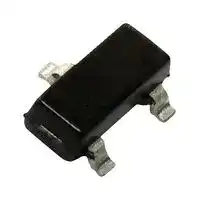
- Diode Mounting: Surface Mount
- Diode Case Style: SOT-23
- Diode Configuration: Dual Common Cathode
- Forward Voltage Max: 1.25V
- Forward Surge Current: 2A
- Reverse Recovery Time: 50ns
- Average Forward Current: 200mA
- Operating Temperature Max: 150°C
- Repetitive Peak Reverse Voltage: 250V
| Delivery and price | |
|---|---|
| Units per pack | 3000 |
| Price | 0.068 € |
| Current stock | 10+ |
| Lead time | 30 days |
## **Is Now Part of**

## **To learn more about ON Semiconductor, please visit our website at www.onsemi.com**

Please note: As part of the Fairchild Semiconductor integration, some of the Fairchild orderable part numbers will need to change in order to meet ON Semiconductor’s system requirements. Since the ON Semiconductor product management systems do not have the ability to manage part nomenclature that utilizes an underscore (_), the underscore (_) in the Fairchild part numbers will be changed to a dash (-). This document may contain device numbers with an underscore (_). Please check the ON Semiconductor website to verify the updated device numbers. The most current and up-to-date ordering information can be found at www.onsemi.com. Please email any questions regarding the system integration to Fairchild_questions@onsemi.com.

ON Semiconductor and the ON Semiconductor logo are trademarks of Semiconductor Components Industries, LLC dba ON Semiconductor or its subsidiaries in the United States and/or other countries. ON Semiconductor owns the rights to a number of patents, trademarks, copyrights, trade secrets, and other intellectual property. A listing of ON Semiconductor’s product/patent coverage may be accessed at www.onsemi.com/site/pdf/Patent-Marking.pdf. ON Semiconductor reserves the right to make changes without further notice to any products herein. ON Semiconductor makes no warranty, representation or guarantee regarding the suitability of its products for any particular purpose, nor does ON Semiconductor assume any liability arising out of the application or use of any product or circuit, and specifically disclaims any and all liability, including without limitation special, consequential or incidental damages. Buyer is responsible for its products and applications using ON Semiconductor products, including compliance with all laws, regulations and safety requirements or standards, regardless of any support or applications information provided by ON Semiconductor. “Typical” parameters which may be provided in ON Semiconductor data sheets and/or specifications can and do vary in different applications and actual performance may vary over time. All operating parameters, including “Typicals” must be validated for each customer application by customer’s technical experts. ON Semiconductor does not convey any license under its patent rights nor the rights of others. ON Semiconductor products are not designed, intended, or authorized for use as a critical component in life support systems or any FDA Class 3 medical devices or medical devices with a same or similar classification in a foreign jurisdiction or any devices intended for implantation in the human body. Should Buyer purchase or use ON Semiconductor products for any such unintended or unauthorized application, Buyer shall indemnify and hold ON Semiconductor and its officers, employees, subsidiaries, affiliates, and distributors harmless against all claims, costs, damages, and expenses, and reasonable attorney fees arising out of, directly or indirectly, any claim of personal injury or death associated with such unintended or unauthorized use, even if such claim alleges that ON Semiconductor was negligent regarding the design or manufacture of the part. ON Semiconductor is an Equal Opportunity/Affirmative Action Employer. This literature is subject to all applicable copyright laws and is not for resale in any manner.

**==> picture [64 x 7] intentionally omitted <==**

**----- Start of picture text -----**<br>
November 2014<br>**----- End of picture text -----**<br>


**MMBD1401A / MMBD1403A / MMBD1404A / MMBD1405A High-Voltage General-Purpose Diode**

## **Descriptions**

Sourced from process 2V.

## **Connection Diagram**

**==> picture [60 x 72] intentionally omitted <==**

**----- Start of picture text -----**<br>
3<br>2<br>¢<br>1<br>SOT-23<br>**----- End of picture text -----**<br>


**==> picture [117 x 112] intentionally omitted <==**

**----- Start of picture text -----**<br>
1401A 1403A<br>3 3<br>1 2NC 1 2<br>1404A 1405A<br>3 3<br>1 2 1 2<br>**----- End of picture text -----**<br>


## **Ordering Information**

|**Part Number**|**Top Mark**|**Package**|**Packing Method**|
|---|---|---|---|
|MMBD1401A|A29|SOT-23 3L|Tape and Reel|
|MMBD1403A|A32|SOT-23 3L|Tape and Reel|
|MMBD1404A|A33|SOT-23 3L|Tape and Reel|
|MMBD1405A|A34|SOT-23 3L|Tape and Reel|


© 2004 Fairchild Semiconductor Corporation MMBD1401A / MMBD1403A / MMBD1404A / MMBD1405A Rev. 1.1.0

www.fairchildsemi.com

## **Absolute Maximum Ratings**[(1), (2)]

Stresses exceeding the absolute maximum ratings may damage the device. The device may not function or be operable above the recommended operating conditions and stressing the parts to these levels is not recommended. In addition, extended exposure to stresses above the recommended operating conditions may affect device reliability. The absolute maximum ratings are stress ratings only. Values are at TA = 25°C unless otherwise noted.

|**Symbol**|**Parameter**|**Parameter**|**Value**|**Unit**|
|---|---|---|---|---|
|WIV|Working Inverse Voltage||175|V|
|IO|Average Rectified Current||200|mA|
|IF|DC Forward Current||600|mA|
|if|Recurrent Peak Forward Current||700|mA|
|if(surge)|Non-Repetitive Peak Forward<br>Surge Current|Pulse Width = 1.0 second|1.0|A|
|||Pulse Width = 1.0 microsecond|2.0||
|TSTG|Storage Temperature Range||-55 to +150|°C|
|TJ|Operating Junction Temperature||150|°C|


## **Notes:**

1. These ratings are based on a maximum junction temperature of 150 ° C.

2. These are steady-state limits. Fairchild Semiconductor should be consulted on applications involving pulsed or low-duty-cycle operations.

## **Thermal Characteristics**[(3)]

Values are at TA = 25°C unless otherwise noted.

|**Symbol**|**Parameter**|**Max.**|**Unit**|
|---|---|---|---|
|PD|Power Dissipation|350|mW|
||Derate above 25°C|2.8|mW/°C|
|RθJA|Thermal Resistance, Junction-to-Ambient|357|°C/W|


## **Note:**

3. Device is mounted on glass epoxy PCB 1.6 inch × 1.6 inch × 0.06 inch, mounting pad for the collector lead minimum

- 0.93 in[2] .

## **Electrical Characteristics**

Values are at TA = 25°C unless otherwise noted.

|**Symbol**|**Parameter**|**Conditions**|**Min.**|**Max.**|**Unit**|
|---|---|---|---|---|---|
|BV|Breakdown Voltage|IR= 100μA|250||V|
|IR|Reverse Current|VR= 120 V||40|nA|
|||VR= 175 V||100|nA|
|VF|Forward Voltage|IF= 10 mA||800|mV|
|||IF= 50 mA|760|920|mV|
|||IF= 200 mA||1.1|V|
|||IF= 300 mA||1.25|V|
|CO|Diode Capacitance|VR= 0, f = 1.0 MHz||2.0|pF|
|TRR|Reverse Recovery Time|IF= IR= 30 mA,<br>IRR= 1.0 mA, RL= 100Ω||50|nS|


© 2004 Fairchild Semiconductor Corporation MMBD1401A / MMBD1403A / MMBD1404A / MMBD1405A Rev. 1.1.0

www.fairchildsemi.com

2

## **Typical Performance Characteristics**

**==> picture [428 x 309] intentionally omitted <==**

**----- Start of picture text -----**<br>
325 Ta= 25°C 50 a Ta= 25°C<br>Pett 40 a ee<br>Pe ee ee<br>30<br>Pee eee _——- a<br>300<br>ne 20 a<br>Oe SS Eee<br>Lf tier ET EE 10 a a<br>275 eeee ee 055 75 95 115 135 155 175 195<br>3 5 10 20 30 50 100 V    - REVERSE VOLTAGE (V)R<br>I   - REVERSE CURRENT  (uA)R GENERAL RULE: The Reverse Current of a diode will approximately<br>double for every ten (10) Degree C increase in Temperature<br>Figure 1. Reverse Voltage vs. Reverse Current Figure 2. Reverse Current vs. Reverse Voltage<br>BV - 1.0 to 100  μ A IR - 55 to 205 V<br>100 Ta= 25°C<br>Ta= 25°C a 450 ee ee<br>90<br>S———— Pe ear<br>80<br>400<br>70 ee ET TT<br>60 a—— ea e eeeeeee ae<br>350<br>50<br>_ | : eeeee7 eel<br>40<br>ee a 300 a<br>30 a  eea pa<br>20 I a Ee ZO<br>180 200 220 240 255 250 La] fet tT<br>V    - REVERSE VOLTAGE (V)R ct |tttET<br>GENERAL RULE: The Reverse Current of a diode will approximately 1 2 3 5 10 20 30 50 100<br>double for every ten Degree C increase in Temperature I   - FORWARD CURRENT  (uA)F<br>R<br>R<br>R<br>F<br>R<br>VV    - REVERSE VOLTAGE (V) I    - REVERSE CURRENT (nA)<br>II    - REVERSE CURRENT (nA)R F<br>VV    - FORWARD VOLTAGE (mV)<br>**----- End of picture text -----**<br>


**Figure 3. Reverse Current vs. Reverse Voltage IR - 180 to 255 V**

**Figure 4. Forward Voltage vs. Forward Current VF - 1.0 to 100** μ **A**

**==> picture [431 x 137] intentionally omitted <==**

**----- Start of picture text -----**<br>
VF - 0.1 to 10 mA<br>700725 Ta= 25°C 1.4 Ta= 25 ° C<br>— ee 1.3 Ea<br>a pe<br>650600 PoCT eT 1.21.1 poI} +H +at<br>re eee rea<br>De 1 ee<br>550<br>a ee 0.9 ee ae<br>ee a re<br>500 Lo]a es| Titeeof eeTy 0.8 eerr =2<br>4500.1 Rr 0.2 0.3 0.5 1 ST 2 3 5 10 0.710 ee 20 30 50 100 ee 200 300 500 800<br>I   - FORWARD CURRENT  (mA)F I   - FORWARD CURRENT  (mA)F<br>VV    - FORWARD VOLTAGE (mV)FF VV    - FORWARD VOLTAGE (mV)FF<br>**----- End of picture text -----**<br>


**==> picture [195 x 19] intentionally omitted <==**

**----- Start of picture text -----**<br>
Figure 5. Forward Voltage vs. Forward Current<br>VF - 0.1 to 10 mA<br>**----- End of picture text -----**<br>


**==> picture [195 x 19] intentionally omitted <==**

**----- Start of picture text -----**<br>
Figure 6. Forward Voltage vs. Forward Current<br>VF - 10 to 800 mA<br>**----- End of picture text -----**<br>


© 2004 Fairchild Semiconductor Corporation MMBD1401A / MMBD1403A / MMBD1404A / MMBD1405A Rev. 1.1.0

www.fairchildsemi.com

3

## **Typical Performance Characteristics** (Continued)

**==> picture [439 x 511] intentionally omitted <==**

**----- Start of picture text -----**<br>
1.3<br>Ta= 25°C<br>800 LL EUAN LTE ETE TT Po<br>a Ta= -40°C 1.2 TT tT<br>600 cae Ta= 25°C lll 1.1 PHi ttt ty Pt et<br>a REECE EEE EEEEEE<br>1<br>400 ern aecee en Tmalll P SECPSSEEEE E<br>Ta= +80°C<br>0.9<br>200 cea HEEEPERRSSSS<br>eT OI CCI CT 0.8 SeeEC<br>0.001 0.003 0.01 0.03 0.1 0.3 1 3 10 0 2 4 6 8 10 12 14 15<br>I   - FORWARD CURRENT  (mA)F REVERSE VOLTAGE (V)<br>Figure 7. Forward Voltage vs. Ambient Temperature Figure 8. Capacitance vs. Reverse Voltage<br>VF -  1.0  μ A - 10 mA (- 40 to +80 ° C)<br>50 PEELESPELTEE 500400 Hs}ee_}+_+_+_| +<br>40 aa 300 a<br>PPR EEE a<br>200<br>30 PELLET PR RAT LL ———<br>PEELE EEE ce 100 a<br>  IF = IR = 30 mA<br>PEELE Rloop = 100 Ohms a<br>20 TEE E TEE 0 [EES<br>1 1.5 2 2.5 3 0 50 100 150<br>Irr - REVERSE RECOVERY CURRENT (mA) T  - AMBIENT TEMPERATURE  (   C) A o<br>Figure 9. Reverse Recovery Time vs. Figure 10. Average Rectified Current(IO) andO) and) and<br>Reverse Recovery Current (Irr) Forward Current (IF) vs. Ambient Temperature(TAF) vs. Ambient Temperature(TA) vs. Ambient Temperature(TAA)<br>500 EN<br>400 | |N | ee| | eeef |<br>DO-35 Pkg<br>300 Reenn<br>200 FN SOT-23 Pkg Nf<br>100 SAR SES<br>| | | | |N KE<br>0 | | | | |INN1<br>0 50 100 150 200<br>I   - AVERAGE TEMPERATURE  (  C)O o<br>Io - AVERAGE RECTIFIED CURRENT - mA<br>I    - FORWARD CURRENT STEADY STATE - mAR<br>D<br>F<br>CAPACITANCE (pF)<br>F<br>VV    - FORWARD VOLTAGE (mV)<br>I - CURRENT (mA)<br>REVERSE RECOVERY (nS)<br>P   - POWER DISSIPATION (mW)<br>**----- End of picture text -----**<br>


**Figure 10. Average Rectified Current(IO) andO) and) and Forward Current (IF) vs. Ambient Temperature(TAF) vs. Ambient Temperature(TA) vs. Ambient Temperature(TAA)**

**Figure 11. Power Derating Curve**

© 2004 Fairchild Semiconductor Corporation MMBD1401A / MMBD1403A / MMBD1404A / MMBD1405A Rev. 1.1.0

www.fairchildsemi.com

4

**==> picture [127 x 58] intentionally omitted <==**

**==> picture [52 x 44] intentionally omitted <==**

**==> picture [45 x 62] intentionally omitted <==**

**==> picture [155 x 95] intentionally omitted <==**

**==> picture [45 x 62] intentionally omitted <==**

**==> picture [81 x 44] intentionally omitted <==**

ON Semiconductor and      are trademarks of Semiconductor Components Industries, LLC dba ON Semiconductor or its subsidiaries in the United States and/or other countries. ON Semiconductor owns the rights to a number of patents, trademarks, copyrights, trade secrets, and other intellectual property. A listing of ON Semiconductor’s product/patent coverage may be accessed at www.onsemi.com/site/pdf/Patent−Marking.pdf. ON Semiconductor reserves the right to make changes without further notice to any products herein. ON Semiconductor makes no warranty, representation or guarantee regarding the suitability of its products for any particular purpose, nor does ON Semiconductor assume any liability arising out of the application or use of any product or circuit, and specifically disclaims any and all liability, including without limitation special, consequential or incidental damages. Buyer is responsible for its products and applications using ON Semiconductor products, including compliance with all laws, regulations and safety requirements or standards, regardless of any support or applications information provided by ON Semiconductor. “Typical” parameters which may be provided in ON Semiconductor data sheets and/or specifications can and do vary in different applications and actual performance may vary over time. All operating parameters, including “Typicals” must be validated for each customer application by customer’s technical experts. ON Semiconductor does not convey any license under its patent rights nor the rights of others. ON Semiconductor products are not designed, intended, or authorized for use as a critical component in life support systems or any FDA Class 3 medical devices or medical devices with a same or similar classification in a foreign jurisdiction or any devices intended for implantation in the human body. Should Buyer purchase or use ON Semiconductor products for any such unintended or unauthorized application, Buyer shall indemnify and hold ON Semiconductor and its officers, employees, subsidiaries, affiliates, and distributors harmless against all claims, costs, damages, and expenses, and reasonable attorney fees arising out of, directly or indirectly, any claim of personal injury or death associated with such unintended or unauthorized use, even if such claim alleges that ON Semiconductor was negligent regarding the design or manufacture of the part. ON Semiconductor is an Equal Opportunity/Affirmative Action Employer. This literature is subject to all applicable copyright laws and is not for resale in any manner.

## **PUBLICATION ORDERING INFORMATION**

**N. American Technical Support** : 800−282−9855 Toll Free **ON Semiconductor Website** : **www.onsemi.com** USA/Canada

## **LITERATURE FULFILLMENT** :

Literature Distribution Center for ON Semiconductor

**Order Literature** : http://www.onsemi.com/orderlit For additional information, please contact your local Sales Representative

19521 E. 32nd Pkwy, Aurora, Colorado 80011 USA **Europe, Middle East and Africa Technical Support: Phone** : 303−675−2175 or 800−344−3860 Toll Free USA/Canada Phone: 421 33 790 2910 **Fax** : 303−675−2176 or 800−344−3867 Toll Free USA/Canada **Japan Customer Focus Center Email** : orderlit@onsemi.com Phone: 81−3−5817−1050

© Semiconductor Components Industries, LLC

www.onsemi.com

**www.onsemi.com**

**1**
Updated at June 8, 2026
onsemi is a premier global supplier of intelligent power and sensing technologies, driving disruptive innovations across the automotive, industrial, and cloud infrastructure markets. Recognized for their commitment to sustainability and reliable supply chains, the company accelerates advancements in vehicle electrification, industrial automation, and 5G networks by solving the industry's most complex design challenges. At the core of their portfolio is an industry-leading selection of discrete semiconductors. This extensive range features thousands of high-performance bipolar transistors, single and dual MOSFETs, and a comprehensive array of diodes, including Zener, Schottky, and fast-recovery rectifiers. Engineered for superior thermal performance and energy efficiency, these foundational components are critical for demanding power conversion, switching, and signal conditioning applications. Beyond essential discretes, onsemi provides a robust suite of advanced power management and circuit protection solutions. Their lineup includes intelligent power modules, single IGBTs, and transient voltage suppression (TVS) diodes designed to safeguard sensitive circuitry. Complimented by integrated passive filters, AC/DC LED driver ICs, and specialized sub-2.4GHz RF transceivers, onsemi equips engineers with the scalable, high-quality technologies needed to build a cleaner, smarter, and more connected world.
About Novapart
Novapart is a B2B electronic component broker specialising in stock shortages and cost reduction. We source hard-to-find parts and identify compliant alternatives across a catalogue of 410,000+ components from 500+ manufacturers.
Learn more →Stock Shortage Specialist
When a component is unavailable, discontinued or has an unacceptable lead time, we tap into our network of vetted European and Asian distributors to source what you need — without compromising on quality or traceability.
Request a quote →Compliant Alternatives
We identify pin-to-pin, electrically equivalent substitutes that meet the same certifications (RoHS, AEC-Q100, REACH) as your original specification — validated against datasheets, not just part numbers. Often at a lower cost.
BOM Analysis service →