
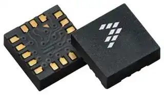


MMA9553LR1
MEMS Accelerometer, Motion-Sensing, Digital, X, Y, Z, ± 2g, ± 4g, ± 8g, 1.71 V, 1.89 V, LGA
- Manufacturer: NXP
- Product type: MEMS Accelerometers
- No. of Pins: 16Pins
- Sensitivity Max: 0.244mg/LSB
- Sensitivity Min: 0.061mg/LSB
- Sensitivity Typ: 0.061mg/LSB, 0.122mg/LSB, 0.244mg/LSB
- Measurement Axis: X, Y, Z
- Sensor Case Style: LGA
- Acceleration Range: ± 2g, ± 4g, ± 8g
- MEMS Sensor Output: Digital
- Supply Voltage Max: 1.89V
- Supply Voltage Min: 1.71V
| Delivery and price | |
|---|---|
| Units per pack | 100 |
| Price | 2.17 € |
| Current stock | 10+ |
| Lead time | 30 days |
**Freescale Semiconductor** Data Sheet: Technical Data

Document Number: MMA955xL Rev. 3.1, 5/2015

An Energy Efficient Solution by Freescale

## **MMA955xL Intelligent Motion-Sensing Platform**

The MMA955xL device an intelligent sensor, incorporating dedicated accelerometer MEMS transducers, signal conditioning, data conversion, and a 32-bit programmable microcontroller.

This unique blend transforms Freescale’s MMA955xL into an intelligent, highprecision, motion-sensing platform able to manage multiple sensor inputs. This device can make system-level decisions required for sophisticated applications such as gesture recognition, pedometer functionality, tilt compensation and calibration, and activity monitoring.

## **MMA9550L MMA9551L MMA9553L MMA9559L**

**==> picture [90 x 10] intentionally omitted <==**

**----- Start of picture text -----**<br>
Top and bottom view<br>**----- End of picture text -----**<br>


The MMA955xL device is programmed and configured with the CodeWarrior Development Studio for Microcontrollers software, version 10.1 or later. This standard integrated design environment enables customers to quickly implement custom algorithms and features to exactly match their application needs.

Using the master I[2] C port, the MMA955xL device can manage secondary sensors, such as pressure sensors, magnetometers, or gyroscopes. This allows sensor initialization, calibration, data compensation, and computation functions to be off-loaded from the system application processor. The MMA955xL device also acts as an intelligent sensing hub and a highly configurable decision engine. Total system power consumption is significantly reduced because the application processor stays powered down until absolutely needed.

## **Hardware Features**

- Three accelerometer operating ranges:

   - ±2 _g_ suits most hand gestures (orientation detection and tilt control) and freefall. For tap detection, ±4 _g_ and ±8 _g_ are supported.

   - ±4 _g_ covers most regular human dynamics (walking and jogging)

   - ±8 _g_ detects most abrupt activities (gaming)

- Integrated temperature sensor

- One slave SPI or I[2] C interface operating at up to 2 Mbps, dedicated to communication with the host processor. Default value of the I[2] C, 7-bit address is 0x4C. (This can be customized by firmware.)

- One master I[2] C interface operating at up to 400 kbps that can be used to communicate with external sensors

- Eight selectable output data rates (ODR), from 488 Hz to 3.8 Hz (extending farther from 3906 Hz to 0.24 Hz with MMA9559L Firmware version)

- 10, 12, 14, and 16-bit trimmed ADC data formats available

- 1.8 V supply voltage

- 32-bit CPU with MAC unit

- Extensive set of power-management features and low-power modes

**==> picture [82 x 27] intentionally omitted <==**

**----- Start of picture text -----**<br>
16-pin LGA<br>3 mm x 3 mm x 1 mm<br>Case 2094-01<br>**----- End of picture text -----**<br>


**==> picture [177 x 221] intentionally omitted <==**

**----- Start of picture text -----**<br>
Top view<br>VDD 1 _ uuu 16 15 14 C 13 RGPIO7/AN1/TPMCH1<br>BKGD-MS/RGPIO9 2 7C 12 RGPIO6/AN0TPMCH0<br>RESETB 3 Jc 11 RGPIO5/PDB_A/<br>INT_O<br>SCL0/RGPIO0 4<br>SCLK Jc 10 VSS<br>VSS 5 Jooo 6 7 8 C 9 RGPIO4/INT<br>Pin connections<br>SSA DDA<br>V RGPIO8/PDB_B V<br>SDA0/RGPIO1/SDI RGPIO2/SCL1/SDO RGPIO3/SDA1/SSB<br>**----- End of picture text -----**<br>


- Integrated 16-bit resolution ADC can be used to convert external analog signals

- Single-Wire, Background-Debug Mode (BDM) pin interface

- 16-KB flash memory

- 2-KB Random Access Memory

- ROM-based flash controller and slave-port, command-line interpreter

- Two-channel timer with input capture, output capture, or edge-aligned PWM

- Programmable delay block for scheduling events relative to start of frame

- A 16-bit, modulo timer for scheduling periodic events

- Minimal external component requirements

- RoHS compliant (–40ºC to +85ºC), 16-pin, 3 x 3 x 1-mm LGA package

© 2011, 2013, 2015 Freescale Semiconductor, Inc. All rights reserved.

## **Software Features**

This device can be programmed to provide any of the following:

- Orientation detection (portrait/landscape)

- High- _g_ /Low- _g_ threshold detection

- Pulse detection (single, double and directional tap)

- Tilt detection

- Auto wake/sleep

- Embedded, smart FIFO

- Power management

- Pedometer

A selection of the software features are included in the factory-programmed firmware for some devices. Users may add their own features with user firmware.The power and flexibility of the embedded ColdFire V1 MCU core associated with the high performance 3-axis accelerometer give new and unprecedented capabilities to the MMA955xL devices family.

**Table 1. Ordering information**

|**Part number**|**Firmware**|**Temperature range**|**Package description**|**Shipping**|
|---|---|---|---|---|
|MMA9550LR1|Motion|–40°C to +85°C|LGA-16|Tape and reel|
|MMA9551LR1|Gesture|–40°C to +85°C|LGA-16|Tape and reel|
|MMA9553LR1|Pedometer|–40°C to +85°C|LGA-16|Tape and reel|
|MMA9559LR1|Foundation|–40°C to +85°C|LGA-16|Tape and reel|


**MMA955xL**

Sensors Freescale Semiconductor, Inc.

2

## **Contents**

|**1**|**Variations of MMA955xL Device . . . . . . . . . . . . . . . . . . . . . . . . . . . . . . . . . . . . . . . . . . . . . . . . . . . . . . . . . . . . . . . . . . . .  4**|
|---|---|
|**2**|**Typical Applications. . . . . . . . . . . . . . . . . . . . . . . . . . . . . . . . . . . . . . . . . . . . . . . . . . . . . . . . . . . . . . . . . . . . . . . . . . . . . .  6**|
|**3**|**General Description . . . . . . . . . . . . . . . . . . . . . . . . . . . . . . . . . . . . . . . . . . . . . . . . . . . . . . . . . . . . . . . . . . . . . . . . . . . . . .  7**|
||3.1. . Functional Overview . . . . . . . . . . . . . . . . . . . . . . . . . . . . . . . . . . . . . . . . . . . . . . . . . . . . . . . . . . . . . . . . . . . . . . . . . .  7|
||3.2. . Packaging Information . . . . . . . . . . . . . . . . . . . . . . . . . . . . . . . . . . . . . . . . . . . . . . . . . . . . . . . . . . . . . . . . . . . . . . . .  8|
||3.2.1<br>Package diagrams. . . . . . . . . . . . . . . . . . . . . . . . . . . . . . . . . . . . . . . . . . . . . . . . . . . . . . . . . . . . . . . . . . . . . .  8|
||3.2.2<br>Sensing Direction and Output Response  . . . . . . . . . . . . . . . . . . . . . . . . . . . . . . . . . . . . . . . . . . . . . . . . . . . .  9|
||3.2.3<br>Pin Functions. . . . . . . . . . . . . . . . . . . . . . . . . . . . . . . . . . . . . . . . . . . . . . . . . . . . . . . . . . . . . . . . . . . . . . . . . .  9|
||3.3. . Pin Function Descriptions. . . . . . . . . . . . . . . . . . . . . . . . . . . . . . . . . . . . . . . . . . . . . . . . . . . . . . . . . . . . . . . . . . . . .  10|
||3.4. . System Connections. . . . . . . . . . . . . . . . . . . . . . . . . . . . . . . . . . . . . . . . . . . . . . . . . . . . . . . . . . . . . . . . . . . . . . . . .  10|
||3.4.1<br>Power Sequencing  . . . . . . . . . . . . . . . . . . . . . . . . . . . . . . . . . . . . . . . . . . . . . . . . . . . . . . . . . . . . . . . . . . . .  10|
||3.4.2<br>Layout Recommendations. . . . . . . . . . . . . . . . . . . . . . . . . . . . . . . . . . . . . . . . . . . . . . . . . . . . . . . . . . . . . . .  10|
||3.4.3<br>MMA955xL Platform as an Intelligent Slave . . . . . . . . . . . . . . . . . . . . . . . . . . . . . . . . . . . . . . . . . . . . . . . . .  11|
||3.4.4<br>MMA955xL Platform as a Sensor Hub  . . . . . . . . . . . . . . . . . . . . . . . . . . . . . . . . . . . . . . . . . . . . . . . . . . . . .  13|
|**4**|**Mechanical and Electrical Specifications. . . . . . . . . . . . . . . . . . . . . . . . . . . . . . . . . . . . . . . . . . . . . . . . . . . . . . . . . . . .  14**|
||4.1. . Definitions. . . . . . . . . . . . . . . . . . . . . . . . . . . . . . . . . . . . . . . . . . . . . . . . . . . . . . . . . . . . . . . . . . . . . . . . . . . . . . . . .  14|
||4.2. . Pin Groups . . . . . . . . . . . . . . . . . . . . . . . . . . . . . . . . . . . . . . . . . . . . . . . . . . . . . . . . . . . . . . . . . . . . . . . . . . . . . . . .  14|
||4.3. . Absolute Maximum Ratings . . . . . . . . . . . . . . . . . . . . . . . . . . . . . . . . . . . . . . . . . . . . . . . . . . . . . . . . . . . . . . . . . . .  14|
||4.4. . Operating Conditions . . . . . . . . . . . . . . . . . . . . . . . . . . . . . . . . . . . . . . . . . . . . . . . . . . . . . . . . . . . . . . . . . . . . . . . .  15|
||4.5. . Electrostatic Discharge (ESD) and Latch-up Protection Characteristics  . . . . . . . . . . . . . . . . . . . . . . . . . . . . . . . . .  15|
||4.6. . General DC Characteristics . . . . . . . . . . . . . . . . . . . . . . . . . . . . . . . . . . . . . . . . . . . . . . . . . . . . . . . . . . . . . . . . . . .  15|
||4.7. . Supply Current Characteristics. . . . . . . . . . . . . . . . . . . . . . . . . . . . . . . . . . . . . . . . . . . . . . . . . . . . . . . . . . . . . . . . .  16|
||4.8. . Accelerometer Transducer Mechanical Characteristics . . . . . . . . . . . . . . . . . . . . . . . . . . . . . . . . . . . . . . . . . . . . . .  16|
||4.9. . ADC Characteristics . . . . . . . . . . . . . . . . . . . . . . . . . . . . . . . . . . . . . . . . . . . . . . . . . . . . . . . . . . . . . . . . . . . . . . . . .  16|
||4.10. ADC Sample Rates  . . . . . . . . . . . . . . . . . . . . . . . . . . . . . . . . . . . . . . . . . . . . . . . . . . . . . . . . . . . . . . . . . . . . . . . . .  17|
||4.11. AC Electrical Characteristics  . . . . . . . . . . . . . . . . . . . . . . . . . . . . . . . . . . . . . . . . . . . . . . . . . . . . . . . . . . . . . . . . . .  18|
||4.12. General Timing Control  . . . . . . . . . . . . . . . . . . . . . . . . . . . . . . . . . . . . . . . . . . . . . . . . . . . . . . . . . . . . . . . . . . . . . .  18|
||4.13. I2C Timing. . . . . . . . . . . . . . . . . . . . . . . . . . . . . . . . . . . . . . . . . . . . . . . . . . . . . . . . . . . . . . . . . . . . . . . . . . . . . . . . .  19|
||4.13.1 Slave I2C . . . . . . . . . . . . . . . . . . . . . . . . . . . . . . . . . . . . . . . . . . . . . . . . . . . . . . . . . . . . . . . . . . . . . . . . . . . .  19|
||4.13.2 Master I2C Timing . . . . . . . . . . . . . . . . . . . . . . . . . . . . . . . . . . . . . . . . . . . . . . . . . . . . . . . . . . . . . . . . . . . . .  19|
||4.14. Slave SPI Timing  . . . . . . . . . . . . . . . . . . . . . . . . . . . . . . . . . . . . . . . . . . . . . . . . . . . . . . . . . . . . . . . . . . . . . . . . . . .  20|
||4.15. Flash Parameters . . . . . . . . . . . . . . . . . . . . . . . . . . . . . . . . . . . . . . . . . . . . . . . . . . . . . . . . . . . . . . . . . . . . . . . . . . .  21|
|**5**|**Package Information  . . . . . . . . . . . . . . . . . . . . . . . . . . . . . . . . . . . . . . . . . . . . . . . . . . . . . . . . . . . . . . . . . . . . . . . . . . . .  22**|
||5.1. . Footprint and pattern information . . . . . . . . . . . . . . . . . . . . . . . . . . . . . . . . . . . . . . . . . . . . . . . . . . . . . . . . . . . . . . .  22|
||5.2. . Marking. . . . . . . . . . . . . . . . . . . . . . . . . . . . . . . . . . . . . . . . . . . . . . . . . . . . . . . . . . . . . . . . . . . . . . . . . . . . . . . . . . .  23|
||5.3. . Tape and reel information. . . . . . . . . . . . . . . . . . . . . . . . . . . . . . . . . . . . . . . . . . . . . . . . . . . . . . . . . . . . . . . . . . . . .  24|
|**6**|**Revision History . . . . . . . . . . . . . . . . . . . . . . . . . . . . . . . . . . . . . . . . . . . . . . . . . . . . . . . . . . . . . . . . . . . . . . . . . . . . . . . .  25**|


## **Related Documentation**

The MMA955xL device features and operations are described in a variety of reference manuals, user guides, and application notes. To find the most-current versions of these documents:

1. Go to the Freescale homepage at freescale.com.

2. In the Keyword search box at the top of the page, enter the device number MMA955xL.

3. In the Refine Your Result pane on the left, click on the Documentation link.

**MMA955xL**

Sensors Freescale Semiconductor, Inc.

3

**1 Variations of MMA955xL Device**

Freescale offers a variety of firmware versions for the MMA955xL devices. The different versions of the device are identified by the fourth digit in the part number (for example MMA955 **9L** ). Information and specifications provided in this data sheet are independent of the Freescale firmware versions.

The following table lists some of the variations among the MMA955xL-platform devices.

**Table 2. Features of product-line devices**

|**Feature - Device**<br>~~ee~~|**MMA9550L**<br>~~ee~~|**MMA9551L**<br>~~ee~~|**MMA9553L**<br>~~ee~~|**MMA9559L**<br>~~ee~~|
|---|---|---|---|---|
|Key elements<br>~~ee~~<br>~~GG~~|Motion sensing<br>~~ee~~<br>~~GG~~|Gesture sensing<br>~~ee~~<br>~~GG~~|Pedometer<br>~~ee~~<br>~~GG~~|High flexibility<br>~~ee~~<br>~~GG~~|
|User flash available<br>~~GG~~<br>~~Ge~~|6.5 KB<br>~~GG~~<br>~~Ge~~|4.5 KB<br>~~GG~~<br>~~Ge~~|1.0 KB<br>~~GG~~<br>~~Ge~~|14 KB<br>~~GG~~<br>~~Ge~~|
|User RAM available<br>~~GG~~|576 bytes<br>~~GG~~|452 bytes<br>~~GG~~|420 bytes<br>~~GG~~|1664 bytes<br>~~GG~~|
|ADC resolution (bits)<br>~~Ge~~|10,12,14,16 bits<br>~~Ge~~|10,12,14,16 bits<br>~~Ge~~|10,12,14,16 bits<br>~~Ge~~|10,12,14,16 bits<br>~~Ge~~|
|_g_measurement ranges<br>~~GD~~|2_g_, 4_g_, 8_g_<br>~~GD~~|2_g_, 4_g_, 8_g_<br>~~GD~~|2_g_, 4_g_, 8_g_<br>~~GD~~|2_g_, 4_g_, 8_g_<br>~~GD~~|
|Real-time and preemptive scheduling<br>~~GO~~|Yes<br>~~GO~~|Yes<br>~~GO~~|Yes<br>~~GO~~|No<br>~~GO~~|
|Event management<br>~~GO~~<br>~~Ge~~|No<br>~~GO~~<br>~~Ge~~|No<br>~~GO~~<br>~~Ge~~|No<br>~~GO~~<br>~~Ge~~|Yes<br>~~GO~~<br>~~Ge~~|
|Slave Port Command Interpreter<br>~~Ge~~<br>~~Ge~~|~~Ge~~<br>~~Ge~~||||
|• Normal mode<br>~~Ge~~<br>~~ee~~|Yes<br>~~Ge~~<br>~~ee~~|Yes<br>~~Ge~~<br>~~ee~~|Yes<br>~~Ge~~<br>~~ee~~|No<br>~~Ge~~<br>~~ee~~|
|• Legacy mode<br>~~Ge~~|Yes<br>~~Ge~~|Yes<br>~~Ge~~|Yes<br>~~Ge~~|No<br>~~Ge~~|
|• Streaming mode<br>~~Ge~~<br>~~ss~~|Yes<br>~~Ge~~<br>~~ss~~|Yes<br>~~Ge~~<br>~~ss~~|Yes<br>~~Ge~~<br>~~ss~~|No<br>~~Ge~~<br>~~ss~~|
|Front-end processing<br>~~ss~~<br>~~a ~~|~~ss~~<br> ~~G~~||||
|• 100-Hz BW anti-aliasing<br>~~Ge~~|Yes<br>~~Ge~~<br>~~es~~|Yes<br>~~Ge~~|Yes<br>~~Ge~~|No<br>~~Ge~~|
|• 50-Hz BW anti-aliasing<br>~~es~~|Yes<br>~~es~~<br>~~es~~|Yes<br>~~es~~|Yes<br>~~es~~|No<br>~~es~~|
|• _g_-mode-dependent resolution<br>~~es~~<br>~~se~~|Yes<br>~~es~~<br>~~es~~<br>~~se~~|Yes<br>~~es~~<br>~~se~~|Yes<br>~~es~~<br>~~se~~|Yes<br>~~es~~<br>~~se~~|
|• Absolute value<br>~~Ge~~|Yes<br>~~Ge~~<br>~~es~~|Yes<br>~~Ge~~|Yes<br>~~Ge~~|No<br>~~Ge~~|
|• Low-pass filter<br>~~es~~|Yes<br>~~es~~<br>~~es~~|Yes<br>~~es~~|Yes<br>~~es~~|No<br>~~es~~|
|• High-pass filter<br>~~es~~<br>~~se~~|Yes<br>~~es~~<br>~~es~~<br>~~se~~|Yes<br>~~es~~<br>~~se~~|Yes<br>~~es~~<br>~~se~~|No<br>~~es~~<br>~~se~~|
|• Data-ready interrupt<br>~~Ge~~|Yes<br>~~Ge~~|Yes<br>~~Ge~~|Yes<br>~~Ge~~|Yes<br>~~Ge~~|
|Gesture applications<br>~~Ge~~|~~Ge~~||||
|• High_g_/Low_g_<br>~~Ge~~<br>~~es~~|No<br>~~Ge~~<br>~~es~~|Yes<br>~~Ge~~<br>~~es~~|No<br>~~Ge~~<br>~~es~~|No<br>~~Ge~~<br>~~es~~|
|• Tilt<br>~~ss~~|No<br>~~ss~~|Yes<br>~~ss~~|No<br>~~ss~~|No<br>~~ss~~|
|• Portrait/Landscape<br>~~Ge~~|No<br>~~Ge~~|Yes<br>~~Ge~~|No<br>~~Ge~~|No<br>~~Ge~~|
|• Programmable orientation<br>~~Ge~~<br>~~ss~~|No<br>~~Ge~~<br>~~ss~~|Yes<br>~~Ge~~<br>~~ss~~|No<br>~~Ge~~<br>~~ss~~|No<br>~~Ge~~<br>~~ss~~|
|• Tap/Double-tap<br>~~se~~|No<br>~~se~~<br>~~es~~|Yes<br>~~se~~|No<br>~~se~~|No<br>~~se~~|
|• Freefall<br>~~es~~|No<br>~~es~~<br>~~es~~|Yes<br>~~es~~|No<br>~~es~~|No<br>~~es~~|
|• Motion<br>~~es~~<br>~~es~~|No<br>~~es~~<br>~~es~~<br>~~es~~|Yes<br>~~es~~<br>~~es~~|No<br>~~es~~<br>~~es~~|No<br>~~es~~<br>~~es~~|


**MMA955xL**

Sensors Freescale Semiconductor, Inc.

4

**Table 2. Features of product-line devices (Continued)**

|**Feature - Device**<br>~~ee~~|**MMA9550L**<br>~~ee~~|**MMA9551L**<br>~~ee~~|**MMA9553L**<br>~~ee~~|**MMA9559L**<br>~~ee~~|
|---|---|---|---|---|
|Data-storage modules<br>~~ee~~<br>~~Ge~~|~~ee~~<br>~~Ge~~||||
|• Data FIFO<br>~~eG~~|Yes<br>~~eG~~|Yes<br>~~eG~~|Yes<br>~~eG~~|No<br>~~eG~~|
|• Event queue<br>~~Ge~~|Yes<br>~~Ge~~|Yes<br>~~Ge~~|Yes<br>~~Ge~~|No<br>~~Ge~~|
|• Inter-process FIFO<br>~~es~~|No<br>~~es~~|No<br>~~es~~|No<br>~~es~~|Yes<br>~~es~~|
|Power-control module<br>~~a ~~|~~G~~||||
|• Run and Stop on idle<br>~~Ge~~|Yes<br>~~Ge~~<br>~~es~~|Yes<br>~~Ge~~|Yes<br>~~Ge~~|Yes<br>~~Ge~~|
|• Run and No stop<br>~~es~~|Yes<br>~~es~~<br>~~es~~|Yes<br>~~es~~|Yes<br>~~es~~|Yes<br>~~es~~|
|• Stop NC<br>~~es~~<br>~~se~~|Yes<br>~~es~~<br>~~es~~<br>~~se~~|Yes<br>~~es~~<br>~~se~~|Yes<br>~~es~~<br>~~se~~|Yes<br>~~es~~<br>~~se~~|
|• Auto-Wake / Auto-Sleep / Doze<br>~~Ge~~|Yes<br>~~Ge~~|Yes<br>~~Ge~~|Yes<br>~~Ge~~|No<br>~~Ge~~|
|Data-management daemons<br>~~Ge~~|Yes<br>~~Ge~~|Yes<br>~~Ge~~|Yes<br>~~Ge~~|Yes<br>~~Ge~~|
|Pedometer applications<br>~~Ge~~<br>~~Ga~~|~~Ge~~<br>~~Ga~~||||
|• Step count<br>~~Ga~~<br>~~ss~~|No<br>~~Ga~~<br>~~ss~~|No<br>~~Ga~~<br>~~ss~~|Yes<br>~~Ga~~<br>~~ss~~|No<br>~~Ga~~<br>~~ss~~|
|• Distance<br>~~Ge~~|No<br>~~Ge~~<br>~~es~~|No<br>~~Ge~~|Yes<br>~~Ge~~|No<br>~~Ge~~|
|• Adaptive distance<br>~~es~~|No<br>~~es~~<br>~~es~~|No<br>~~es~~|Yes<br>~~es~~|No<br>~~es~~|
|• Activity monitor<br>~~es~~<br>~~es~~|No<br>~~es~~<br>~~es~~<br>~~es~~|No<br>~~es~~<br>~~es~~|Yes<br>~~es~~<br>~~es~~|No<br>~~es~~<br>~~es~~|


The only difference between the various device configurations is the firmware content that is loaded into the flash memory at the factory. The user still can add custom software using the remaining portion of flash memory.

MMA9555L is described on a separate data sheet due to the device’s configuration.

The MMA9550L, MMA9551L, and MMA9553L devices can function immediately as they are. They have an internal command interpreter and applications scheduler and can interact directly with the users’ host system.

The MMA9559L device provides the most flexibility and is for users who need to design their own control loop and system. The device needs to be programmed with custom user code.

**MMA955xL**

Sensors Freescale Semiconductor, Inc.

5

**2 Typical Applications**

This low-power, intelligent sensor platform is optimized for use in portable and mobile consumer products such as:

- Tablets/PMPs/PDAs/digital cameras

   - Orientation detection (portrait/landscape)

   - Image stability

   - Tilt-control enabled with higher resolution

   - Gesture recognition

   - Tap to control

   - Auto wake/sleep for low power consumption

- Smartbooks/ereaders/netbooks/laptops

   - Anti-theft

   - Freefall detection for hard-disk drives

   - Orientation detection

   - Tap detection

- Pedometers

- Gaming and toys

- Activity monitoring in medical applications

- Security

   - Anti-theft

   - Shock detection

   - Tilt

- Fleet monitoring, tracking

   - System auto-wake on movement

   - Detection

   - Shock recording

   - Anti-theft

- Power tools and small appliances

   - Tilt

   - Safety shut-off

**MMA955xL**

Sensors Freescale Semiconductor, Inc.

6

**3 General Description**

## **3.1 Functional Overview**

The MMA955xL device consists of a 3-axis, MEMS accelerometer and a mixed-signal ASIC with an integrated, 32-bit CPU. The mixed-signal ASIC can be utilized to measure and condition the outputs of the MEMS accelerometer, internal temperature sensor, or a differential analog signal from an external device.

The calibrated, measured sensor outputs can be read via the slave I[2] C or SPI port or utilized internally within the MMA955xL platform.

**Figure 1. Platform block diagram**

A block level view is shown in the preceding figure and can be summarized at a high level as an analog/mixed-mode subsystem associated with a digital engine:

- The analog subsystem is composed of:

   - A 3-axis transducer that is an entirely passive block including the MEMS structures.

   - An Analog Front End (AFE) with the following:

      - A capacitance-to-voltage converter (CVC)

      - An analog-to-digital converter

      - A temperature sensor

- The digital subsystem is composed of:

   - A 32-bit, CPU with a Background-Debug Module (BDM)

   - Memory: RAM, ROM, and flash

   - Rapid GPIO (RGPIO) port-control logic

   - Timer functions include:

      - Modulo timer module (MTIM16)

      - Programmable Delay Timer (PDB)

**MMA955xL**

Sensors Freescale Semiconductor, Inc.

7

   - General-Purpose Timer/PWM Module (TPM)

- I[2] C master interface

- I[2] C or SPI slave interface

- System Integration Module (SIM)

- Clock-Generation Module

The slave interfaces (either SPI or I[2] C) operate independently of the CPU subsystem. They can be accessed at any time, including while the device is in low-power, deep-sleep mode.

## **3.2 Packaging Information**

All pins on the device are utilized and many are multiplexed.

The following sections describe the pinout. Users can select from multiple pin functions via the SIM pin mux-control registers.

## **3.2.1 Package diagrams**

**==> picture [421 x 246] intentionally omitted <==**

**----- Start of picture text -----**<br>
Z<br>e 16 15 14<br>VDD 1 - tdbats | 13 RGPIO7/AN1/TPMCH1<br>1<br>BKGD-MS/RGPIO9 2 4r|L 12 RGPIO6/AN0/TPMCH0 X<br>RESETB 3 |r4L 11 RGPIO5/PDB_A/INT_O<br>SCL0/RGPIO0/SCLK 4 |r4L 10 VSS<br>VSS 5 4 L 9 RGPIO4/INT Y<br>4 r o P<br>racae0<br>6 7 8<br>cl<br>(TOP VIEW)<br>Direction of the<br>detectable accelerations<br>SSA DDA<br>V RGPIO8/PDB_B V<br>SDA0/RGPIO1/SDI RGPIO2/SCL1/SDO RGPIO3/SDA1/SSB<br>**----- End of picture text -----**<br>


**Figure 2. Device pinout (top view) and package frame convention**

**MMA955xL**

Sensors Freescale Semiconductor, Inc.

8

## **3.2.2 Sensing Direction and Output Response**

The following figure shows the device’s default sensing direction when measuring gravity in a static manner. Also included are the standard abbreviations or names for the six different orientation modes: portrait up/down, landscape left/right and back/front.

## **Top View**

**==> picture [409 x 239] intentionally omitted <==**

**----- Start of picture text -----**<br>
PU<br>Pin 1 ——_»> e<br>Gravity<br>!<br>Side View<br>LL LR<br>Yout @ -1 Xout @ 0  gg e BACK<br>Zout @ 0  g PC<br>Xout @ 0  g<br>Yout @ 0  g<br>Zout @ -1  g<br>PD<br>Xout @ -1  g Xout @ 1  g<br>Yout @ 0  g Yout @ 0  g FRONT<br>Zout @ 0  g Zout @ 0  g  —e<br>F Xout @ 0  g<br>Yout @ 0  g<br>e Zout @ 1  g<br>Xout @ 0  g<br>Yout @ 1  g<br>Zout @ 0  g<br>**----- End of picture text -----**<br>


**Figure 3. Sensing direction and output response**

## **3.2.3 Pin Functions**

The following table summarizes functional options for each pin on this device.

**Table 3. Pin functions**

|**Pin #**<br>~~a~~|**Pin Function #1(1)**<br>~~Ge~~|**Pin Function #2**<br>~~Ge~~|**Pin Function #3**<br>~~Ge~~|**Description**|
|---|---|---|---|---|
|1<br>~~a~~|VDD|||Digital power supply|
|2<br>~~a~~<br>~~a~~|BKGD/MS<br>~~eG~~|RGPIO9<br>~~eG~~|~~eG~~|Background-debug / Mode select / RGPIO9<br>~~eG~~|
|3<br>~~a~~|RESETB(2)<br>~~eG~~|||Active-low reset<br>~~eG~~|
|4<br>~~sO~~|SCL0<br>~~sO~~|RGPIO0<br>~~sO~~|SCLK<br>~~sO~~|Serial clock for slave I2C / RGPIO0 / Serial clock for slave SPI<br>~~sO~~|
|5<br>~~sO~~|VSS<br>~~sO~~|||Digital ground<br>~~sO~~|
|6<br>~~GG~~|SDA0<br>~~GG~~|RGPIO1<br>~~GG~~|SDI<br>~~GG~~|Serial data for slave I2C / RGPIO1 / SPI serial data input<br>~~GG~~|
|7<br>~~GG~~|RGPIO2<br>~~GG~~|SCL1<br>~~GG~~|SDO<br>~~GG~~|RGPIO2 / Serial clock for master I2C / SPI serial data output<br>~~GG~~|
|8(3)|RGPIO3|SDA1|SSB|RGPIO3 / Serial data for master I2C / SPI slave select|
|9<br>~~a~~|RGPIO4<br>~~eG~~|INT<br>~~eG~~|~~eG~~|RGPIO4 / Interrupt input<br>~~eG~~|
|10<br>~~a~~|RESERVED (Connect to VSS)<br>~~eG~~|||Must be grounded externally<br>~~eG~~|
|11|RGPIO5|PDB_A|INT_O|RGPIO5 / PDB_A / INT_O slave-port interrupt output.INT_O can<br>only output interrupts from the COCO bit.**Other than for the**<br>**MMA9559, use RGPIO6–RGPIO9 for setting sensor data**<br>**output interrupts.**|
|12<br>~~a~~|RGPIO6<br>~~eG~~|AN0<br>~~eG~~|TPMCH0<br>~~eG~~|RGPIO6 / ADC Input 0 / TPM Channel 0<br>~~eG~~|
|13<br>~~a~~<br>~~a~~|RGPIO7<br>~~eG~~<br>~~eG~~|AN1<br>~~eG~~<br>~~eG~~|TPMCH1<br>~~eG~~<br>~~eG~~|RGPIO7 / ADC Input 1 / TPM Channel 1<br>~~eG~~<br>~~eG~~|
|14<br>~~a~~<br>~~a~~|VDDA<br>~~eG~~|||Analog power<br>~~eG~~|
|15<br>~~a~~<br>~~a~~|RGPIO8<br>~~Ge~~|PDB_B<br>~~Ge~~|~~Ge~~|RGPIO8 / PDB_B|
|16<br>~~a~~<br>~~a~~|VSSA<br>~~Ge~~|||Analog ground|


1. Pin function #1 represents the reset state of the hardware. Pin functions can be changed via the SIM pin, mux-control registers in Freescale or user firmware.

2. RESETB is an open-drain, bidirectional pin. Reset must be pulled high at startup. After startup, Reset may be asserted to reset the device.

**MMA955xL**

Sensors Freescale Semiconductor, Inc.

9

3. RGPIO3/SDA1/SSB = Low at startup selects SPI. High at startup selects I[2] C. This is a function of the application boot code, not of the hardware.

## **3.3 Pin Function Descriptions**

This section provides a brief description of the various pin functions available on the MMA955xL platform. Ten of the device pins are multiplexed with Rapid GPIO (RGPIO) functions. The “Pin Function #1” column in Table 3 on page 9 lists which function is active when the hardware exits the Reset state. Freescale or user firmware can use the pin mux-control registers in the System Integration Module (SIM) to change pin assignments for each pin after reset. For detailed information about these registers, see the _MMA955xL Three-Axis Accelerometer Reference Manual_ (MMA955xLRM).

## **VDD and VSS:** Digital power and ground. VDD is nominally 1.8 V.

**VDDA and VSSA:** Analog power and ground. VDDA is nominally 1.8 V. To optimize performance, the VDDA line can be filtered to remove any digital noise that can be present on the 1.8 V supply. (See Figure 5 and Figure 6 on page 16.)

**RESETB:** The RESETB pin is an open-drain, bidirectional pin with an internal, weak, pullup resistor. At start-up, it is configured as an input pin, but also can be programmed to become bidirectional. Using this feature, the MMA955xL device can reset external devices for any purpose other than power-on reset. Reset must be pulled high at power up to boot to Application code space. If low, it will boot to ROM code. After startup, Reset may be asserted to reset the device. The total external capacitance to ground has to be limited when using RESETB-pin, output-drive capability. For more details, see the “System Integration Module” chapter of the _MMA955xL Three-Axis Accelerometer Reference Manual_ (MMA955xLRM).

**Slave I[2] C port: SDA0 and SCL0:** These are the slave-I[2] C data and clock signals, respectively. The MMA955xL device can be controlled via the serial port or via the slave SPI interface.

**Master I[2] C: SDA1 and SCL1:** These are the master-I[2] C data and clock signals, respectively.

**Analog-to-Digital Conversion: AN0, AN1:** The on-chip ADC can be used to perform a differential, analog-to-digital conversion based on the voltage present across pins AN0(-) and AN1(+). Conversions for these pins are at the same Output Data Rate (ODR) as the MEMS transducer signals. Input levels are limited to 1.8 V differential.

**Rapid General Purpose I/O: RGPIO[9:0]:** The CPU has a feature called Rapid GPIO (RGPIO). This is a 16-bit, input/output port with single-cycle write, set, clear, and toggle functions available to the CPU. The MMA955xL device brings out the lower 10 bits of that port as pins of the device. At reset, All of the RGPIO pins are configured as input pins, although pin muxing does reassign some pins to non-RGPIO function blocks. Pull-ups are disabled.

RGPIO[9] is connected to BKGD/MS. RGPIO[9:6] can be set as interrupt pins for most interrupt sources.

RGPIO[1:0] SDA0 and SCL0 are connected at reset.

**Interrupts: INT:** This input pin can be used to wake the CPU from a deep-sleep mode. It can be programmed to trigger on either rising or falling edge, or high or low level. This pin operates as a Level-7 (high-priority) interrupt.

**Debug/Mode Control: BKGD/MS:** At start-up, this pin operates as mode select. If this pin is pulled high during start up, the CPU will boot normally and run code. If this pin is pulled low during start-up, the CPU will boot into active Background-Debug Mode (BDM). In BDM, this pin operates as a bidirectional, single-wire, background-debug port. It can be used by development tools for downloading code into on-chip RAM and flash and to debug that code. There is an internal pullup resistor on this pin. It may be left floating.

**Timer: PDB_A and PDB_B:** These are the two outputs of the programmable delay block.

**Slave SPI Interface: SCLK, SDI, SDO and SSB:** These pins control the slave SPI clock, data in, data out, and slave-select signals, respectively. The MMA955xL platform can be controlled via this serial port or via the slave-I[2] C interface. SSB has a special function at startup that selects the Slave interface mode. Low at startup selects SPI and high selects I[2] C.

**INT_O:** The slave-port output interrupt pin. This pin can be used to flag the host when a response to a command is available to read on the slave port. This Interrupt pin can only output the COCO bit interrupt. Other than for the MMA9559, use RGPIO6– RGPIO9 for full interrupt capability.

**TPMCH0 and TPMCH1:** The I/O pin associated with 16-bit, TPM channel 0 and 1.

## **3.4 System Connections**

## **3.4.1 Power Sequencing**

An internal circuit powered by VDDA provides the device with a power-on-reset signal. In order for this signal to be properly recognized, it is important that VDD is powered up before or simultaneously with VDDA. The voltage potential between VDD and VDDA must not be allowed to exceed the value specified in Table 7 on page 16.

**MMA955xL**

Sensors Freescale Semiconductor, Inc.

10

## **3.4.2 Layout Recommendations**

- Provide a low-impedance path from the board power supply to each power pin (VDD and VDDA) on the device and from the board ground to each ground pin (VSS and VSSA).

- Place 0.01 to 0.1 µF capacitors as close as possible to the package supply pins to meet the minimum bypass requirement. The recommended bypass configuration is to place one bypass capacitor on each of the VDD/VSS pairs. VDDA/VSSA ceramic and tantalum capacitors tend to provide better tolerances.

- Ensure that capacitor leads and associated printed-circuit traces that connect to the chip VDD and VSS (GND) pins are as short as possible.

- Bypass the power and ground with a capacitor of approximately 1 µF and a number of 0.1-µF ceramic capacitors.

- Minimize PCB trace lengths for high-frequency signals. This is especially critical in systems with higher capacitive loads that could create higher transient currents in the VDD and VSS circuits.

- Take special care to minimize noise levels on the VDDA and VSSA pins.

- Use separate power planes for VDD and VDDA and separate ground planes for VSS and VSSA. Connect the separate analog and digital power and ground planes as close as possible to power supply outputs. If both analog circuit and digital circuits are powered by the same power supply, it is advisable to connect a small inductor or ferrite bead in series with both the VDDA and VSSA traces.

- Physically separate the analog components from noisy digital components by ground planes. Do not place an analog trace in parallel with digital traces. It is also desirable to place an analog ground trace around an analog signal trace to isolate it from digital traces.

- Provide an interface to the BKGD/MS pin if in-circuit debug capability is desired.

- Ensure that resistors RP1 and RP2, in the following figure, match the requirements stated in the I[2] C standard. For the shown configuration, the value of 4.7 k Ω would be appropriate.

## **3.4.3 MMA955xL Platform as an Intelligent Slave**

I[2] C pullup resistors, a ferrite bead, and a few bypass capacitors are all that are required to attach this device to a host platform. The basic configurations are shown in the following two figures. In addition, the RGPIO pins can be programmed to generate interrupts to a host platform in response to the occurrence of real-time application events. In this case, the pins should be routed to the external interrupt pins of the CPU.

## **NOTE**

Immediately after a device reset, the state of pin number 8 (RGPIO3/SDA1/SSB functions) is used to select the slave port interface mode. This implies important rules in the way the host controller or, more generally, the complete system should be handling this pin.

First of all, whenever a reset occurs on the MMA955xL, the RGPIO3 pin level shall be consistent with the interface mode of operation. This is particularly important if this pin is driven from external devices. If the RGPIO3 level does not match the current mode of operation, an alternate mode is selected and communication with the host is lost.

If I[2] C mode is used, a good practice is to tie RGPIO3 to a pull-up resistor so that it defaults to high level. Note that such a connection exists when the Master I[2] C interface is used (SDA1 function for pin 8). When using I[2] C mode for the slave interface, the RGPIO3 pin plays two roles: RGPIO3 and mode selection. When the MMA955xL is powered on and the mode selection is I[2] C, the RGPIO3 pin is released as a GPIO pin. The default setting of RGPIO3 is as an output pin and output low. In order to reduce the leakage current on the pull-up resistor, a large resistor value can be used or RGPIO3 can be set as an input pin.

When using SPI mode for the slave interface, the situation is more complex as the same pin plays two roles: SSB and mode selection. Moreover, after a SPI read or write operation, the SSB line returns to high level. Consequently, if the host is sending a command to the MMA955xL that induces a subsequent reset, immediately after the write transaction, the host shall force the SSB line to low level so that SPI mode is still selected after reset. Keeping the duration for the SSB line low typically depends on the latency between the write transaction and the execution of the reset command. Such latency can be significant for the MMA9553L pedometer firmware as the Command Interpreter and Scheduler Application are running at 30 Hz, which gives a 33 ms typical latency. The MMA9550L and MMA9551L firmware, on the other hand, operate the Command Interpreter and Scheduler Applications at 488 Hz, which gives a 2 ms typical latency.

The rule obviously applies also when a hardware reset is issued by the host through MMA955xL pin number 3 (RESETB active low). Again the host has to drive the SSB line low prior to release of the hardware reset line to high level, which triggers immediate MMA955xL reset and boot sequence. Keeping the SSB line low for a 1 ms duration (after RESETB is released) is enough for the MMA955xL slave device to reboot into SPI mode.

**MMA955xL**

Sensors Freescale Semiconductor, Inc.

11

**Figure 4. Platform as an I[2] C slave**

**MMA955xL**

Sensors Freescale Semiconductor, Inc.

12

**Figure 5. Platform as an SPI slave**

**MMA955xL**

Sensors Freescale Semiconductor, Inc.

13

## **3.4.4 MMA955xL Platform as a Sensor Hub**

The MMA955xL device includes:

- a powerful 32-bit CPU

- a second I[2] C bus

- one external analog input

These features can all be monitored using the on-chip ADC.

The combination of low power consumption and powerful features means that the MMA955xL platform can effectively operate as a power controller for handheld units such as industrial scanners, PDAs, and games. The host platform can put itself to sleep with confidence that the MMA955xL device will issue a wake request should any external event require its attention.

The following figure illustrates the MMA955xL device being used in this configuration. Observe how all that is required is a few bypass capacitors, a ferrite bead, and some pullup resistors for the I[2] C buses.

**Figure 6. Platform as sensor hub**

**MMA955xL**

Sensors Freescale Semiconductor, Inc.

14

## **4 Mechanical and Electrical Specifications**

This section contains electrical specification tables and reference timing diagrams for the MMA955xL device, including detailed information on power considerations, DC/AC electrical characteristics, and AC timing specifications.

## **4.1 Definitions**

Cross-axis sensitivity The proportionality constant that relates a variation of accelerometer output to cross acceleration. This sensitivity varies with the direction of cross acceleration and is primarily due to misalignment.

Full range The algebraic difference between the upper and lower values of the input range. Refer to the input/ output characteristics.

Hardware compensated Sensor modules on this device include hardware-correction factors for gain and offset errors that are calibrated during factory test using a least-squares fit of the raw sensor data. Linearity error The deviation of the sensor output from a least-squares linear fit of the input/output data. Nonlinearity The systematic deviation from the straight line that defines the nominal input/output relationship. Pin group the clustering of device pins into a number of logical pin groupings to simplify and standardize electrical data sheet parameters. Pin groups are defined in Section 4.2, “Pin Groups”. Software compensated Freescale’s advanced non-linear calibration functions that—with the first-order hardware gain and offset calibration features—improve sensor performance. Warm-up time The time from the initial application of power for a sensor to reach its specified performance under the documented operating conditions.

## **4.2 Pin Groups**

The following pin groups are used throughout the remainder of this section. Group 1 RESETB Group 2 RESERVED Group 3 RGPIO[9:0]

## **4.3 Absolute Maximum Ratings**

Absolute maximum ratings are the limits the device can be exposed to without permanently damaging it. Absolute maximum ratings are stress ratings only; functional operation at these ratings is not guaranteed. Exposure to absolute maximum ratings conditions for extended periods may affect reliability.

This device contains circuitry to protect against damage due to high static voltage or electrical fields. It is advised, however, that normal precautions be taken to avoid application of any voltages higher than maximum-rated voltages to this high-impedance circuit. Reliability of operation is enhanced if unused inputs are tied to an appropriate logic voltage level (for instance, either VSS or VDD).

**Table 4. Absolute maximum ratings**

|**Table 4. Absolute maximum ratings**|||||
|---|---|---|---|---|
|**Rating**<br>~~a~~|**Symbol**|**Minimum**|**Maximum**|**Unit**|
|Digital supply voltage<br>~~a~~|VDD|-0.3|2.0|V|
|Analog supply voltage<br>~~a~~|VDDA<br>~~GO~~|-0.3<br>~~GO~~|2.0|V|
|Voltage difference, VDDto VDDA<br>~~a~~<br>~~es~~|VDD- VDDA<br>~~GO~~<br>~~es~~|-0.1<br>~~GO~~<br>~~es~~|0.1<br>~~es~~|V<br>~~es~~|
|Voltage difference, VSSto VSSA<br>~~es~~<br>~~a~~|VSS- VSSA<br>~~es~~<br>~~G~~|-0.1<br>~~es~~<br>~~G~~|0.1<br>~~es~~|V<br>~~es~~|
|Input voltage<br>~~es~~<br>~~a~~<br>~~a~~|VIn<br>~~es~~<br>~~a~~<br>~~G~~|-0.3<br>~~es~~<br>~~a~~<br>~~G~~|VDD+ 0.3<br>~~es~~<br>~~a~~|V<br>~~es~~<br>~~a~~|
|Input/Output pin-clamp current<br>~~a~~|IC<br>~~G~~<br>~~Ge~~|-20<br>~~G~~<br>~~Ge~~|20|mA|
|Output voltage range (Open-Drain Mode)<br>~~a~~<br>~~a~~|VOUTOD<br>~~GO~~<br>~~G~~|-0.3<br>~~GO~~<br>~~G~~|VDD+ 0.3|V|
|Storage temperature<br>~~a~~<br>~~a~~<br>~~a~~|Tstg<br>~~GO~~<br>~~a~~<br>~~G~~|-40<br>~~GO~~<br>~~a~~<br>~~G~~|125<br>~~a~~|°C<br>~~a~~|
|Mechanical shock<br>~~a~~|SH<br>~~G~~<br>~~Ge~~|~~G~~<br>~~Ge~~|5k|g|


**MMA955xL**

Sensors Freescale Semiconductor, Inc.

15

## **4.4 Operating Conditions**

**Table 5. Nominal operating conditions**

|**Rating**<br> ~~a~~|**Symbol**<br>~~a~~|**Min**<br>~~a~~|**Typ**<br>~~a~~|**Max**<br>~~a~~|**Unit**<br>~~a~~|
|---|---|---|---|---|---|
|Digital supply voltage|VDD|1.71|1.8|1.89|V|
|Analog supply voltage|VDDA|1.71|1.8|1.89|V|
|Voltage difference, VDDto VDDA<br>~~a~~|VDD- VDDA<br>~~a~~|-0.1<br>~~a~~|—<br>~~a~~|0.1<br>~~a~~|V<br>~~a~~|
|Voltage difference, VSSto VSSA<br>~~a~~|VSS- VSSA<br>~~a~~|-0.1<br>~~a~~|—<br>~~a~~|0.1<br>~~a~~|V<br>~~a~~|
|Input voltage high<br>~~a~~|VIH<br>~~a~~|0.7*VDD<br>~~a~~|—<br>~~a~~|VDD+0.1<br>~~a~~|V<br>~~a~~|
|Input voltage low<br>~~a~~<br>~~es~~|VIL<br>~~a~~<br>~~es~~|VSS- 0.3<br>~~a~~<br>~~es~~|—<br>~~a~~<br>~~es~~|0.3*VDD<br>~~a~~<br>~~es~~|V<br>~~a~~<br>~~es~~|
|Operating temperature<br>~~es~~|TA<br>~~es~~|-40<br>~~es~~|25<br>~~es~~|85<br>~~es~~|°C<br>~~es~~|


## **4.5 Electrostatic Discharge (ESD) and Latch-up Protection Characteristics**

**Table 6. ESD and latch-up protection characteristics**

|**Rating**|**Symbol**|**Min**|**Max**|**Unit**|
|---|---|---|---|---|
|Human Body Model (HBM)|VHBM|±2000|—|V|
|Machine Model (MM)|VMM|±200|—|V|
|Charge Device Model (CDM)|VCDM|±500|—|V|
|Latch-up current at 85°C|ILAT|±100|—|mA|


## **4.6 General DC Characteristics**

**Table 7. DC characteristics[(1)]**

~~es~~ **Characteristic Symbol Condition(s)[(2)] Min Typ Max Unit** Output voltage high Pin Groups 1 and 3 • Low-drive strength VOH ILOAD = –2 mA VDD – 0.5 — — V • High-drive strength ILOAD = –3 mA ~~a~~ Output voltage low ~~ee~~ Pin Groups 1 and 3 ~~ee ee~~ • Low-drive strength VOL ILOAD = 2 mA — — 0.5 V • High-drive strength ILOAD = 3 mA ~~a~~ Output-low currentMax total IOL for all ports ~~ee~~ IOLT ~~ee~~ — — ~~ee~~ 24 mA ~~ee~~ Output-high currentMax total IOH for all ports IOHT — — 24 mA ~~a~~ Input-leakage current ~~ee~~ |IIN| ~~ee~~ VinPin Group 2 = VDD or VSS — 0.1 1 µA ~~Ss~~ Pin Group 3 input Hi-Z (off-state) leakage current |IOZ| resistors disabled — 0.1 1 µA Vin = VDD or VSS ~~ee~~ Pullup resistor RPU when enabled ~~ee~~ 17.5 ~~ee~~ 52.5 K Ω Power-on-reset voltage VPOR — — 1.50 — V ~~ee~~ Power-on-reset hysteresis VPOR-hys — — 100 — mV ~~a a~~ Input-pin capacitance CIN — — 7 — pF ~~a~~ Output-pin capacitance COUT — — 7 — pF 1.All conditions at nominal supply: VDD = VDDA = 1.8 V. 2.Pin groups are defined in “Pin Groups” on page 15.

**MMA955xL**

Sensors Freescale Semiconductor, Inc.

16

## **4.7 Supply Current Characteristics**

**Table 8. Supply current characteristics[(1)]**

|**Table 8. Supply current characteristics[(1)]**|**[(1)]**||||||
|---|---|---|---|---|---|---|
|**Characteristic**|**Symbol**|**Condition(s)**|**Min**|**Typ**|**Max**|**Unit**|
|Supply current in STOPNCmode|IDD-SNC|Internal clocks disabled|—|2|—|µA|
|Supply current in STOPSCmode|IDD-SSC|Internal clock in<br>slow-speed mode|—|15|—|µA|
|Supply current in RUN mode(2)|IDD-R|Internal clock in<br>fast mode|—|3.1|—|mA|


1. All conditions at nominal supply: VDD = VDDA = 1.8V.

2. Total current with the analog section active, 16 bits ADC resolution selected, MAC unit used and all peripheral clocks enabled.

## **4.8 Accelerometer Transducer Mechanical Characteristics**

**Table 9. Accelerometer characteristics**

**Characteristic Symbol Condition(s) Min Typ Max Unit** ~~a~~ 2 _g_ ±1.8 ±2 ±2.2 Full range AFR 4 _g_ ±3.6 ±4 ±4.4 g 8 _g_ ±7.2 ±8 ±8.8 ~~a~~ 2 _g_ — 0.061 — Sensitivity/resolution ASENS 4 _g_ — 0.122 — mg/LSB 8 _g_ — 0.244 — ~~ee~~ 2 _g_ Zero-(Pre-board mount) _g_ level offset accuracy OFFPBM 4 _g_ –100 +100 mg 8 _g_ ~~ee~~ 2 _g_ — ±0.25 — NonlinearityBest-fit straight line ANL 4 _g_ — ±0.5 — % AFR 8 _g_ — ±1 — ~~ee a~~ Sensitivity change vs.temperature TCSA 2 _g_ — ±0.17 — %/°C Zero- _g_ level change vs. temperature[(1)] TCOff — — ±1.9 — mg/°C ~~ee~~ 2 _g_ Zero-(Post-board mount) _g_ Level offset accuracy OFFBM 4 _g_ –100 +100 mg 8 _g_ Output data bandwidth BW — — ODR/2 — Hz ~~tt~~ 2 _g_ , ODR = 488 Hz — 100 — µ _g_ /sqrt(Hz) Output noise Noise 8 _g_ g, ODR = 488 Hz — 120 — µ _g_ /sqrt(Hz) ~~er a~~ Cross-axis sensitivity — — –5 — 5 % 1. Relative to 25°C.

## **4.9 ADC Characteristics**

**Table 10. ADC characteristics[(1)]**

|**Table 10. ADC characteristics[(1)]**|||||||
|---|---|---|---|---|---|---|
|**Characteristic**<br>~~a~~|**Symbol**<br>~~a~~|**Condition(s)**<br>~~a~~|**Min**<br>~~a~~|**Typ**<br>~~a~~|**Max**<br>~~a~~|**Unit**<br>~~a~~|
|Input voltage<br>~~se~~|VAI<br>~~se~~|Voltage at AN0 or AN1<br>~~se~~|0.2<br>~~se~~|—<br>~~se~~|1.1<br>~~se~~|V<br>~~se~~|
|Differential input voltage<br>~~se~~|VADI<br>~~se~~|AN1 - AN0<br>~~se~~|-0.9<br>~~se~~|—<br>~~se~~|0.9<br>~~se~~|V<br>~~se~~|
|Full-scale range<br>~~se~~|VFS<br>~~se~~|—<br>~~se~~|—<br>~~se~~|1.8<br>~~se~~|—<br>~~se~~|V<br>~~se~~|
|Programmable resolution<br>~~se~~|RES<br>~~se~~|—<br>~~se~~|10<br>~~se~~|14<br>~~se~~|16<br>~~se~~|Bits<br>~~se~~|
|Conversion time @ 14-bits resolution<br>(Three-sample frame)<br>~~Ds~~|tc<br>~~Ds~~|—<br>~~Ds~~|—<br>~~Ds~~|207<br>~~Ds~~|—<br>~~Ds~~|µs<br>~~Ds~~|
|Integral nonlinearity<br>~~Ds~~<br>~~a~~|INL<br>~~Ds~~<br>~~a~~|Full Scale<br>~~Ds~~<br>~~a~~|—<br>~~Ds~~<br>~~a~~|±15<br>~~Ds~~<br>~~a~~|—<br>~~Ds~~<br>~~a~~|LSB<br>~~Ds~~<br>~~a~~|


**MMA955xL**

Sensors Freescale Semiconductor, Inc.

17

**Table 10. ADC characteristics[(1)]**

|**Table 10. ADC characteristics[(1)]**|||||||
|---|---|---|---|---|---|---|
|**Characteristic**|**Symbol**|**Condition(s)**|**Min**|**Typ**|**Max**|**Unit**|
|Differential nonlinearity|DNL|—|—|±2|—|LSB|
|Input leakage|IIA|—|—|—|±2|µA|


1. All conditions at nominal supply: VDD = VDDA = 1.8 V and RES = 14, unless otherwise noted.

## **4.10 ADC Sample Rates**

The MMA955xL platform supports the following sample rates:

- 488.28 frames per second (fps)

- 244.14 fps

- 122.07 fps

- 61.04 fps

- 30.52 fps

- 15.26 fps

- 7.63 fps

- 3.81 fps

In addition to the previous list, additional sample rates are available with the MMA9559L device.

- 3906.25 fps (for 10- and 12-bit mode only)

- 1953.13 fps

- 976.56 fps

- 1.91 fps

- 0.95 fps

- 0.48 fps

- 0.24 fps

**Note:** The highest rate has a restriction in terms of ADC resolution selection as time available for data conversion is much reduced.

**MMA955xL**

Sensors Freescale Semiconductor, Inc.

18

## **4.11 AC Electrical Characteristics**

Tests are conducted using the input levels specified in Table 5 on page 16. Unless otherwise specified, propagation delays are measured from the 50-percent to 50-percent point. Rise and fall times are measured between the 10-percent and 90-percent points, as shown in the following figure.

**==> picture [411 x 53] intentionally omitted <==**

**----- Start of picture text -----**<br>
VIH Low High<br>90%<br>Input Signal 50%<br>Midpoint1 10%<br>Fall Time VIL Rise Time<br>**----- End of picture text -----**<br>


Note: The midpoint is VIL + (VIH – VIL)/2.

## **Figure 7. Input signal measurement references**

The subsequent figure shows the definitions of the following signal states:

- Active state, when a bus or signal is driven and enters a low-impedance state

- Three-stated, when a bus or signal is placed in a high-impedance state

- Data Valid state, when a signal level has reached VOL or VOH

- Data Invalid state, when a signal level is in transition between VOL and VOH

**==> picture [372 x 74] intentionally omitted <==**

**----- Start of picture text -----**<br>
Data1 Valid Data1 Valid Data3 Valid<br>Data1 Data2 Data3<br>Data<br>Data Invalid State<br>3-stated<br>Data Active Data Active<br>**----- End of picture text -----**<br>


**Figure 8. Signal states**

## **4.12 General Timing Control**

**Table 11. General timing characteristics[(1)]**

|**Table 11. General timing characteristics[(1)]**|**[(1)]**||||||
|---|---|---|---|---|---|---|
|**Characteristic**<br>~~a~~|**Symbol**<br>~~a~~|**Condition(s)**<br>~~a~~|**Min**<br>~~a~~|**Typ**<br>~~a~~|**Max**<br>~~a~~|**Unit**<br>~~a~~|
|VDDrise time<br>~~i~~|Trvdd<br>~~i~~|10% to 90%<br>~~i~~|—<br>~~i~~|—<br>~~i~~|1<br>~~i~~|ms<br>~~i~~|
|POR release delay(2)<br>~~i~~|TPOR<br>~~i~~|Power-up<br>~~i~~|0.35<br>~~i~~|~~i~~|1.5<br>~~i~~|ms<br>~~i~~|
|Warm-up time<br>~~es~~<br>~~ee~~|TWU<br>~~es~~|From STOPNC<br>~~es~~|—<br>~~es~~|7<br>~~es~~|—<br>~~es~~|sample<br>periods<br>~~es~~|
|Frequency of operation<br>~~ee~~|FOPH|Full Speed Clock|—|8|—|MHz|
||FOPL|Slow Clock|—|62.5|—|KHz|
|System clock period<br>~~ee~~<br>~~cr~~<br>~~ee~~|tCYCH<br>~~cr~~|Full Speed Clock<br>~~ee~~|—<br>~~ee~~|125<br>~~ee~~|—<br>~~ee~~|ns<br>~~ee~~|
||tCYCL<br>~~cr~~<br>|Slow Clock<br>~~ee~~<br>|—<br>~~ee~~<br>|16<br>~~ee~~<br>~~oe~~<br>|—<br>~~ee~~|μs<br>~~ee~~|
|Full/Slow clock ratio<br>~~ee~~<br>~~ee~~|—<br>~~ee~~<br>|—<br>~~ee~~<br>|—<br>~~ee~~<br>|128<br>~~ee~~<br>~~oe~~<br>|—<br>~~ee~~|~~ee~~|
|Oscillator frequency absolute accuracy @ 25°C<br>~~ee~~<br>~~ee~~|—<br>~~ee~~<br>|Full Speed Clock<br>~~ee~~<br>|-5<br>~~ee~~<br>|—<br>~~ee~~<br>~~oe~~<br>|+5<br>~~ee~~|%<br>~~ee~~|
|Oscillator frequency variation over temperature<br>(-40°C to 85°C vs. ambient)<br>~~ee~~<br>~~ee ~~|—<br>~~ee~~<br> ~~ee~~|Slow Clock<br>~~ee~~<br>~~ee ~~|-6<br>~~ee~~<br> ~~ee~~|—<br>~~ee~~<br>~~oe~~<br>~~ee~~|+6<br>~~ee~~|%<br>~~ee~~|
|Minimum RESET assertion duration<br>~~ee ~~<br>~~a~~|tRA<br> <br>~~a~~|—<br><br>~~a~~|4T(3)<br><br>~~a~~|—<br>~~oe~~<br><br>~~a~~|—<br>~~a~~|—<br>~~a~~|


3. In the formulas, T = 1 system clock cycle. In full speed mode, T is nominally 125 ns. In slow speed mode, T is nominally 16 μ s.

**MMA955xL**

Sensors Freescale Semiconductor, Inc.

19

## **4.13 I[2] C Timing**

This device includes a slave I[2] C module that can be used to control the sensor and can be active 100 percent of the time. It also includes a master/slave I[2] C module that should be used only during CPU run mode ( Φ D).

**==> picture [475 x 111] intentionally omitted <==**

**----- Start of picture text -----**<br>
SDA<br>tf > ~ < ~ tLOW - < tr — tSU; DAT ~ « > ~ tf > ~ < tHD; STA > < tSP tr > ~«< tBUF ><br>SCL<br>> ~ tHD; STA > ~ < ~ ~ tSU; STA > « = tSU; STO > ~<br>S tHD; DAT tHIGH SR P S<br>**----- End of picture text -----**<br>


**Figure 9. I[2] C standard and fast-mode timing**

## **4.13.1 Slave I[2] C**

**Table 12. I[2] C Speed Ranges**

|**Table 12. I[2]C Speed Ranges**|**C Speed Ranges**|**C Speed Ranges**|||||
|---|---|---|---|---|---|---|
|**Mode**|**Max Baud**<br>**Rate (fSCL)**|**Min**<br>**Bit Time**|**Min SCL Low**<br>**(tLOW)**|**Min SCL High**<br>**(tHIGH)**|**Min Data setup Time**<br>**(tSU; DAT)**|**Min/Max Data Hold Time**<br>**(tHD; DAT)**<br>~~(1)~~|
|Standard|100 KHz|10μs|4.7μs|4μs|250 ns|0μs/3.45μs~~(1)~~<br>~~(1)~~|
|Fast|400 KHz|2.5μs|1.3μs|0.6μs|100 ns|0μs/0.9μs~~(1)~~<br>~~(1)~~|
|Fast +|1 MHz|1μs|500 ns|260 ns|50 ns|0μs/0.45μs~~(1)~~|
|High-speed<br>supported|2.0 MHz|0.5μs|200 ns|200 ns|10 ns(2)|0 ns/70 ns (100 pf)(2)|


1. The maximum tHD; DAT must be at least a transmission time less than tVD;DAT or tVD;ACK. For details, see the I[2] C standard.

2. Timing met with IFE = 0, DS = 1, and SE = 1. See the “Port Controls” chapter in the _MMA955xL Three-Axis Accelerometer Reference Manual_ (MMA955xLRM).

## **4.13.2 Master I[2] C Timing**

The master I[2] C module should only be used when the system clock is running at full rate. The master I[2] C should not be used across frames when a portion of time is spent in low speed mode.

**Table 13. Master I[2] C timing**

|**Table 13. Master I[2]C timing**|||||||
|---|---|---|---|---|---|---|
|**Characteristic**|**Symbol**|**Standard Mode**||**Fast Mode**||**Unit**|
|||**Min**|**Max**|**Min**|**Max**||
|SCL clock frequency|fSCL|0|100|0|400|kHz|
|Hold time (repeated) START condition. After this period, the first<br>clock pulse is generated.|tHD; STA|4.0|—|0.6|—|μs|
|LOW period of the SCL clock|tLOW|4.7|—|1.3|—|μs|
|HIGH period of the SCL clock|tHIGH|4.0|—|0.6|—|μs|
|Setup time for a repeated START condition|tSU; STA|4.7|—|0.6|—|μs|
|Data hold time for I2C-bus devices|tHD; DAT|0(1)<br>~~(3)~~|3.45(2)|0(1)<br>~~(3) (4)~~|0.9(2)|μs|
|Data setup time|tSU; DAT|250~~(3)~~|—|100~~(3) (4)~~|—|ns|
|Setup time for STOP condition|tSU; STO|4.0|—|0.6|—|µs|
|Bus-free time between STOP and START condition|tBUF|4.7|—|1.3|—|µs|
|Pulse width of spikes that must be suppressed by the input filter|tSP|N/A|N/A|0|50|ns|


1. The master mode I[2] C deasserts ACK of an address byte simultaneously with the falling edge of SCL. If no slaves acknowledge this address byte, a negative hold time can result, depending on the edge rates of the SDA and SCL lines.

2. The maximum tHD; DAT must be met only if the device does not stretch the LOW period (tLOW) of the SCL signal.

3. Setup time in slave-transmitter mode is one IPBus clock period, if the TX FIFO is empty.

4. A fast-mode I[2] C bus device can be used in a Standard mode I[2] C bus system, but the requirement tSU; DAT ≥ 250 ns must then be met. This will automatically be the case if the device does not stretch the LOW period of the SCL signal. If such a device does stretch the LOW period of the SCL signal, it must output the next data bit to the SDA line trmax + tSU; DAT = 1000 + 250 = 1250 ns (according to the Standard-mode I[2] C bus specification) before the SCL line is released.

**MMA955xL**

Sensors Freescale Semiconductor, Inc.

20

## **4.14 Slave SPI Timing**

The following table describes the timing requirements for the SPI system. The “#” column refers to the numbered time period in Figure 10.

**Table 14. Slave SPI timing**

|**#**<br>**Function**<br>**Symbol**<br>**Min**<br>**Max**<br>**Unit**<br>~~aGC~~|
|---|
|—<br>Operating frequency<br>fop<br>0<br>FOPH/4<br>Hz<br>~~aGO~~|
|1<br>SCLK period<br>tSCLK<br>4<br>—<br>tCYCH<br>~~aGC~~|
|2<br>Enable lead time<br>tLead<br>0.5<br>—<br>tCYCH<br>~~aGG~~|
|3<br>Enable lag time<br>tLag<br>0.5<br>—<br>tCYCH<br>~~aCO~~|
|4<br>Clock (SCLK) high or low time<br>tWSCLK<br>200<br>—<br>ns<br>~~aGG~~|
|5<br>Data-setup time (inputs)<br>tSU<br>15<br>—<br>ns<br>~~aCO~~|
|6<br>Data-hold time (inputs)<br>tHI<br>25<br>—<br>ns<br>~~aGG~~|
|7<br>Access time<br>ta<br>—<br>25<br>ns<br>~~aCO~~|
|8<br>SDO-disable time<br>tdis<br>—<br>25<br>ns<br>~~aGG~~|
|9<br>Data valid (after SCLK edge)<br>tv<br>—<br>25<br>ns<br>~~aCO~~|
|10<br>Data-hold time (outputs)<br>tHO<br>0<br>—<br>ns<br>11<br>Rise time<br>Input<br>Output<br>tRI<br>tRO<br>—<br>—<br>25<br>25<br>ns<br>ns<br>12<br>Fall time<br>Input<br>Output<br>tFI<br>tFO<br>—<br>—<br>25<br>25<br>ns<br>ns<br>~~aGG~~<br>~~ee~~<br>~~ee~~<br>~~pp~~|
|~~-~~|
|SS<br>(INPUT)|
|12<br>~~1~~<br>~~1~~1<br>3<br>~~‘~~|
|SCLK|
|(INPUT)|
|~~4~~<br>~~2~~<br>~~4~~|
|8|
|~~<~~<br>7<br>9<br>10<br>10|
|SDO<br>(OUTPUT)<br>BIT 6 . . . 1<br>MSB OUT<br>SLAVE LSB OUT<br>SLAVE<br>SEE<br>NOTE|
||
|SDI<br>(INPUT)<br>MSB IN<br>LSB IN<br>BIT 6 . . . 1<br>~~5~~<br>~~6~~<br>~~Da~~<br>~~a~~|


**NOTE:**

1. Not defined but normally MSB of character just received.

## **Figure 10. SPI slave timing**

**MMA955xL**

Sensors Freescale Semiconductor, Inc.

21

## **4.15 Flash Parameters**

The MMA955xL platform has 16 KB of internal flash memory. There are ROM functions that allow reading, erasing, and programming of that memory. Chip supply voltage of 1.8 V is sufficient for the flash programming voltage.

The lower portion of the flash memory is occupied by Freescale factory firmware and is protected so that a user cannot erase it.

The size of the available flash memory varies between the different devices in the MMA955xL product family, as shown in the following figure.

**Figure 11. Flash memory map for devices**

The smallest block of memory that can be written is 4 bytes and those 4 bytes must be aligned on a 4-byte boundary. The largest block of memory that can be programmed is 128 bytes and the block must start at a 128-byte boundary.

Flash programming blocks must start on a 4-byte boundary and cannot cross a 128-byte page boundary.

**Table 15. Flash parameters**

|**Table 15. Flash parameters**||
|---|---|
|**Parameter**|**Value**|
|Word depth|4096|
|Row size|128 bytes|
|Page erase size (Erase block size)|4 rows = 512 bytes|
|Maximum page programming size|1 row = 128 bytes|
|Minimum word programming size|4 bytes|
|Memory organization|4096 x 32 bits = 16 KB total|
|Endurance|20,000 cycles minimum|
|Data retention|> 100 years, at room temperature|


**MMA955xL**

Sensors Freescale Semiconductor, Inc.

22

**5 Package Information**

The MMA955xL platform uses a 16-lead LGA package, case number 2094.Use the following link for the latest diagram of the package: www.freescale.com/files/shared/doc/package_info/98ASA00287D.pdf

## **5.1 Footprint and pattern information**

**==> picture [32 x 28] intentionally omitted <==**

**----- Start of picture text -----**<br>
Pin 16<br>Pin 1 ID<br>Pin 1<br>**----- End of picture text -----**<br>


**==> picture [73 x 18] intentionally omitted <==**

**----- Start of picture text -----**<br>
Package pad size<br>0.24mm x 0.35 mm<br>**----- End of picture text -----**<br>


**Figure 12. Package bottom view**

**==> picture [397 x 292] intentionally omitted <==**

**----- Start of picture text -----**<br>
PCB land extension<br>From the edge of the package<br>PCB land pad<br>| WZ | [os]<br>a — + — a<br>BZ<br>PCB pad distance<br>© ooo to package edge<br>Package size  (Measurements in mm)<br>**----- End of picture text -----**<br>


**Figure 13. Package overlaid on PCB footprint diagram (top view)**

**MMA955xL**

Sensors Freescale Semiconductor, Inc.

23

**==> picture [76 x 18] intentionally omitted <==**

**----- Start of picture text -----**<br>
PCB land pad size<br>0.65 mm x 0.25 mm<br>**----- End of picture text -----**<br>


**==> picture [218 x 52] intentionally omitted <==**

**----- Start of picture text -----**<br>
Solder mask opening Solder stencil opening<br>0.777 mm x 1.377 mm 0.62 mm x 0.22 mm<br>(PCB land + 0.0637 mm (PCB land - 0.015 mm<br>larger all around. smaller all around)<br>Remove slivers between pads.)<br>**----- End of picture text -----**<br>


**Figure 14. Recommended PCB footprint**

## **5.2 Marking**

**MMA955xL**

Sensors Freescale Semiconductor, Inc.

24

**5.3 Tape and reel information**

**Figure 15. Tape dimensions**

The devices are oriented on the tape as shown in Figure 16. The dot marked on each device indicates pin 1.

**==> picture [266 x 126] intentionally omitted <==**

**----- Start of picture text -----**<br>
Pin 1<br>\o/oo°o<br>Direction<br>to unreel<br>Barcode label<br>side of reel<br>**----- End of picture text -----**<br>


**Figure 16. Tape and reel orientation**

**MMA955xL**

Sensors Freescale Semiconductor, Inc.

25

**Revision History**

**6**

|**Revision**<br>**number**|**Revision**<br>**date**|**Description of changes**|
|---|---|---|
|0|06/2011|Initial release of document.|
|1|10/2011|• Added the MMA9559L device.<br>• Added a features table and a package land diagram figure.<br>• Modified block diagram<br>• Inserted flash memory map figure|
|2|5/2013|• Removed MMA9550LT and MMA9551LT from Ordering Information table<br>• Added Pedometer to MMA9553LR throughout<br>• Added list of links to Related Documentation<br>• User RAM available for MMA9553 was 200 bytes<br>• Removed mobile phones from Typical Applications<br>• Removed Dead reckoning from Typical Applications/Fleet monitoring, tracking<br>• Added a pull-up resistor to Pin 2 of Figures 7, 8, and 9<br>• Removed the Conditions column from Table 5|
|3|9/2013|• Added Marking, Tape and reel, and Package dimensions<br>• Moved Footprint and pattern information from Package diagrams to Package Information|
|3.1|5/2015|• Changed part number from MMA955xL to MMA9550L, MMA9551L, MMA9553L, and MMA9559L<br>• Table 2, MMA9553L, User flash available changed from 1.5 KB to 1.0 KB<br>• Table 2, MMA9553L, changed 304 bytes to 420 bytes in user RAM available<br>• Section 1, Added sentence stating that MMA9555L data and functions are in a separate data<br>sheet<br>• Section 3.3, Master I2C: SDA1 and SCL1: was ...master-I2C clock and data signals...<br>• Figures 4, 5, and 6, Changed SBB to SSB<br>• Section 3.4.3, added note|


**MMA955xL**

Sensors Freescale Semiconductor, Inc.

26

## _**How to Reach Us:**_

**Home Page:** freescale.com

**Web Support:** freescale.com/support

Information in this document is provided solely to enable system and software implementers to use Freescale products. There are no express or implied copyright licenses granted hereunder to design or fabricate any integrated circuits based on the information in this document.

Freescale reserves the right to make changes without further notice to any products herein. Freescale makes no warranty, representation, or guarantee regarding the suitability of its products for any particular purpose, nor does Freescale assume any liability arising out of the application or use of any product or circuit, and specifically disclaims any and all liability, including without limitation consequential or incidental damages. “Typical” parameters that may be provided in Freescale data sheets and/or specifications can and do vary in different applications, and actual performance may vary over time. All operating parameters, including “typicals,” must be validated for each customer application by customer’s technical experts. Freescale does not convey any license under its patent rights nor the rights of others. Freescale sells products pursuant to standard terms and conditions of sale, which can be found at the following address: freescale.com/salestermsandconditions.

Freescale, the Freescale logo, CodeWarrior, and the Energy Efficient Solutions logo, are trademarks of Freescale Semiconductor, Inc., Reg. U.S. Pat. & Tm. Off. All other product or service names are the property of their respective owners. © 2011, 2013, 2015 Freescale Semiconductor, Inc.

Document Number: MMA955xL Rev. 3.1, 5/2015
Updated at February 9, 2023
NXP Semiconductors is a global leader in secure connectivity solutions, driving innovation across the automotive, industrial, IoT, mobile, and communications infrastructure markets. By developing advanced, purpose-built technologies, NXP enables devices to sense, think, connect, and act intelligently, delivering rigorously tested components that make the connected world safer and more efficient. Within the semiconductor space, NXP is highly regarded for its extensive range of high-performance integrated circuits and discrete devices. The brand's portfolio excels in drivers and interfaces, featuring a comprehensive selection of I/O expanders designed to streamline complex system architectures. For demanding high-frequency and wireless applications, NXP provides industry-leading RF FETs and RF/PIN diodes engineered to deliver exceptional signal integrity, efficiency, and reliability. The NXP product lineup further extends to essential discrete components, including versatile bipolar transistors, JFETs, and small signal diodes optimized for precision switching and amplification. Additionally, the portfolio supports advanced automation and smart applications with precision IC sensors, such as MEMS accelerometers, alongside specialized power management solutions like AC/DC LED driver ICs and single MOSFETs for cutting-edge electronics design.
About Novapart
Novapart is a B2B electronic component broker specialising in stock shortages and cost reduction. We source hard-to-find parts and identify compliant alternatives across a catalogue of 410,000+ components from 500+ manufacturers.
Learn more →Stock Shortage Specialist
When a component is unavailable, discontinued or has an unacceptable lead time, we tap into our network of vetted European and Asian distributors to source what you need — without compromising on quality or traceability.
Request a quote →Compliant Alternatives
We identify pin-to-pin, electrically equivalent substitutes that meet the same certifications (RoHS, AEC-Q100, REACH) as your original specification — validated against datasheets, not just part numbers. Often at a lower cost.
BOM Analysis service →