


MMA8491QR1
MEMS Accelerometer, 3-Axis, Digital, X, Y, Z, ± 8g, 1.95 V, 3.6 V, QFN
- Manufacturer: NXP
- Product type: MEMS Accelerometers
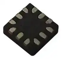
- No. of Pins: 12Pins
- Product Range: MMA
- Sensitivity Max: 1075counts/g
- Sensitivity Min: 973counts/g
- Sensitivity Typ: 1024counts/g
- Measurement Axis: X, Y, Z
- Sensor Case Style: QFN
- Acceleration Range: ± 8g
- MEMS Sensor Output: Digital
- Supply Voltage Max: 3.6V
- Supply Voltage Min: 1.95V
| Delivery and price | |
|---|---|
| Units per pack | 2500 |
| Price | 0.685 € |
| Current stock | 10+ |
| Lead time | 30 days |
**==> picture [86 x 78] intentionally omitted <==**

**----- Start of picture text -----**<br>
Se|<br>**----- End of picture text -----**<br>


## **MMA8491Q**

**3-Axis Multifunction Digital Accelerometer Rev. 2.1 — 26 April 2016**

**Data sheet: Technical data COMPANY PUBLIC**

## **1 General description**

The MMA8491Q is a low voltage, 3-axis low- _g_ accelerometer housed in a 3 mm x 3 mm QFN package. The device can accommodate two accelerometer configurations, acting as either a 45° tilt sensor or a digital output accelerometer with I[2] C bus.

- As a 45° tilt sensor, the MMA8491Q device offers extreme ease of implementation by using a single line output per axis.

- As a digital output accelerometer, the 14-bit ±8 _g_ accelerometer data can be read from the device with a 1 m _g_ /LSB sensitivity.

The extreme low power capabilities of the MMA8491Q will reduce the low data rate current consumption to less than 400 nA per Hz.

## **2 Features and benefits**

- Extreme low power, 400 nA per Hz

- Ultra-fast data output time, ~700 μs

- VDD supply range of 1.95 V to 3.6 V

- 3 mm x 3 mm, 0.65 mm pitch with visual solder joint inspection

- ±8 _g_ full-scale range

- 14-bit digital output, 1 m _g_ /LSB sensitivity

- Output Data Rate (ODR), implementation based from < 1 Hz to 800 Hz[1]

- I[2] C digital interface

- 3-axis, 45° tilt outputs

## **3 Typical applications**

- Smart grid: tamper detect

- Anti-theft

- White goods tilt

- Remote controls

1 The ODR for this device is user defined by the period of the Enable pulsed signal. The maximum recommended frequency of the Enable signal or the ODR that can be achieved for this device is 800 Hz.

**NXP Semiconductors**

**MMA8491Q**

**3-Axis Multifunction Digital Accelerometer**

## **4 Ordering information**

**Table 1. Ordering information**

|**Part Number**|**Temperature Range**|**Package**|**Shipping**|
|---|---|---|---|
|MMA8491QT|–40 to +85 °C|QFN 12|Tray|
|MMA8491QR1|–40 to +85 °C|QFN 12|1000 pc / Tape & Reel|
|MMA8491QR2|–40 to +85 °C|QFN 12|5000 pc / Tape & Reel|


## **5 Related documentation**

The MMA8491Q device features and operations are described in a variety of reference manuals, user guides, and application notes. To find the most current versions of these documents:

1. Go to the NXP homepage at: http://www.nxp.com/

2. In the Keyword search box at the top of the page, enter the device number MMA8491Q. In the Refine Your Result pane on the left, click on the Documentation link.

## **6 Block diagram**

**Figure 1. Block Diagram**

## **7 Pinout**

MMA8491Q is hosted in a 12-pin 3 mm x 3 mm QFN package. Ten pins are used for functions; two pins are unconnected. Refer to Table 2 for complete pin descriptions and functions.

MMA8491Q **Data sheet: Technical data COMPANY PUBLIC**

All information provided in this document is subject to legal disclaimers. **Rev. 2.1 — 26 April 2016**

© NXP B.V. 2016. All rights reserved

**2 / 28**

**NXP Semiconductors**

**MMA8491Q**

**3-Axis Multifunction Digital Accelerometer**

**==> picture [155 x 176] intentionally omitted <==**

**----- Start of picture text -----**<br>
MMA8491Q<br>Byp 1 10 Xout<br>VDD 2 9 Yout<br>SDA 3 8 Zout<br>EN 4 7 Gnd<br>Transparent top view<br>NC NC<br>12 11<br>5 6<br>SCL Gnd<br>**----- End of picture text -----**<br>


**Figure 2. Pin connection diagram**

**Table 2. Pin descriptions**

|**Pin**|**Symbol**|**Function**|**Description**|**Pin status**|
|---|---|---|---|---|
|1|Byp|Internal regulator<br>output capacitor<br>connection|The internal regulator voltage of 1.8 V is present on this<br>pin. Connect to external 0.1 μF bypass capacitor.|Output|
|2|VDD|Power Supply|Device power is supplied through the VDDline. Power<br>supply decoupling capacitors should be placed as near as<br>possible to pin 1 of the device.|Input|
|3|SDA|I2C Data|I2C Slave Data Line, open drain<br>**•** 7-bit I2C device address is 0x55<br>**•** The SDA and SCL I2C connections are open drain, and<br>therefore usually require a pull-up resistor|Input/Output|
|4|EN|Enable pin|The Enable pin fully turns on the accelerometer system<br>when it is pulled up to logic high. The accelerometer<br>system is turned off when the Enable pin is logic low.|Input|
|5|SCL|I2C Clock|I2C Slave Clock Line, open drain|Input|
|6|Gnd|Ground|Ground|Ground|
|7|Gnd|Ground|Ground|Ground|
|8|Zout|Push-pull Z-Axis<br>Tilt Detection<br>Output|**•** Output is high when acceleration is > 0.688_g_(axis is |<br>φ| > 45°).<br>**•** Output is low when acceleration is ≤ 0.688_g_(axis is |φ|<br>≤ 45°).<br>**•** These pins are push-pull output pins.|Output|
|9|Yout|Push-pull Y-Axis<br>Tilt Detection<br>Output||Output|
|10|Xout|Push-pull X-Axis<br>Tilt Detection<br>Output||Output|
|11|NC|No internal<br>connection|No internal connection||
|12|NC|No internal<br>connection|No internal connection||


All information provided in this document is subject to legal disclaimers.

MMA8491Q **Data sheet: Technical data COMPANY PUBLIC**

© NXP B.V. 2016. All rights reserved

**Rev. 2.1 — 26 April 2016**

**3 / 28**

**NXP Semiconductors**

**MMA8491Q**

**3-Axis Multifunction Digital Accelerometer**

## **8 Recommended application diagram**

**Figure 3. VDD connects to power supply and EN is pulsed**

To ensure the accelerometer is fully functional, connect the MMA8491Q as suggested in Figure 3.

- A capacitor must be connected to the Bypass pin (pin 1) to assist the internal voltage regulator. It is recommended to use a 0.1 μF capacitor. The capacitor should be placed as near as possible to the Bypass pin.

- The device power is supplied through the VDD line. The power supply decoupling capacitor should be placed as close as possible to the VDD pin.

- Use a 1.0 or 4.7 μF capacitor when the VDD and EN are not tied together.

- When VDD and EN are tied together, use a 0.1 μF capacitor. The 0.1 μF capacitor value has been chosen to minimize the average current consumption while still maintaining an acceptable level of power supply high frequency filtering.

- Both ground pins (pins 6 and 7) must be connected to ground.

- When the I[2] C communication line is used, use a pull-up resistor to connect to line SDA and SCL. The SCL line can be driven by a push-pull driver, in which case, no pull-up resistor is necessary. If SDA and SCL pins are not used, then they should be tied to ground.

## **9 Sensing direction and output response**

The MMA8491Q has three tilt detection outputs: Xout, Yout, and Zout. The following figure shows the output results at the six different orientation positions.

MMA8491Q **Data sheet: Technical data COMPANY PUBLIC**

All information provided in this document is subject to legal disclaimers. **Rev. 2.1 — 26 April 2016**

© NXP B.V. 2016. All rights reserved

**4 / 28**

**NXP Semiconductors**

**MMA8491Q**

**3-Axis Multifunction Digital Accelerometer**

**==> picture [351 x 254] intentionally omitted <==**

**----- Start of picture text -----**<br>
Top view  Side view<br>Portrait Up  Back<br>Pin 1<br>Xout @ 0  g<br>Gravity<br>Yout @ 0  g<br>Zout @ –1  g<br>Xout @ 0  g<br>Yout @ –1  g<br>Front<br>Landscape Left  Zout @ 0  g Landscape Right<br>Xout @ 0  g<br>Yout @ 0  g<br>Zout @ 1  g<br>Xout @ –1  g Xout @ 1  g Z<br>Yout @ 0  g Yout @ 0  g<br>Zout @ 0  g Portrait Down  Zout @ 0  g<br>X<br>Y<br>Xout @ 0  g<br>Yout @ 1  g<br>(Top view)<br>Zout @ 0  g Reference frame for acceleration measurement<br>**----- End of picture text -----**<br>


**Figure 4. Sensitive axes orientation and output response to ±1** _**g**_ **(gravity) stimulus**

## **10 Mechanical and electrical specifications**

## **10.1 Absolute maximum ratings**

Absolute maximum ratings are the limits the device can be exposed to without damage. Functional operation at absolute maximum rating is not guaranteed.

Although this device contains circuitry to protect against damage due to high static voltage or electrostatic fields, it is advised that normal precautions be taken to avoid application of any voltage higher than the maximum-rated voltage.

**Table 3. Absolute maximum ratings**

|**Symbol**|**Rating**|**Min**|**Max**|**Unit**|
|---|---|---|---|---|
|_g_max|Maximum acceleration (all axes, 100 μs)|—|10 000|V|
|VDD|Analog supply voltage|–0.3|3.6|V|
|Ddrop|Drop test|—|1.8|m|
|TAGOC|Operating temperature|–40|+85|°C|
|TSTG|Storage temperature|–40|+125|°C|


**Table 4. ESD and latch-up protection characteristics**

|**Symbol**|**Rating**|**Value**|**Unit**|
|---|---|---|---|
|VHBM|Human body model (HBM)|±2000|V|
|VMM|Machine model (MM)|±200|V|


All information provided in this document is subject to legal disclaimers.

© NXP B.V. 2016. All rights reserved

**Rev. 2.1 — 26 April 2016**

MMA8491Q **Data sheet: Technical data COMPANY PUBLIC**

**5 / 28**

**NXP Semiconductors**

**MMA8491Q**

**3-Axis Multifunction Digital Accelerometer**

|**Symbol**|**Rating**|**Value**|**Unit**|
|---|---|---|---|
|VCDM|Charge device model (CDM)|±500|V|
|ILU|Latch-up current at TA= 85 °C|±100|mA|


## **10.2 Mechanical characteristics**

## **Table 5. Accelerometer mechanical characteristics**

_VDD = 2.8 V, T = 25 °C, unless otherwise noted._

_Typical number is the target number, unless otherwise specified. All numbers are based on VDD cap = 4.7 μF._

|**Parameter**|**Symbol**|**Conditions**|**Min**|**Typ**|**Max**|**Unit**|
|---|---|---|---|---|---|---|
|Full-scale measurement range|FS[1]|—|—|±8|—|_g_|
|Sensitivity|So[2]|—|973|1024|1075|counts/_g_|
|Calibrated sensitivity error|CSE[2]|All axes, all ranges|–5|—|5|%|
|Cross-axis sensitivity|CXSEN<br>[1]|Die rotation included|–4.2|—|4.2|%|
|Sensitivity temperature variation|TCS[1]|–40 °C to +85 °C|–0.014|—|0.014|%/°C|
|Zero-_g_level temperature variation|TCO[1]|–40 °C to +85 °C|–0.98|—|0.98|m_g_/°C|
|Zero-_g_level offset accuracy|TyOff[2][3]|—|–100|—|100|m_g_|
|Zero-_g_level after board mount|TyOffPBM[1][4]|—|–120|—|120|m_g_|
|Noise|RMS[1]|—|—|11.5|18|m_g_-rms|
|Nonlinearity|NL[1]|—|—|—|1|%FS|
|Threshold /_g_-value[5]|TDL[6]|25 °C|0.583|0.688|0.780|_g_|
||TDL[1][4][6]|–40 °C to +85 °C|0.577|0.688|0.784||
|Threshold / Tilt angle[7]|TAGOC<br>[1]|25 °C|35.6|43.5|51.3|degrees|
|||–40 °C to +85 °C|35.2|43.5|51.7||
|Temperature range||—|–40|25|85|°C|


[1] Verified by characterization; not tested in production.

[2] Parameters tested 100% at final test at room temperature.

[3] Before board mount.

[4] Post-board mount offset specifications are based on a 4-layer PCB, relative to 25 °C.

[5] Internal threshold of output level change (from 0 _g_ reference), _g_ values are calculated from trip angles.

[6] All angles are based on the trip angle from static 0 _g_ to 1 _g_ ; the g-values are calculated from the trip angle.

[7] Internal threshold of output level change (from 0 _g_ reference).

MMA8491Q **Data sheet: Technical data COMPANY PUBLIC**

All information provided in this document is subject to legal disclaimers.

© NXP B.V. 2016. All rights reserved

**Rev. 2.1 — 26 April 2016**

**6 / 28**

**NXP Semiconductors**

**MMA8491Q**

**3-Axis Multifunction Digital Accelerometer**

## **10.3 Electrical characteristics**

## **Table 6. Electrical characteristics**

_VDD = 2.8 V, T = 25 °C, unless otherwise noted._

_Typical values represent mean or mean ±1 σ values, depending on the specific parameter. Typical number is the target number unless otherwise specified._

_All numbers are based on VDD cap = 4.7 μF._

|**Symbol**|**Parameter**|**Conditions**|**Min**|**Typ**|**Max**|**Unit**|
|---|---|---|---|---|---|---|
|VDD|Supply voltage[1]|—|1.71|1.8|3.6|V|
|IDD|Supply current in one-shot mode|VDD= 2.8 V, EN is<br>pulsed to VDDfor 1 ms|—|400[2][3][4]|980[1][5][6]|nA/Hz|
|ISD|Supply current in shutdown<br>mode|VDD= 2.8 V, EN = 0|—|1.8[2][3]|68[1][6]|nA|
|CBYP<br>[2]|Bypass capacitor at Byp pin|—|70|100|470|nF|
|VOH<br>[1]|High level output voltage Xout,<br>Yout, Zout|IO= 500 μA|0.85<br>* VDD|—|—|V|
|VOL<br>[1]|Low level output voltage Xout,<br>Yout, Zout|IO= 500 μA|—|—|0.15 * VDD|V|
|VIH<br>[1]|High level input voltage EN|VDD= 2.8 V|0.85<br>* VDD|—|—|V|
|VIL<br>[1]|Low level input voltage EN|VDD= 2.8 V|—|—|0.15 * VDD|V|
|VOLS<br>[7]|Low level output voltage SDA|IO= 3 mA|—|—|0.4|V|
|VIH<br>[7]|High level input voltage SDA,<br>SCL|VDD= 2.8 V|0.7 * VDD|—|—|V|
|VIL<br>[7]|Low level input voltage SDA,<br>SCL|VDD= 2.8 V|—|—|0.3 * VDD|V|
|ISOURCE<br>[1]|Output source current Xout,<br>Yout, Zout|Voltage high level<br>Vout = 0.85 x<br>VDD, VDD= 2.8 V|—|—|7.3|mA|
|ISINK<br>[1]|Output sink current Xout, Yout,<br>Zout|Voltage low level<br>Vout = 0.15 x<br>VDD, VDD= 2.8 V|—|—|8.9|mA|
|TON/<br>TACTIVE<br>[8]|Turn-on time<br>Measured from the time EN =<br>1.95 V to valid outputs|—|—|720[2][3][4]|900[1][5][6]|μs|
|TRST<br>[7]|Reset Time<br>The time between falling edge of<br>EN and next rising edge of EN|VDD= 2.8 V|1000|—|—|μs|


[1] Verified by characterization; not tested in production.

[2] Evaluation data: not tested in production.

[3] Typical number is mean data.

[4] Data is based on typical bypass cap = 100 nF.

[5] Data is based on max bypass cap = 470 nF.

[6] Over temperature -40 °C to 85 °C.

[7] Guaranteed by design.

[8] For application connection, see Figure 3

MMA8491Q **Data sheet: Technical data COMPANY PUBLIC**

All information provided in this document is subject to legal disclaimers.

© NXP B.V. 2016. All rights reserved

**Rev. 2.1 — 26 April 2016**

**7 / 28**

**NXP Semiconductors**

**MMA8491Q**

**3-Axis Multifunction Digital Accelerometer**

## **11 I[2] C Interface**

Acceleration data may be accessed through an I[2] C interface, thus making the device particularly suitable for direct interfacing with a microcontroller. The MMA8491Q features three interrupt signals that indicate the tilt-sensing results on X, Y, Z axis respectively. The raw accelerometer data are readable via I[2] C at the same time when an interrupt signal is available.

The registers embedded inside the MMA8491Q are accessible through the I[2] C serial interface, Table 7. To enable the I[2] C interface, the EN pin must be HIGH. If either EN or VDD are absent, the MMA8491Q I[2] C interface reads invalid data. The I[2] C interface may be used for communications along with other I[2] C devices. Removing power from the VDD pin of the MMA8491Q does not affect the I[2] C bus.

**Table 7. Serial interface pins**

|**Pin**|**Description**|
|---|---|
|SCL|I2C Serial Clock|
|SDA|I2C Serial Data|


There are two signals associated with the I[2] C bus; the Serial Clock Line (SCL) and the Serial Data Line (SDA). The SDA is a bidirectional line used for sending and receiving the data to/from the interface. External pull-up resistors connected to VDD are expected for SDA and SCL. When the bus is free both the lines are HIGH. The I[2] C interface is compliant with Fast mode (400 kHz, Table 8).

**Table 8. I[2] C slave timing values**

|**Parameter**|**Symbol**|**I2C Fast Mode[1]**|**I2C Fast Mode[1]**|**Unit**|
|---|---|---|---|---|
|||**Min**|**Max**||
|SCL clock frequency|fSCL|0|400|kHz|
|Bus-free time between STOP and START condition|tBUF|1.3|—|μs|
|(Repeated) START hold time|tHD;STA|0.6|—|μs|
|Repeated START setup time|tSU;STA|0.6|—|μs|
|STOP condition setup time|tSU;STO|0.6|—|μs|
|SDA data hold time|tHD;DAT|0.05|0.9[2]|μs|
|SDA setup time|tSU;DAT|100|—|μs|
|SCL clock low time|tLOW|1.3|—|μs|
|SCL clock high time|tHIGH|0.6|—|μs|
|SDA and SCL rise time|tr|20 + 0.1 Cb<br>[3]|300|μs|
|SDA and SCL fall time|tf|20 + 0.1 Cb<br>[3]|300|μs|
|SDA valid time[4]|tVD;DAT|—|0.9[2]|μs|
|SDA valid acknowledge time[5]|tVD;ACK|—|0.9[2]|μs|
|Pulse width of spikes on SDA and SCL that must be suppressed by<br>internal input filter|tSP|0|50|μs|
|Capacitive load for each bus line|Cb|—|400|pF|


[1] All values referred to VIH(min) (0.3VDD) and VIL(max) (0.7VDD) levels.

MMA8491Q All information provided in this document is subject to legal disclaimers.

© NXP B.V. 2016. All rights reserved

**Rev. 2.1 — 26 April 2016**

**Data sheet: Technical data COMPANY PUBLIC**

**8 / 28**

**NXP Semiconductors**

**MMA8491Q**

**3-Axis Multifunction Digital Accelerometer**

- [2] This device does not stretch the LOW period (tLOW) of the SCL signal.

- [3] Cb = total capacitance of one bus line in pF. [4] tVD;DAT = time for data signal from SCL LOW to SDA output (HIGH or LOW, depending on which one is worse). [5] tVD;ACK = time for Acknowledgement signal from SCL LOW to SDA output (HIGH or LOW, depending on which one is worse).

**Figure 5. I[2] C slave timing diagram**

## **11.1 I[2] C read operations**

The transaction on the bus is started through a start condition (START) signal. A START condition is defined as a HIGH-to-LOW transition on the data line while the SCL line is held HIGH.

After START has been transmitted by the Master, the bus is considered busy. The next byte of data transmitted after START contains the slave address in the first seven bits, and the eighth bit tells whether the Master is receiving data from the slave or transmitting data to the slave. When an address is sent, each device in the system compares the first seven bits after a start condition with its address. If they match, then the device considers itself addressed by the Master.

The ninth clock pulse, following the slave address byte, and each subsequent byte, is the acknowledge (ACK). The transmitter must release the SDA line during the ACK period. The receiver must then pull the data line LOW so that it remains stable low during the high period of the acknowledge clock period.

A LOW-to-HIGH transition on SDA while SCL is HIGH is defined as a stop condition (STOP). A data transfer is always terminated by a STOP.

A Master may also issue a repeated START during a data transfer. The MMA8491Q expects repeated STARTs to be used to randomly read from specific registers.

The MMA8491Q accelerometer standard 7-bit slave address is 01010101(0x55).

MMA8491Q **Data sheet: Technical data COMPANY PUBLIC**

All information provided in this document is subject to legal disclaimers.

© NXP B.V. 2016. All rights reserved

**Rev. 2.1 — 26 April 2016**

**9 / 28**

**NXP Semiconductors**

**MMA8491Q**

**3-Axis Multifunction Digital Accelerometer**

## **Table 9. I[2] C device address sequence**

|**Command**|**[7:1] Device**<br>**Address**|**[7:1] Device**<br>**Address**|**[0] R/W**|**[7:0] 8-bit**<br>**Final Value**|
|---|---|---|---|---|
|Read|01010101|0x55|1|0xAB|
|Write|01010101|0x55|0|0xAA|


## **11.1.1 Single-byte read**

The transmission of an 8-bit command begins on the falling edge of SCL. After the 8 clock cycles are used to send the command, note that the data returned is sent with the MSB first after the data is received. Figure 6 shows the timing diagram for the accelerometer 8-bit I[2] C read operation.

1. The Master (or MCU) transmits a start condition (ST) to the MMA8491Q, slave address (0x55), with the R/W bit set to “0” for a write, and the MMA8491Q sends an acknowledgement.

2. Then the Master (or MCU) transmits the address of the register to read and the MMA8491Q sends an acknowledgement.

3. The Master (or MCU) transmits a repeated start condition (SR) and then addresses the MMA8491Q (0x1D) with the R/ W bit set to 1 for a read from the previously selected register.

4. The Slave then acknowledges and transmits the data from the requested register.

5. The Master does not acknowledge (NAK) the transmitted data, but transmits a stop condition to end the data transfer.

## **11.1.2 Multiple-byte read**

When performing a multiple-byte read or _burst read_ , the MMA8491Q automatically increments the received register address commands after a read command is received. Therefore, after following the steps of a single-byte read, multiple bytes of data can be read from sequential registers after each MMA8491Q acknowledgment (AK) is received, until a no acknowledge (NAK) occurs from the Master, followed by a stop condition (SP) signaling an end of transmission.

MMA8491Q

All information provided in this document is subject to legal disclaimers. **Rev. 2.1 — 26 April 2016**

© NXP B.V. 2016. All rights reserved

**Data sheet: Technical data COMPANY PUBLIC**

**10 / 28**

**NXP Semiconductors**

**MMA8491Q**

**3-Axis Multifunction Digital Accelerometer**

## **11.1.3 I2C data sequence diagrams**

**==> picture [480 x 257] intentionally omitted <==**

**----- Start of picture text -----**<br>
Single-byte read<br>Device  Register  Device<br>Master ST W SR R NAK SP<br>Address[7:1] Address[7:0] Address[7:1]<br>Slave AK AK AK Data[7:0]<br>Multiple-byte read<br>Device  Register  Device<br>Master ST W SR R AK<br>Address[7:1] Address[7:0] Address[7:1]<br>Slave AK AK AK Data[7:0]<br>c o n t in u e d  . . .<br>Master AK AK NAK SP<br>Slave Data[7:0] Data[7:0] Data[7:0]<br>Legend<br>ST: Start Condition SP: Stop Condition NAK: No Acknowledge W: Write = 0<br>SR: Repeated Start Condition AK: Acknowledge R: Read = 1<br>**----- End of picture text -----**<br>


**Figure 6. I[2] C data sequence diagrams**

## **12 Modes of operation**

**==> picture [431 x 107] intentionally omitted <==**

**----- Start of picture text -----**<br>
EN = Low<br>One sample<br>VDD = On EN = High  is acquired<br>OFF*  SHUTDOWN  ACTIVE STANDBY<br>Mode Mode  Mode Mode<br>VDD = Off  VDD = On  VDD = On  VDD = On<br>EN = Don’t Care EN = Low  EN = High  EN = High<br>**----- End of picture text -----**<br>


*OFF mode can be entered from any state by removing the power.

**Figure 7. MMA8491Q operating modes**

**Table 10. MMA8491Q operating modes**

|**Mode**|**Conditions**|**Function description**|**Digital output state**|
|---|---|---|---|
|OFF|VDD= OFF<br>EN =_Don’t Care_|Device is powered off.|Hi-Z|
|SHUTDOWN|VDD= ON<br>EN = Low|All blocks are shut down.|Hi-Z|


© NXP B.V. 2016. All rights reserved

MMA8491Q **Data sheet: Technical data COMPANY PUBLIC**

All information provided in this document is subject to legal disclaimers.

**Rev. 2.1 — 26 April 2016**

**11 / 28**

**NXP Semiconductors**

**MMA8491Q**

**3-Axis Multifunction Digital Accelerometer**

|**Mode**|**Conditions**|**Function description**|**Digital output state**|
|---|---|---|---|
|ACTIVE|VDD= ON<br>EN = High|All blocks are enabled.<br>Device enters Standby mode automatically<br>after data conversion.|Deasserted, Xout = 0, Yout= 0, Zout = 0|
|STANDBY|VDD= ON<br>EN = High|Only digital output subsystem is enabled.<br>Data is valid and available only in this<br>stage.|Active, I2C outputs become valid|


## **12.1 ACTIVE mode**

The accelerometer subsystem is turned on at the rising edge of the EN pin, and acquires one sample for each of the three axes. Note that EN should not be asserted before VDD reaches 1.95 V. Samples are acquired, converted, and compensated for zero-g offset and gain errors, and then compared to an internal threshold value of 0.688 _g_ and stored.

- If any of the X, Y, Z axes sample’s **absolute value > this threshold** , then the corresponding outputs on these axes drive logic highs.

- If any of the X, Y, Z axes sample’s **absolute value ≤ this threshold** , then the corresponding outputs on these axes drive logic lows.

Read register 00h in this stage to determine whether the sample data is ready to be read.

## **12.2 STANDBY mode**

The device enters STANDBY mode automatically after the previously described function (powers into SHUTDOWN mode, ACTIVE mode) is accomplished. The digital output system outputs valid data, which can also be read via the I[2] C communication bus. This is the appropriate phase to read the measured data, either from the three push-pull logic outputs or through the I[2] C transaction. All other subsystems are turned off.

These outputs are held until the MMA8491Q operation mode changes. For lower power consumption, deassert the EN pin as soon as data is read (to enter SHUTDOWN mode).

## **12.3 Next sample acquisition**

The MMA8491Q needs to be brought back to the ACTIVE mode again by pulling EN pin up to a Logic 1. Another option is to power down the device and start from OFF mode as illustrated in Figure 7.

For applications where sampling intervals are greater than 30 seconds, the host can shut off the tilt sensor power after acquisition of tilt sensor output data to conserve energy and prolong battery life.

## **12.4 Power-up timing sequences**

The power-up timing sequence for MMA84591Q is shown in the following figure, where VDD is powered and the EN pin is activated to acquire a single sample. Additional samples can be acquired by repeating the EN pulse.

MMA8491Q **Data sheet: Technical data COMPANY PUBLIC**

All information provided in this document is subject to legal disclaimers.

© NXP B.V. 2016. All rights reserved

**Rev. 2.1 — 26 April 2016**

**12 / 28**

**NXP Semiconductors**

**MMA8491Q**

**3-Axis Multifunction Digital Accelerometer**

**==> picture [376 x 82] intentionally omitted <==**

**----- Start of picture text -----**<br>
OFF SHUTDOWN ACTIVE STANDBY SHUTDOWN<br>| | | |<br>VDD __d | | |<br>EN a a<br>||<br>Hi-Z Data<br>Data Available<br>|I tON<br>**----- End of picture text -----**<br>


## **Figure 8. MMA8491Q timing sequence**

tON is the time between EN to the end of ACTIVE stage, after which the newly acquired sample data is available.

## **12.5 45° tilt detection**

The output value changes according to the **absolute value** of the acceleration of the MMA8491Q compared to the threshold:

- When the acceleration’s **absolute value** > the threshold 0.688 _g_ , the output = 1.

- When the acceleration’s **absolute value** ≤ the threshold, the output = 0.

For example,

- When the MMA8491Q is set on a table, it senses 1 _g_ acceleration on Z-axis and senses 0 _g_ on X- and Y-axes.

- When the MMA8491Q is flipped upside down on the table, it senses –1 _g_ acceleration on Z-axis and senses 0 _g_ on X- and Y-axes.

In both cases Xout = 0, Yout = 0, and Zout = 1.

## **12.6 Tilt angle**

Tilt angles can be calculated from the _g_ -value threshold using the equation below. The tilt threshold is 0.688 _g_ , which corresponds to 43.5°. Figure 9 illustrates the tilt angle threshold.

Tilt Angle = asin (       )------------------- _g_ -value 1g

- When 0 _g_ acceleration is present on an axis, the tilt angle = 0°; when 1 _g_ acceleration is present on an axis, the tilt angle = 90°.

- When the tilt angle > the tilt threshold, the output for the axis is HIGH; when the tilt angle ≤ the tilt threshold, the output for the axis is LOW.

MMA8491Q **Data sheet: Technical data COMPANY PUBLIC**

All information provided in this document is subject to legal disclaimers. **Rev. 2.1 — 26 April 2016**

© NXP B.V. 2016. All rights reserved

**13 / 28**

**NXP Semiconductors**

**MMA8491Q**

## **3-Axis Multifunction Digital Accelerometer**

**==> picture [379 x 393] intentionally omitted <==**

**----- Start of picture text -----**<br>
Tilt Angle φ = 55°<br>Output = 1<br>Ø Horizontal<br>Reference<br>Projected g-value =<br>Threshold (g-value) = 0.688g<br>Threshold = 0.688g<br>1g<br>Ø<br>Ø  Horizontal  Horizontal<br>Reference  Reference<br>0.688g<br>0.688g<br>1g  1g<br>Tilt Angle φ = 30°  Tilt Angle φ = 70°<br>Output = 0  Output = 1<br>**----- End of picture text -----**<br>


**Figure 9. MMA8491Q output is based on tilt angle and sensor g-value**

MMA8491Q **Data sheet: Technical data COMPANY PUBLIC**

All information provided in this document is subject to legal disclaimers. **Rev. 2.1 — 26 April 2016**

© NXP B.V. 2016. All rights reserved

**14 / 28**

**NXP Semiconductors**

**MMA8491Q**

**3-Axis Multifunction Digital Accelerometer**

## **13 Register descriptions**

## **Table 11. Register address map**

|**Name**|**Type**|**Register**<br>**Address**|**Auto-**<br>**increment**<br>**Address[1]**|**Reset**|**Comment**|
|---|---|---|---|---|---|
|STATUS|R|0x00|0x01|0x00|Read time status|
|OUT_X_MSB|R|0x01|0x02|Output|[7:0] are the 8 MSBs of the 14-bit sample|
|OUT_X_LSB|R|0x02|0x03|Output|[7:2] are the 6 LSBs of the 14-bit sample|
|OUT_Y_MSB|R|0x03|0x04|Output|[7:0] are the 8 MSBs of the 14-bit sample|
|OUT_Y_LSB|R|0x04|0x05|Output|[7:2] are the 6 LSBs of the 14-bit sample|
|OUT_Z_MSB|R|0x05|0x06|Output|[7:0] are the 8 MSBs of the 14-bit sample|
|OUT_Z_LSB|R|0x06|**0x00**|Output|[7:2] are the 6 LSBs of the 14-bit sample|


[1] Auto-increment is the I[2] C feature that the I[2] C read address is automatically updated after each read. Auto-increment addresses that are not a simple increment are highlighted in bold. The auto-increment addressing is only enabled when device registers are read using I[2] C burst read mode. Therefore the internal storage of the auto-increment address is cleared whenever a stop-bit is detected.

## _**Notes:**_

- _Register contents are preserved when EN pin is set high after sampling._

- _Register contents are reset when EN pin is set low._

## **13.1 STATUS - Status register (address 00h)**

Register 0x00 reflects the real-time status information of the X, Y, and Z sample data. The data read bits (ZYXDR, ZDR, YDR, XDR) are set when samples are taken and ready to be read.

**Table 12. STATUS - Status register (address 00h) bit allocation**

|**Bit**|**7**||**6**|**5**|**4**|**3**|**2**|**1**|**0**|
|---|---|---|---|---|---|---|---|---|---|
|Symbol||||—||ZYXDR|ZDR|YDR|XDR|
|Reset|0||0|0|0|0|0|0|0|
|Access|R||R|R|R|R|R|R|R|
|**Table 13. STATUS -**||**Status register(address 00h) field descriptions**||||||||
|**Field**||**Description**||||||||
|3<br>ZYXDR||X-, Y-, Z-axis new Data Ready (and available)<br>**•** ZYXDR signals that a new sample for all channels is available.<br>**•** ZYXDR is cleared when the high-bytes of the acceleration data (OUT_X_MSB, OUT_Y_MSB,<br>OUT_Z_MSB) of all channels are read..<br>0: No new set of data ready (default value)<br>1: A new set of XYZ acceleration and temperature data is available||||||||
|2<br>ZDR||Z-axis new Data Ready (and available)<br>**•** ZDR is set whenever a new acceleration sample related to the Z-axis is generated.<br>**•** ZDR is cleared anytime OUT_Z_MSB register is read.<br>0: No new Z-axis data is ready (default value)<br>1: A new Z-axis data is ready||||||||


All information provided in this document is subject to legal disclaimers.

MMA8491Q **Data sheet: Technical data COMPANY PUBLIC**

© NXP B.V. 2016. All rights reserved

**Rev. 2.1 — 26 April 2016**

**15 / 28**

**NXP Semiconductors**

**MMA8491Q**

**3-Axis Multifunction Digital Accelerometer**

|**Field**|**Description**|
|---|---|
|1<br>YDR|Y-axis new Data Ready (and available)<br>**•** YDR is set whenever a new acceleration sample related to the Y-axis is generated.<br>**•** YDR is cleared anytime OUT_Y_MSB register is read.<br>0: No new Y-axis data ready (default value)<br>1: A new Y-axis data is ready|
|0<br>XDR|X-axis new Data Ready (and available)<br>**•** XDR is set whenever a new acceleration sample related to the X-axis is generated.<br>**•** XDR is cleared anytime OUT_X_MSB register is read.<br>0: No new X-axis data ready (default value)<br>1: A new X-axis data is ready|


## **13.2 Output data registers (addresses 01h to 06h)**

These registers contain the X-axis, Y-axis, and Z-axis14-bit output sample data (expressed as 2's complement numbers).

- OUT_X_MSB, OUT_X_LSB, OUT_Y_MSB, OUT_Y_LSB, OUT_Z_MSB, and OUT_Z_LSB are stored in the autoincrementing address range of 0x01 – 0x06.

- The LSB registers can only be read immediately following the read access of the corresponding MSB register. A random read access to the LSB registers is not possible.

- Reading the MSB register and then the LSB register in sequence ensures that both bytes (LSB and MSB) belong to the same data sample, even if a new data sample arrives between reading the MSB and the LSB byte.

- The accelerometer data registers should be read only after the status register has confirmed that new data on all axes is available.

**Table 14. OUT_X_MSB - Output data register (address 01h) bit allocation**

|**Bit**|**7**|**6**|**5**|**5**|**4**|**3**|**2**|**1**|**0**|
|---|---|---|---|---|---|---|---|---|---|
|Symbol|||||XD[13:6]|||||
|Reset|0|0|0||0|0|0|0|0|
|Access|R|R|R||R|R|R|R|R|
|**Table 15. OUT_X_LSB - Output data register(address 02h) bit allocation**||||||||||
|**Bit**|**7**|**6**|**5**|**4**||**3**|**2**|**1**|**0**|
|Symbol|||XD[5:0]|||||—|—|
|Reset|0|0|0|0||0|0|0|0|
|Access|R|R|R|R||R|R|R|R|


MMA8491Q **Data sheet: Technical data COMPANY PUBLIC**

All information provided in this document is subject to legal disclaimers.

© NXP B.V. 2016. All rights reserved

**Rev. 2.1 — 26 April 2016**

**16 / 28**

**NXP Semiconductors**

**MMA8491Q**

**3-Axis Multifunction Digital Accelerometer**

**Table 16. OUT_Y_MSB - Output data register (address 03h) bit allocation**

|**Bit**|**7**|**6**|**5**|**4**|**3**|**2**|**1**|**0**|
|---|---|---|---|---|---|---|---|---|
|Symbol||||YD[13:6]|||||
|Reset|0|0|0|0|0|0|0|0|
|Access|R|R|R|R|R|R|R|R|
|**Table 17. OUT_Y_LSB - Output data register(address 04h) bit allocation**|||||||||
|**Bit**|**7**|**6**|**5**|**4**|**3**|**2**|**1**|**0**|
|Symbol|||YD[13:6]||||—|—|
|Reset|0|0|0|0|0|0|0|0|
|Access|R|R|R|R|R|R|R|R|


**Table 18. OUT_Z_MSB - Output data register (address 05h) bit allocation**

|**Bit**|**7**|**6**|**5**|**4**|**3**|**2**|**1**|**0**|
|---|---|---|---|---|---|---|---|---|
|Symbol||||OUT_Z[7:0]|||||
|Reset|0|0|0|0|0|0|0|0|
|Access|R|R|R|R|R|R|R|R|
|**Table 19. OUT_Z_LSB - Output data register(address 06h) bit allocation**|||||||||
|**Bit**|**7**|**6**|**5**|**4**|**3**|**2**|**1**|**0**|
|Symbol|||ZD[5:0]||||—|—|
|Reset|0|0|0|0|0|0|0|0|
|Access|R|R|R|R|R|R|R|R|


## **13.3 Accelerometer output conversion**

**Table 20. Accelerometer output data**

|**14-bit Data**|**Range ±8****_g_ (1 m****_g_/count)**|
|---|---|
|01 1111 1111 1111|+8.000_g_|
|01 1111 1111 1110|+7.998_g_|
|...|...|
|00 0000 0000 0000|0.000_g_|
|11 1111 1111 1111|–0.001_g_|
|...|...|
|10 0000 0000 0001|–7.998_g_|
|10 0000 0000 0000|–8.000_g_|


All information provided in this document is subject to legal disclaimers.

© NXP B.V. 2016. All rights reserved

MMA8491Q **Data sheet: Technical data COMPANY PUBLIC**

**Rev. 2.1 — 26 April 2016**

**17 / 28**

**NXP Semiconductors**

**MMA8491Q**

**3-Axis Multifunction Digital Accelerometer**

## **14 Mounting guidelines**

Surface-mount printed circuit board (PCB) layout is a critical portion of the total design. The footprint for the surface mount package must be the correct size to ensure proper solder connection interface between the PCB and the package. With the correct footprint, the package will self-align when subjected to a solder reflow process. The purpose is to minimize the stress on the package after board mounting. The MMA8491Q accelerometers use the QFN package. This section describes suggested methods of soldering and mounting these devices to the PCB for consumer applications.

## **14.1 Overview of soldering considerations**

The information provided here is based on experiments executed on QFN devices. They do not represent exact conditions present at a customer site. Therefore, information herein should be used as guidance only, and process and design optimizations are recommended to develop an application specific solution. It should be noted that with the proper PCB footprint and solder stencil designs, the package will self-align during the solder reflow process.

## **14.2 Halogen content**

This package is designed to be Halogen Free, exceeding most industry and customer standards. Halogen Free means that no homogeneous material within the assembly package shall contain chlorine (Cl) in excess of 700 ppm or 0.07% weight/weight or bromine (Br) in excess of 900 ppm or 0.09% weight/weight.

## **14.3 PCB mounting recommendations**

- Do not solder down the six exposed pads under the package, thus minimizing boardmounting stress impact to product performance.

- PCB landing pad is 0.675 mm x 0.325 mm as shown in Figure 10.

- Solder mask opening = PCB land pad edge + 0.2 mm larger all around.

- Stencil opening size is 0.625 mm x 0.3 mm.

- Stencil thickness is 100 μm or 125 μm.

- The solder mask should not cover any of the PCB landing pads, as shown in Figure 10.

- No additional via nor metal pattern underneath package on the top of the PCB layer.

- Do not place any components or vias within 2 mm of the package land area. This may cause additional package stress if it is too close to the package land area.

- Signal traces connected to pads should be as symmetric as possible. Put dummy traces on NC pads, to have the same length of exposed trace for all pads.

- Use a standard pick-and-place process and equipment. Do not use a hand soldering process.

- Customers are advised to be cautious about the proximity of screw-down holes to the sensor, and the location of any press fit to the assembled PCB when in an enclosure. It is important that the assembled PCB remain flat after assembly to keep electronic operation of the device optimal.

- The PCB should be rated for the multiple lead-free reflow condition with a maximum 260 °C temperature.

- NXP sensors are compliant with Restrictions on Hazardous Substances (RoHS), having halide-free molding compound (green) and lead-free terminations. These

MMA8491Q **Data sheet: Technical data COMPANY PUBLIC**

All information provided in this document is subject to legal disclaimers.

© NXP B.V. 2016. All rights reserved

**Rev. 2.1 — 26 April 2016**

**18 / 28**

**NXP Semiconductors**

**MMA8491Q**

**3-Axis Multifunction Digital Accelerometer**

terminations are compatible with tin-lead (Sn-Pb) as well as tin-silver-copper (Sn-AgCu) solder paste soldering processes. Reflow profiles applicable to those processes can be used successfully for soldering the devices.

**Figure 10. PCB footprint guidelines**

MMA8491Q **Data sheet: Technical data COMPANY PUBLIC**

All information provided in this document is subject to legal disclaimers. **Rev. 2.1 — 26 April 2016**

© NXP B.V. 2016. All rights reserved

**19 / 28**

**NXP Semiconductors**

**MMA8491Q**

**3-Axis Multifunction Digital Accelerometer**

## **15 Package Information**

The MMA8491Q uses a 12-lead QFN package, case number 98ASA00290D.

## **15.1 Tape and reel information**

**==> picture [397 x 406] intentionally omitted <==**

**----- Start of picture text -----**<br>
Figure 11. Tape dimensions<br>Pin 1<br>Direction<br>to unreel<br>Barcode label<br>side of reel<br>Figure 12. Tape and reel orientation<br>**----- End of picture text -----**<br>


## **15.2 Package description**

This drawing is available for download at http://www.nxp.com/files/shared/doc/ package_info/98ASA00290D.pdf. Please consult the most recently issued drawing before initiating or completing a design.

MMA8491Q **Data sheet: Technical data COMPANY PUBLIC**

All information provided in this document is subject to legal disclaimers.

© NXP B.V. 2016. All rights reserved

**Rev. 2.1 — 26 April 2016**

**20 / 28**

**NXP Semiconductors**

**MMA8491Q**

**3-Axis Multifunction Digital Accelerometer**

**==> picture [326 x 369] intentionally omitted <==**

**==> picture [127 x 110] intentionally omitted <==**

**==> picture [48 x 53] intentionally omitted <==**

**==> picture [184 x 64] intentionally omitted <==**

**Figure 13. Case 2169-02, Issue X1, 12-Lead QFN—page 1**

All information provided in this document is subject to legal disclaimers.

© NXP B.V. 2016. All rights reserved

**Rev. 2.1 — 26 April 2016**

MMA8491Q

**Data sheet: Technical data COMPANY PUBLIC**

**21 / 28**

**NXP Semiconductors**

**MMA8491Q**

**3-Axis Multifunction Digital Accelerometer**

**==> picture [53 x 32] intentionally omitted <==**

**==> picture [48 x 55] intentionally omitted <==**

**==> picture [184 x 63] intentionally omitted <==**

**Figure 14. Case 2169-02, Issue X1, 12-Lead QFN—page 2**

All information provided in this document is subject to legal disclaimers.

© NXP B.V. 2016. All rights reserved

**Rev. 2.1 — 26 April 2016**

MMA8491Q

**Data sheet: Technical data COMPANY PUBLIC**

**22 / 28**

**NXP Semiconductors**

**MMA8491Q**

**3-Axis Multifunction Digital Accelerometer**

**==> picture [173 x 91] intentionally omitted <==**

**==> picture [48 x 54] intentionally omitted <==**

**==> picture [184 x 64] intentionally omitted <==**

**Figure 15. Case 2169-02, Issue X1, 12-Lead QFN—page 3**

All information provided in this document is subject to legal disclaimers.

MMA8491Q

© NXP B.V. 2016. All rights reserved

**Rev. 2.1 — 26 April 2016**

**Data sheet: Technical data COMPANY PUBLIC**

**23 / 28**

**NXP Semiconductors**

**MMA8491Q**

**3-Axis Multifunction Digital Accelerometer**

## **16 Revision history**

|**Revision**<br>**number**|**Revision**<br>**date**|**Description**|
|---|---|---|
|1.0|10/2012|**•** Initial release|
|2.0|11/2012|**•** Characterization data verified to be complete and final|
|2.1|4/2016|**•** Added MMA8491QR2 to Ordering information table<br>**•** Added paragraphs describing absolute maximum ratings<br>**•** Revised package dimensions drawings to the NXP format, no technical changes<br>**•** The format of this data sheet has been redesigned to comply with the new identity guidelines<br>of NXP Semiconductors<br>**•** Legal texts have been adapted to the new company name where appropriate|


MMA8491Q

All information provided in this document is subject to legal disclaimers.

© NXP B.V. 2016. All rights reserved

**Rev. 2.1 — 26 April 2016**

**Data sheet: Technical data COMPANY PUBLIC**

**24 / 28**

**NXP Semiconductors**

**MMA8491Q**

**3-Axis Multifunction Digital Accelerometer**

## **17 Legal information**

## **Data sheet status**

|**Document status[1]**|**Product status[2]**|**Definition**|
|---|---|---|
|Data sheet: Product preview|Development|This document contains information on a product<br>under development. NXP reserves the right to change<br>or discontinue this product without notice.|
|Data sheet: Advance information|Qualification|This document contains information on a pre-<br>production product. Specifications and pre-production<br>information herein are subject to change without<br>notice.|
|Data sheet: Technical data|Production|NXP reserves the right to change the production<br>detail specifications as may be required to permit<br>improvements in the design of its products.|


- [1] Please consult the most recently issued document before initiating or completing a design.

- [2] The product status of device(s) described in this document may have changed since this document was published and may differ in case of multiple devices. The latest product status information is available on the Internet at URL nxp.com.

**Definitions Disclaimers Draft —** The document is a draft version only. The content is still under internal review and subject to formal approval, which may result in modifications or additions. NXP Semiconductors does not give any representations or warranties as to the accuracy or completeness of information included herein and shall have no liability for the consequences of use of such information.

Information in this document is provided solely to enable system and software implementers to use NXP products. There are no express or implied copyright licenses granted hereunder to design or fabricate any integrated circuits based on the information in this document. NXP reserves the right to make changes without further notice to any products herein. NXP makes no warranty, representation, or guarantee regarding the suitability of its products for any particular purpose, nor does NXP assume any liability arising out of the application or use of any product or circuit, and specifically disclaims any and all liability, including without limitation consequential or incidental damages. “Typical” parameters that may be provided in NXP data sheets and/ or specifications can and do vary in different applications, and actual performance may vary over time. All operating parameters, including “typicals,” must be validated for each customer application by customer's technical experts. NXP does not convey any license under its patent rights nor the rights of others. NXP sells products pursuant to standard terms and conditions of sale, which can be found at the following address: nxp.com/salestermsandconditions.

## **Trademarks**

NXP, the NXP logo, Freescale, the Freescale logo and SMARTMOS are trademarks of NXP B.V. All other product or service names are the property of their respective owners.

MMA8491Q

All information provided in this document is subject to legal disclaimers.

© NXP B.V. 2016. All rights reserved

**Rev. 2.1 — 26 April 2016**

**Data sheet: Technical data COMPANY PUBLIC**

**25 / 28**

**NXP Semiconductors**

**MMA8491Q**

**3-Axis Multifunction Digital Accelerometer**

## **Tables**

|Tab.|1.|Ordering information ..........................................2|
|---|---|---|
|Tab.|2.|Pin descriptions .................................................3|
|Tab.|3.|Absolute maximum ratings ................................5|
|Tab.|4.|ESD and latch-up protection characteristics ......5|
|Tab.|5.|Accelerometer mechanical characteristics ........ 6|
|Tab.|6.|Electrical characteristics ....................................7|
|Tab.|7.|Serial interface pins .......................................... 8|
|Tab.|8.|I2C slave timing values .....................................8|
|Tab.|9.|I2C device address sequence .........................10|
|Tab.|10.|MMA8491Q operating modes ......................... 11|
|Tab.|11.|Register address map .....................................15|
|Tab.|12.|STATUS - Status register (address 00h) bit|
|||allocation ......................................................... 15|
|Tab.|13.|STATUS - Status register (address 00h) field|
|||descriptions ..................................................... 15|


- Tab. 14. OUT_X_MSB - Output data register (address 01h) bit allocation .............................16

- Tab. 15. OUT_X_LSB - Output data register (address 02h) bit allocation ............................................16

- Tab. 16. OUT_Y_MSB - Output data register (address 03h) bit allocation .............................17

- Tab. 17. OUT_Y_LSB - Output data register (address 04h) bit allocation ............................................17

- Tab. 18. OUT_Z_MSB - Output data register (address 05h) bit allocation .............................17

- Tab. 19. OUT_Z_LSB - Output data register (address 06h) bit allocation ............................................17

- Tab. 20. Accelerometer output data .............................. 17

MMA8491Q

All information provided in this document is subject to legal disclaimers. **Rev. 2.1 — 26 April 2016**

© NXP B.V. 2016. All rights reserved

**Data sheet: Technical data COMPANY PUBLIC**

**26 / 28**

**NXP Semiconductors**

**MMA8491Q**

**3-Axis Multifunction Digital Accelerometer**

## **Figures**

|Fig.|1.|Block Diagram ...................................................2|
|---|---|---|
|Fig.|2.|Pin connection diagram .....................................3|
|Fig.|3.|VDD connects to power supply and EN is|
|||pulsed ................................................................4|
|Fig.|4.|Sensitive axes orientation and output|
|||response to ±1 g (gravity) stimulus ................... 5|
|Fig.|5.|I2C slave timing diagram .................................. 9|
|Fig.|6.|I2C data sequence diagrams .......................... 11|
|Fig.|7.|MMA8491Q operating modes ......................... 11|
|Fig.|8.|MMA8491Q timing sequence ..........................13|


|Fig.|9.|MMA8491Q output is based on tilt angle and|
|---|---|---|
|||sensor g-value .................................................14|
|Fig.|10.|PCB footprint guidelines ..................................19|
|Fig.|11.|Tape dimensions .............................................20|
|Fig.|12.|Tape and reel orientation ................................20|
|Fig.|13.|Case 2169-02, Issue X1, 12-Lead QFN—|
|||page 1 ............................................................. 21|
|Fig.|14.|Case 2169-02, Issue X1, 12-Lead QFN—|
|||page 2 ............................................................. 22|
|Fig.|15.|Case 2169-02, Issue X1, 12-Lead QFN—|
|||page 3 ............................................................. 23|


MMA8491Q

All information provided in this document is subject to legal disclaimers. **Rev. 2.1 — 26 April 2016**

© NXP B.V. 2016. All rights reserved

**Data sheet: Technical data COMPANY PUBLIC**

**27 / 28**

**NXP Semiconductors**

**MMA8491Q**

**3-Axis Multifunction Digital Accelerometer**

## **Contents**

|**1**|**General description ............................................ 1**|
|---|---|
|**2**|**Features and benefits .........................................1**|
|**3**|**Typical applications ............................................1**|
|**4**|**Ordering information .......................................... 2**|
|**5**|**Related documentation ...................................... 2**|
|**6**|**Block diagram ..................................................... 2**|
|**7**|**Pinout ................................................................... 2**|
|**8**|**Recommended application diagram ..................4**|
|**9**|**Sensing direction and output response ............4**|
|**10**|**Mechanical and electrical specifications .......... 5**|
|10.1|Absolute maximum ratings ................................ 5|
|10.2|Mechanical characteristics .................................6|
|10.3|Electrical characteristics .................................... 7|
|**11**|**I2C Interface ........................................................ 8**|
|11.1|I2C read operations ...........................................9|
|11.1.1|Single-byte read .............................................. 10|
|11.1.2|Multiple-byte read ............................................ 10|
|11.1.3|I2C data sequence diagrams ...........................11|
|**12**|**Modes of operation ...........................................11**|
|12.1|ACTIVE mode ..................................................12|
|12.2|STANDBY mode ..............................................12|
|12.3|Next sample acquisition ...................................12|
|12.4|Power-up timing sequences ............................ 12|
|12.5|45° tilt detection ...............................................13|
|12.6|Tilt angle ..........................................................13|
|**13**|**Register descriptions ....................................... 15**|
|13.1|STATUS - Status register (address 00h) ......... 15|
|13.2|Output data registers (addresses 01h to 06h) .. 16|
|13.3|Accelerometer output conversion .................... 17|
|**14**|**Mounting guidelines ......................................... 18**|
|14.1|Overview of soldering considerations .............. 18|
|14.2|Halogen content .............................................. 18|
|14.3|PCB mounting recommendations .................... 18|
|**15**|**Package Information .........................................20**|
|15.1|Tape and reel information ............................... 20|
|15.2|Package description ........................................ 20|
|**16**|**Revision history ................................................ 24**|
|**17**|**Legal information ..............................................25**|


## **© NXP B.V. 2016. All rights reserved**

For more information, please visit: http://www.nxp.com For sales office addresses, please send an email to: salesaddresses@nxp.com **Released on 26 April 2016**
Updated at February 9, 2023
NXP Semiconductors is a global leader in secure connectivity solutions, driving innovation across the automotive, industrial, IoT, mobile, and communications infrastructure markets. By developing advanced, purpose-built technologies, NXP enables devices to sense, think, connect, and act intelligently, delivering rigorously tested components that make the connected world safer and more efficient. Within the semiconductor space, NXP is highly regarded for its extensive range of high-performance integrated circuits and discrete devices. The brand's portfolio excels in drivers and interfaces, featuring a comprehensive selection of I/O expanders designed to streamline complex system architectures. For demanding high-frequency and wireless applications, NXP provides industry-leading RF FETs and RF/PIN diodes engineered to deliver exceptional signal integrity, efficiency, and reliability. The NXP product lineup further extends to essential discrete components, including versatile bipolar transistors, JFETs, and small signal diodes optimized for precision switching and amplification. Additionally, the portfolio supports advanced automation and smart applications with precision IC sensors, such as MEMS accelerometers, alongside specialized power management solutions like AC/DC LED driver ICs and single MOSFETs for cutting-edge electronics design.
About Novapart
Novapart is a B2B electronic component broker specialising in stock shortages and cost reduction. We source hard-to-find parts and identify compliant alternatives across a catalogue of 410,000+ components from 500+ manufacturers.
Learn more →Stock Shortage Specialist
When a component is unavailable, discontinued or has an unacceptable lead time, we tap into our network of vetted European and Asian distributors to source what you need — without compromising on quality or traceability.
Request a quote →Compliant Alternatives
We identify pin-to-pin, electrically equivalent substitutes that meet the same certifications (RoHS, AEC-Q100, REACH) as your original specification — validated against datasheets, not just part numbers. Often at a lower cost.
BOM Analysis service →