
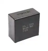


MKP1848H65070KY2
Power Film Capacitor, Metallized PP, Radial Box - 2 Pin, 50 µF, ± 10%, DC Link, Through Hole
- Manufacturer: VISHAY
- Product type: Power Film Capacitors
- ESR: 3900µohm
- SVHC: No SVHC (25-Jun-2025)
- Capacitance: 50µF
- Voltage(AC): -
- Voltage(DC): 700V
- Lead Spacing: 52.5mm
- Peak Current: 600A
- dv/dt Rating: 12V/µs
- Output (kvar): -
- Product Range: MKP1848H Series
- Product Width: 35mm
- Qualification: AEC-Q200
- Product Height: 50mm
- Product Length: 57.5mm
- Ripple Current: -
- Dielectric Type: Metallized PP
- Humidity Rating: GRADE III (Test Condition B)
- Product Diameter: -
- Capacitor Mounting: Through Hole
- RMS Current (Irms): 22.4A
- Capacitor Terminals: PC Pin
- Typical Applications: DC Link
- Capacitance Tolerance: ± 10%
- Capacitor Case / Package: Radial Box - 2 Pin
- Operating Temperature Max: 85°C
- Operating Temperature Min: -40°C
| Delivery and price | |
|---|---|
| Units per pack | 40 |
| Price | 11.2 € |
| Current stock | 10+ |
| Lead time | 30 days |
**MKP1848H DC-Link**

www.vishay.com

## Vishay Roederstein

## **THB Metallized Polypropylene DC-Link Film Capacitor 85 °C / 85 % RH 1000 h at UNDC - Automotive Grade**

## **FEATURES**

- High robustness under high humidity

- THB 85 °C, 85 % RH, 1000 h at rated UNDC

- AEC-Q200 qualified, revision D at Tmax. = 85 °C (Tmax. = 105 °C available on request)

- High ripple current capability, low ESR, low ESL

- Mounting: radial

- Material categorization: for definitions of compliance please see www.vishay.com/doc?99912

## **APPLICATIONS**

- Ideal for out-of-doors applications or in other harsh environments

- Renewable energies inverters

- UPS

- Battery chargers

- Motor drives

## **QUICK REFERENCE DATA**

|**QUICK REFERENCE DATA**|**QUICK REFERENCE DATA**|
|---|---|
|Rated capacitance range|1μF to 80μF|
|Capacitance tolerance|± 5 %, ± 10 %|
|Climatic testingclass|40 / 085 / 56|
|Rated temperature|85 °C|
|Maximumpermissible case temperature|105 °C, observingvoltage derating|
|Maximum applicablepeak topeak ripple voltage|0.2 x UNDC|
|Reference standards|IEC 61071, IEC 60068|
|Dielectric|Polypropylene film|
|Electrodes|Metallized dielectric capacitor|
|Construction|Mono construction|
|Encapsulation|Plastic case sealed with resin; flame retardant UL 94 V-0|
|Terminals|Tinned wire|
|Self inductance(LS)|< 1 nHper mm of lead spacing|
|WithstandingDC voltage between terminals(1)|1.5 UNDCfor 10 s, cut off current 10 mA, rise time≤1000 V/s|
|Insulation resistance|RC between leads, after 1 min > 10 000 s, measuringvoltage: 500 V|
|Life time expectancy(2)|Useful life time: > 100 000 h at UNDCand 70 °C<br>FIT: < 10 x 10-9/h (10 per 109component h) at 0.5 x UNDC, 40 °C|
|Marking|Manufacturer’s name; C-value; tolerance; rated voltage; manufacturer’s type designation;<br>code for dielectric material, manufacturer location,year and week|


## **Notes**

- For more detailed data and test requirements, contact dc-film@vishay.com

- For general information like characteristics and definitions used for film capacitors follow the link: www.vishay.com/doc?28147

- (1) See document “Voltage Proof Test for Metalized Film Capacitors” (www.vishay.com/doc?28169)

- (2) Statements about life time results from calculations which are based on internal tests. They have to be understood exclusively as estimations. Also due to external factors, the life time in the field application may deviate from the calculated life time

## **DC VOLTAGE RATINGS**

|UNDCat 85 °C|500 V|700 V|800 V|920 V|1200 V|
|---|---|---|---|---|---|
|UOPDCat 70 °C|600 V|800 V|960 V|1100 V|1440 V|
|UOPDCat 105 °C|350 V|450 V|560 V|650 V|850 V|


Revision: 04-Feb-2022

Document Number: 26078

**1**

For technical questions, contact: dc-film@vishay.com THIS DOCUMENT IS SUBJECT TO CHANGE WITHOUT NOTICE. THE PRODUCTS DESCRIBED HEREIN AND THIS DOCUMENT ARE SUBJECT TO SPECIFIC DISCLAIMERS, SET FORTH AT www.vishay.com/doc?91000

**MKP1848H DC-Link**

Vishay Roederstein

www.vishay.com

## **COMPOSITION OF CATALOG NUMBER**

**==> picture [476 x 238] intentionally omitted <==**

**----- Start of picture text -----**<br>
MULTIPLIER CAPACITANCE<br>(nF) (numerically)<br>10 4 Example: P1 PITCH<br>100 5 510 1000 nF 1 μF (mm) CODE<br>27.5 K<br>1000 6 610 10 000 nF 10 μF<br>37.5 P<br>10 000 7 710 100 000 nF 100 μF<br>52.5 Y<br>MKP 1848H 6 12 90 J P 4<br>TYPE CONSTRUCTION<br>SPECIAL CODE FOR TERMINAL<br>METALLIZED VOLTAGE TOLERANCE 2 2 pins<br>POLYPROPYLENE UNDC = 50 = 500 VDC J ± 5 % 4 4 pins P2 = 10.2 mm<br>UNDC = 70 = 700 VDC K ± 10 % 5 4 pins P2 = 20.3 mm<br>UNDC = 80 = 800 VDC (1) Customized<br>UNDC = 90 = 920 VDC<br>UNDC = 12 = 1200 VDC<br>**----- End of picture text -----**<br>


## **Note**

- (1) Tabs terminals or customized terminals are available on request

**==> picture [506 x 281] intentionally omitted <==**

**----- Start of picture text -----**<br>
DIMENSIONS  in millimeters<br>2 PINS<br>w I<br>h<br>P1<br>6 - 1<br>Ø dt P1 ± 0.4 - PCM 27.5 mm<br>P1 ± 0.5 - PCM ≥ 37.5 mm<br>4 PINS<br>I w<br>Marking<br>P2 P2<br>h<br>P1<br>6 - 2<br>Ø dt<br>P1 ± 0.5 P2 ± 0.5<br>**----- End of picture text -----**<br>


## **Note**

- Ø dt ± 10 % of standard diameter specified

Revision: 04-Feb-2022

Document Number: 26078

**2**

For technical questions, contact: dc-film@vishay.com THIS DOCUMENT IS SUBJECT TO CHANGE WITHOUT NOTICE. THE PRODUCTS DESCRIBED HEREIN AND THIS DOCUMENT ARE SUBJECT TO SPECIFIC DISCLAIMERS, SET FORTH AT www.vishay.com/doc?91000

**MKP1848H DC-Link**

www.vishay.com

## Vishay Roederstein

## **ELECTRICAL DATA AND ORDERING CODE**

|**ELECTRICAL DATA AND ORDERING CODE**|**ELECTRICAL DATA AND ORDERING CODE**|**ELECTRICAL DATA AND ORDERING CODE**|**ELECTRICAL DATA AND ORDERING CODE**|**ELECTRICAL DATA AND ORDERING CODE**|**ELECTRICAL DATA AND ORDERING CODE**|**ELECTRICAL DATA AND ORDERING CODE**|**ELECTRICAL DATA AND ORDERING CODE**|**ELECTRICAL DATA AND ORDERING CODE**|**ELECTRICAL DATA AND ORDERING CODE**|**ELECTRICAL DATA AND ORDERING CODE**|**ELECTRICAL DATA AND ORDERING CODE**|**ELECTRICAL DATA AND ORDERING CODE**|**ELECTRICAL DATA AND ORDERING CODE**|**ELECTRICAL DATA AND ORDERING CODE**|**ELECTRICAL DATA AND ORDERING CODE**|
|---|---|---|---|---|---|---|---|---|---|---|---|---|---|---|---|
|**UNDC**<br>**AT**<br>**85 °C**<br>**(V)**|**CAP.**<br>**(μF)**|**DIMENSION(5)**<br>**(mm)**|||**P1**<br>**(mm)**|**P2**<br>**(mm)**|**du/dt**<br>**(V/μs)**|**IPEAK**<br>**(A)**|**IRMS (2)**<br>**(A)**||**ESR(3)**<br>**10 kHz**<br>**(m**Ω**)**||**tan**δ **(4)**<br>**10 kHz**<br>**< (x 10-4)**||**ORDERING CODE(1)**|
|||**w**|**h**|**l**|||||**2**<br>**PINS**|**4**<br>**PINS**|**2**<br>**PINS**|**4**<br>**PINS**|**2**<br>**PINS**|**4**<br>**PINS**||
|500||**UOPDC AT 70 °C = 600 V; UOPDC AT 105 °C = 350 V**||||||||||||||
||5|15.0|25.0|32.0|27.5|-|40|200|7.0|-|10.1|-|65|-|MKP1848H55050+K2|
||6|15.0|25.0|32.0|27.5|-|40|240|7.6|-|8.6|-|65|-|MKP1848H56050+K2|
||7|18.0|28.0|32.0|27.5|-|40|280|8.8|-|7.6|-|65|-|MKP1848H57050+K2|
||8|18.0|28.0|32.0|27.5|-|40|320|9.3|-|6.8|-|65|-|MKP1848H58050+K2|
||10|21.0|31.0|32.0|27.5|-|40|400|11.0|-|5.7|-|65|-|MKP1848H61050+K2|
||12|21.0|31.0|32.0|27.5|-|40|480|11.7|-|5.0|-|65|-|MKP1848H61250+K2|
||15|22.0|38.0|32.0|27.5|-|40|600|13.9|-|4.3|-|65|-|MKP1848H61550+K2|
||20|21.5|38.5|42.0|37.5|10.2|20|400|13.6|14.4|5.3|4.8|145|130|MKP1848H62050+P*|
||22|21.5|38.5|42.0|37.5|10.2|20|440|14.1|14.8|5.0|4.5|145|130|MKP1848H62250+P*|
||25|21.5|38.5|42.0|37.5|10.2|20|500|14.7|15.5|4.6|4.1|145|130|MKP1848H62550+P*|
||30|30.0|45.0|42.0|37.5|10.2 / 20.3|20|600|18.1|19.1|4.1|3.7|145|130|MKP1848H63050+P*|
||35|30.0|45.0|42.0|37.5|10.2 / 20.3|20|700|18.9|19.9|3.8|3.4|145|130|MKP1848H63550+P*|
||40|30.0|45.0|42.0|37.5|10.2 / 20.3|20|800|19.6|20.7|3.5|3.2|145|130|MKP1848H64050+P*|
||45|30.0|45.0|42.0|37.5|10.2 / 20.3|20|900|20.2|21.3|3.3|3.0|145|130|MKP1848H64550+P*|
||50|30.0|45.0|57.5|52.5|20.3|10|500|20.9|22.0|3.9|3.5|250|225|MKP1848H65050+Y*|
||55|30.0|45.0|57.5|52.5|20.3|10|550|21.2|22.3|3.8|3.4|250|225|MKP1848H65550+Y*|
||60|30.0|45.0|57.5|52.5|20.3|10|600|21.4|22.5|3.7|3.3|250|225|MKP1848H66050+Y*|
||65|30.0|45.0|57.5|52.5|20.3|10|650|21.6|22.7|3.6|3.3|250|225|MKP1848H66550+Y*|
||70|35.0|50.0|57.5|52.5|20.3|10|700|23.5|24.8|3.6|3.2|250|225|MKP1848H67050+Y*|
||75|35.0|50.0|57.5|52.5|20.3|10|750|23.6|24.9|3.5|3.2|250|225|MKP1848H67550+Y*|
||80|35.0|50.0|57.5|52.5|20.3|10|800|23.8|25.1|3.5|3.2|250|225|MKP1848H68050+Y*|
|700||**UOPDC AT 70 °C = 800 V; UOPDC AT 105 °C = 450 V**||||||||||||||
||4|15.0|25.0|32.0|27.5|-|50|200|7.0|-|10.0|-|55|-|MKP1848H54070+K2|
||5|18.0|28.0|32.0|27.5|-|50|250|8.4|-|8.2|-|55|-|MKP1848H55070+K2|
||6|18.0|28.0|32.0|27.5|-|50|300|9.1|-|7.0|-|55|-|MKP1848H56070+K2|
||7|21.0|31.0|32.0|27.5|-|50|350|10.6|-|6.2|-|55|-|MKP1848H57070+K2|
||8|21.0|31.0|32.0|27.5|-|50|400|11.1|-|5.6|-|55|-|MKP1848H58070+K2|
||10|22.0|38.0|32.0|27.5|-|50|500|13.3|-|4.7|-|55|-|MKP1848H61070+K2|
||12|22.0|38.0|32.0|27.5|-|50|600|14.2|-|4.1|-|55|-|MKP1848H61270+K2|
||15|21.5|38.5|42.0|37.5|10.2|25|375|14.6|15.3|4.7|4.2|100|90|MKP1848H61570+P*|
||20|21.5|38.5|42.0|37.5|10.2|25|500|15.6|16.5|4.0|3.6|100|90|MKP1848H62070+P*|
||22|30.0|45.0|42.0|37.5|10.2 / 20.3|25|550|18.7|19.7|3.9|3.5|100|90|MKP1848H62270+P*|
||25|30.0|45.0|42.0|37.5|10.2 / 20.3|25|625|19.2|20.2|3.7|3.3|100|90|MKP1848H62570+P*|
||30|30.0|45.0|42.0|37.5|10.2 / 20.3|25|750|19.9|21.0|3.4|3.1|100|90|MKP1848H63070+P*|
||35|30.0|45.0|57.5|52.5|20.3|12|420|19.7|20.8|4.3|3.9|215|195|MKP1848H63570+Y*|
||40|30.0|45.0|57.5|52.5|20.3|12|480|20.1|21.2|4.2|3.8|215|195|MKP1848H64070+Y*|
||45|30.0|45.0|57.5|52.5|20.3|12|540|20.5|21.6|4.0|3.6|215|195|MKP1848H64570+Y*|
||50|35.0|50.0|57.5|52.5|20.3|12|600|22.4|23.6|3.9|3.5|215|195|MKP1848H65070+Y*|
||55|35.0|50.0|57.5|52.5|20.3|12|660|22.7|23.9|3.9|3.5|215|195|MKP1848H65570+Y*|
||60|35.0|50.0|57.5|52.5|20.3|12|720|22.9|24.1|3.8|3.4|215|195|MKP1848H66070+Y*|


Revision: 04-Feb-2022

Document Number: 26078

**3**

For technical questions, contact: dc-film@vishay.com THIS DOCUMENT IS SUBJECT TO CHANGE WITHOUT NOTICE. THE PRODUCTS DESCRIBED HEREIN AND THIS DOCUMENT ARE SUBJECT TO SPECIFIC DISCLAIMERS, SET FORTH AT www.vishay.com/doc?91000

**MKP1848H DC-Link**

www.vishay.com

## Vishay Roederstein

## **ELECTRICAL DATA AND ORDERING CODE**

|**ELECTRICAL DATA AND ORDERING CODE**|**ELECTRICAL DATA AND ORDERING CODE**|**ELECTRICAL DATA AND ORDERING CODE**|**ELECTRICAL DATA AND ORDERING CODE**|**ELECTRICAL DATA AND ORDERING CODE**|**ELECTRICAL DATA AND ORDERING CODE**|**ELECTRICAL DATA AND ORDERING CODE**|**ELECTRICAL DATA AND ORDERING CODE**|**ELECTRICAL DATA AND ORDERING CODE**|**ELECTRICAL DATA AND ORDERING CODE**|**ELECTRICAL DATA AND ORDERING CODE**|**ELECTRICAL DATA AND ORDERING CODE**|**ELECTRICAL DATA AND ORDERING CODE**|**ELECTRICAL DATA AND ORDERING CODE**|**ELECTRICAL DATA AND ORDERING CODE**|**ELECTRICAL DATA AND ORDERING CODE**|
|---|---|---|---|---|---|---|---|---|---|---|---|---|---|---|---|
|**UNDC**<br>**AT**<br>**85 °C**<br>**(V)**|**CAP.**<br>**(μF)**|**DIMENSION(5)**<br>**(mm)**|||**P1**<br>**(mm)**|**P2**<br>**(mm)**|**du/dt**<br>**(V/μs)**|**IPEAK**<br>**(A)**|**IRMS (2)**<br>**(A)**||**ESR(3)**<br>**10 kHz**<br>**(m**Ω**)**||**tan**δ **(4)**<br>**10 kHz**<br>**< (x 10-4)**||**ORDERING CODE(1)**|
|||**w**|**h**|**l**|||||**2**<br>**PINS**|**4**<br>**PINS**|**2**<br>**PINS**|**4**<br>**PINS**|**2**<br>**PINS**|**4**<br>**PINS**||
|800||**UOPDC AT 70 °C = 960 V; UOPDC AT 105 °C = 560 V**||||||||||||||
||3|15.0|25.0|32.0|27.5|-|60|180|6.3|-|12.3|-|50|-|MKP1848H53080+K2|
||4|18.0|28.0|32.0|27.5|-|60|240|7.7|-|9.8|-|50|-|MKP1848H54080+K2|
||5|21.0|31.0|32.0|27.5|-|60|300|9.1|-|8.4|-|50|-|MKP1848H55080+K2|
||6|21.0|31.0|32.0|27.5|-|60|360|9.7|-|7.4|-|50|-|MKP1848H56080+K2|
||7|21.0|31.0|32.0|27.5|-|60|420|10.1|-|6.7|-|50|-|MKP1848H57080+K2|
||8|22.0|38.0|32.0|27.5|-|60|480|11.6|-|6.2|-|50|-|MKP1848H58080+K2|
||10|22.0|38.0|32.0|27.5|-|60|600|12.3|-|5.4|-|50|-|MKP1848H61080+K2|
||12|21.5|38.5|42.0|37.5|10.2|30|360|11.8|12.5|7.1|6.4|100|90|MKP1848H61280+P*|
||15|21.5|38.5|42.0|37.5|10.2|30|450|12.8|13.5|6.1|5.5|100|90|MKP1848H61580+P*|
||20|30.0|45.0|42.0|37.5|10.2 / 20.3|30|600|16.3|17.2|5.1|4.6|100|90|MKP1848H62080+P*|
||22|30.0|45.0|42.0|37.5|10.2 / 20.3|30|660|16.8|17.7|4.8|4.3|100|90|MKP1848H62280+P*|
||25|30.0|45.0|42.0|37.5|10.2 / 20.3|30|750|17.4|18.3|4.5|4.0|100|90|MKP1848H62580+P*|
||30|30.0|45.0|57.5|52.5|20.3|15|450|17.4|18.3|5.6|5.0|210|190|MKP1848H63080+Y*|
||35|30.0|45.0|57.5|52.5|20.3|15|525|18.3|19.3|5.0|4.5|210|190|MKP1848H63580+Y*|
||40|35.0|50.0|57.5|52.5|20.3|15|600|20.7|21.8|4.6|4.2|210|190|MKP1848H64080+Y*|
||45|35.0|50.0|57.5|52.5|20.3|15|675|21.5|22.7|4.3|3.9|210|190|MKP1848H64580+Y*|
||50|35.0|50.0|57.5|52.5|20.3|15|750|22.2|23.4|4.0|3.6|210|190|MKP1848H65080+Y*|
|920||**UOPDC AT 70 °C = 1100 V; UOPDC AT 105 °C = 650 V**||||||||||||||
||2|15.0|25.0|32.0|27.5|-|65|130|5.7|-|15.2|-|40|-|MKP1848H52090+K2|
||3|18.0|28.0|32.0|27.5|-|65|195|7.4|-|10.8|-|40|-|MKP1848H53090+K2|
||4|18.0|28.0|32.0|27.5|-|65|260|8.3|-|8.5|-|40|-|MKP1848H54090+K2|
||5|21.0|31.0|32.0|27.5|-|65|325|9.8|-|7.2|-|40|-|MKP1848H55090+K2|
||6|22.0|38.0|32.0|27.5|-|65|390|11.5|-|6.3|-|40|-|MKP1848H56090+K2|
||7|22.0|38.0|32.0|27.5|-|65|455|12.1|-|5.6|-|40|-|MKP1848H57090+K2|
||8|22.0|38.0|32.0|27.5|-|65|520|12.6|-|5.2|-|40|-|MKP1848H58090+K2|
||10|21.5|38.5|42.0|37.5|10.2|35|350|11.8|12.4|7.2|6.4|90|80|MKP1848H61090+P*|
||12|30.0|45.0|42.0|37.5|10.2 / 20.3|35|420|14.6|15.4|6.3|5.7|90|80|MKP1848H61290+P*|
||15|30.0|45.0|42.0|37.5|10.2 / 20.3|35|525|15.7|16.5|5.5|4.9|90|80|MKP1848H61590+P*|
||20|30.0|45.0|42.0|37.5|10.2 / 20.3|35|700|17.0|18.0|4.7|4.2|90|80|MKP1848H62090+P*|
||22|30.0|45.0|57.5|52.5|20.3|18|396|16.3|17.2|6.4|5.7|150|135|MKP1848H62290+Y*|
||25|30.0|45.0|57.5|52.5|20.3|18|450|17.2|18.2|5.7|5.1|150|135|MKP1848H62590+Y*|
||30|30.0|45.0|57.5|52.5|20.3|18|540|18.5|19.5|4.9|4.4|150|135|MKP1848H63090+Y*|
||35|35.0|50.0|57.5|52.5|20.3|18|630|21.2|22.4|4.4|3.9|150|135|MKP1848H63590+Y*|
||40|35.0|50.0|57.5|52.5|20.3|18|720|22.3|23.5|4.0|3.6|150|135|MKP1848H64090+Y*|
|1200||**UOPDC AT 70 °C = 1440 V; UOPDC AT 105 °C = 850 V**||||||||||||||
||1|15.0|25.0|32.0|27.5|-|85|85|4.5|-|24.8|-|35|-|MKP1848H51012+K2|
||2|18.0|28.0|32.0|27.5|-|85|170|6.5|-|13.7|-|35|-|MKP1848H52012+K2|
||3|21.0|31.0|32.0|27.5|-|85|255|8.3|-|10.0|-|35|-|MKP1848H53012+K2|
||4|22.0|38.0|32.0|27.5|-|85|340|10.0|-|8.2|-|35|-|MKP1848H54012+K2|
||5|21.5|38.5|42.0|37.5|10.2|40|200|9.8|10.4|10.3|9.2|55|50|MKP1848H55012+P*|
||6|21.5|38.5|42.0|37.5|10.2|40|240|10.7|11.2|8.7|7.8|55|50|MKP1848H56012+P*|
||7|30.0|45.0|42.0|37.5|10.2 / 20.3|40|280|13.3|14.0|7.6|6.9|55|50|MKP1848H57012+P*|
||8|30.0|45.0|42.0|37.5|10.2 / 20.3|40|320|14.1|14.9|6.8|6.1|55|50|MKP1848H58012+P*|
||10|30.0|45.0|42.0|37.5|10.2 / 20.3|40|400|15.5|16.3|5.6|5.1|55|50|MKP1848H61012+P*|
||12|30.0|45.0|57.5|52.5|20.3|20|240|13.8|14.6|8.9|8.0|120|105|MKP1848H61212+Y*|
||15|30.0|45.0|57.5|52.5|20.3|20|300|15.2|16.0|7.3|6.6|120|105|MKP1848H61512+Y*|
||20|35.0|50.0|57.5|52.5|20.3|20|400|18.5|19.5|5.8|5.2|120|105|MKP1848H62012+Y*|
||22|35.0|50.0|57.5|52.5|20.3|20|440|19.2|20.2|5.4|4.8|120|105|MKP1848H62212+Y*|


## **Notes**

> (1) Change the “*” symbol with special code for the terminals and “+” for tolerance

> (2) Maximum RMS current at 10 kHz, +85 °C, Δt = +15 °C, capacitance tolerance ± 5 %, a typical ESR value at 10 kHz

> (3) Equivalent series resistance typical values at 10 kHz

- (4) Maximum tan δ values at 10 kHz

> (5) Standard dimensions, for maximum dimension please consult “Dimensions Tolerances”

Revision: 04-Feb-2022

**4**

Document Number: 26078

For technical questions, contact: dc-film@vishay.com THIS DOCUMENT IS SUBJECT TO CHANGE WITHOUT NOTICE. THE PRODUCTS DESCRIBED HEREIN AND THIS DOCUMENT ARE SUBJECT TO SPECIFIC DISCLAIMERS, SET FORTH AT www.vishay.com/doc?91000

**MKP1848H DC-Link**

www.vishay.com

## Vishay Roederstein

## **PACKAGING INFORMATION**

|**PACKAGING INFORMATION**|**PACKAGING INFORMATION**|**PACKAGING INFORMATION**|**PACKAGING INFORMATION**|**PACKAGING INFORMATION**|**PACKAGING INFORMATION**|**PACKAGING INFORMATION**|**PACKAGING INFORMATION**|**PACKAGING INFORMATION**|
|---|---|---|---|---|---|---|---|---|
|**UNDC**<br>**AT 85 °C**<br>**(V)**|**CAP.(1)**<br>**(μF)**|**DIMENSION**<br>**(mm)**|||**Ø dt**<br>**(mm)**|**ORDERING CODE(2)**|**MASS**<br>**(g)**|**SPQ(3)**<br>**(pcs)**|
|||**w**|**h**|**l**|||||
|500||**UOPDC AT 70 °C = 600 V; UOPDC AT 105 °C = 350 V**|||||||
||5|15.0|25.0|32.0|0.8|MKP1848H55050+K2|14.5|100|
||6|15.0|25.0|32.0|0.8|MKP1848H56050+K2|14.5|100|
||7|18.0|28.0|32.0|0.8|MKP1848H57050+K2|20.5|80|
||8|18.0|28.0|32.0|0.8|MKP1848H58050+K2|20.5|80|
||10|21.0|31.0|32.0|0.8|MKP1848H61050+K2|27.5|56|
||12|21.0|31.0|32.0|0.8|MKP1848H61250+K2|27|56|
||15|22.0|38.0|32.0|0.8|MKP1848H61550+K2|34|56|
||20|21.5|38.5|42.0|1.0|MKP1848H62050+P*|42.5|91|
||22|21.5|38.5|42.0|1.0|MKP1848H62250+P*|42|91|
||25|21.5|38.5|42.0|1.0|MKP1848H62550+P*|41|91|
||30|30.0|45.0|42.0|1.0|MKP1848H63050+P*|70.5|63|
||35|30.0|45.0|42.0|1.0|MKP1848H63550+P*|73|63|
||40|30.0|45.0|42.0|1.0|MKP1848H64050+P*|70.5|63|
||45|30.0|45.0|42.0|1.0|MKP1848H64550+P*|69.5|63|
||50|30.0|45.0|57.5|1.2|MKP1848H65050+Y*|95.5|45|
||55|30.0|45.0|57.5|1.2|MKP1848H65550+Y*|94|45|
||60|30.0|45.0|57.5|1.2|MKP1848H66050+Y*|91.5|45|
||65|30.0|45.0|57.5|1.2|MKP1848H66550+Y*|89.5|45|
||70|35.0|50.0|57.5|1.2|MKP1848H67050+Y*|127|40|
||75|35.0|50.0|57.5|1.2|MKP1848H67550+Y*|124.5|40|
||80|35.0|50.0|57.5|1.2|MKP1848H68050+Y*|120.5|40|
|700||**UOPDC AT 70 °C = 800 V; UOPDC AT 105 °C = 450 V**|||||||
||4|15.0|25.0|32.0|0.8|MKP1848H54070+K2|14.5|100|
||5|18.0|28.0|32.0|0.8|MKP1848H55070+K2|20.5|80|
||6|18.0|28.0|32.0|0.8|MKP1848H56070+K2|20|80|
||7|21.0|31.0|32.0|0.8|MKP1848H57070+K2|27|56|
||8|21.0|31.0|32.0|0.8|MKP1848H58070+K2|26.5|56|
||10|22.0|38.0|32.0|0.8|MKP1848H61070+K2|33.5|56|
||12|22.0|38.0|32.0|0.8|MKP1848H61270+K2|33.5|56|
||15|21.5|38.5|42.0|1.0|MKP1848H61570+P*|42|91|
||20|21.5|38.5|42.0|1.0|MKP1848H62070+P*|39|91|
||22|30.0|45.0|42.0|1.0|MKP1848H62270+P*|71|63|
||25|30.0|45.0|42.0|1.0|MKP1848H62570+P*|69|63|
||30|30.0|45.0|42.0|1.0|MKP1848H63070+P*|70|63|
||35|30.0|45.0|57.5|1.2|MKP1848H63570+Y*|91.5|45|
||40|30.0|45.0|57.5|1.2|MKP1848H64070+Y*|93.5|45|
||45|30.0|45.0|57.5|1.2|MKP1848H64570+Y*|90|45|
||50|35.0|50.0|57.5|1.2|MKP1848H65070+Y*|119|40|
||55|35.0|50.0|57.5|1.2|MKP1848H65570+Y*|123|40|
||60|35.0|50.0|57.5|1.2|MKP1848H66070+Y*|120|40|


Revision: 04-Feb-2022

Document Number: 26078

**5**

For technical questions, contact: dc-film@vishay.com THIS DOCUMENT IS SUBJECT TO CHANGE WITHOUT NOTICE. THE PRODUCTS DESCRIBED HEREIN AND THIS DOCUMENT ARE SUBJECT TO SPECIFIC DISCLAIMERS, SET FORTH AT www.vishay.com/doc?91000

**MKP1848H DC-Link**

www.vishay.com

## Vishay Roederstein

## **PACKAGING INFORMATION**

|**PACKAGING INFORMATION**|**PACKAGING INFORMATION**|**PACKAGING INFORMATION**|**PACKAGING INFORMATION**|**PACKAGING INFORMATION**|**PACKAGING INFORMATION**|**PACKAGING INFORMATION**|**PACKAGING INFORMATION**|**PACKAGING INFORMATION**|
|---|---|---|---|---|---|---|---|---|
|**UNDC**<br>**AT 85 °C**<br>**(V)**|**CAP.(1)**<br>**(μF)**|**DIMENSION**<br>**(mm)**|||**Ø dt**<br>**(mm)**|**ORDERING CODE(2)**|**MASS**<br>**(g)**|**SPQ(3)**<br>**(pcs)**|
|||**w**|**h**|**l**|||||
|800||**UOPDC AT 70 °C = 960 V; UOPDC AT 105 °C = 560 V**|||||||
||3|15.0|25.0|32.0|0.8|MKP1848H53080+K2|14.5|100|
||4|18.0|28.0|32.0|0.8|MKP1848H54080+K2|20.5|80|
||5|21.0|31.0|32.0|0.8|MKP1848H55080+K2|26.5|56|
||6|21.0|31.0|32.0|0.8|MKP1848H56080+K2|27|56|
||7|21.0|31.0|32.0|0.8|MKP1848H57080+K2|26.5|56|
||8|22.0|38.0|32.0|0.8|MKP1848H58080+K2|33|56|
||10|22.0|38.0|32.0|0.8|MKP1848H61080+K2|33|56|
||12|21.5|38.5|42.0|1.0|MKP1848H61280+P*|42|91|
||15|21.5|38.5|42.0|1.0|MKP1848H61580+P*|40.5|91|
||20|30.0|45.0|42.0|1.0|MKP1848H62080+P*|69|63|
||22|30.0|45.0|42.0|1.0|MKP1848H62280+P*|71|63|
||25|30.0|45.0|42.0|1.0|MKP1848H62580+P*|69.5|63|
||30|30.0|45.0|57.5|1.2|MKP1848H63080+Y*|89|45|
||35|30.0|45.0|57.5|1.2|MKP1848H63580+Y*|91.5|45|
||40|35.0|50.0|57.5|1.2|MKP1848H64080+Y*|119|40|
||45|35.0|50.0|57.5|1.2|MKP1848H64580+Y*|124|40|
||50|35.0|50.0|57.5|1.2|MKP1848H65080+Y*|119.5|40|
|920||**UOPDC AT 70 °C = 1100 V; UOPDC AT 105 °C = 650 V**|||||||
||2|15.0|25.0|32.0|0.8|MKP1848H52090+K2|15|100|
||3|18.0|28.0|32.0|0.8|MKP1848H53090+K2|20.5|80|
||4|18.0|28.0|32.0|0.8|MKP1848H54090+K2|20|80|
||5|21.0|31.0|32.0|0.8|MKP1848H55090+K2|27|56|
||6|22.0|38.0|32.0|0.8|MKP1848H56090+K2|34.5|56|
||7|22.0|38.0|32.0|0.8|MKP1848H57090+K2|34|56|
||8|22.0|38.0|32.0|0.8|MKP1848H58090+K2|33.5|56|
||10|21.5|38.5|42.0|1.0|MKP1848H61090+P*|42|91|
||12|30.0|45.0|42.0|1.0|MKP1848H61290+P*|77|63|
||15|30.0|45.0|42.0|1.0|MKP1848H61590+P*|74|63|
||20|30.0|45.0|42.0|1.0|MKP1848H62090+P*|69.5|63|
||22|30.0|45.0|57.5|1.2|MKP1848H62290+Y*|98|45|
||25|30.0|45.0|57.5|1.2|MKP1848H62590+Y*|94|45|
||30|30.0|45.0|57.5|1.2|MKP1848H63090+Y*|89.5|45|
||35|35.0|50.0|57.5|1.2|MKP1848H63590+Y*|124|40|
||40|35.0|50.0|57.5|1.2|MKP1848H64090+Y*|119.5|40|
|1200||**UOPDC AT 70 °C = 1440 V; UOPDC AT 105 °C = 850 V**|||||||
||1|15.0|25.0|32.0|0.8|MKP1848H51012+K2|15|100|
||2|18.0|28.0|32.0|0.8|MKP1848H52012+K2|20|80|
||3|21.0|31.0|32.0|0.8|MKP1848H53012+K2|26.5|56|
||4|22.0|38.0|32.0|0.8|MKP1848H54012+K2|33.5|56|
||5|21.5|38.5|42.0|1.0|MKP1848H55012+P*|42.5|91|
||6|21.5|38.5|42.0|1.0|MKP1848H56012+P*|41|91|
||7|30.0|45.0|42.0|1.0|MKP1848H57012+P*|76|63|
||8|30.0|45.0|42.0|1.0|MKP1848H58012+P*|74.5|63|
||10|30.0|45.0|42.0|1.0|MKP1848H61012+P*|70.5|63|
||12|30.0|45.0|57.5|1.2|MKP1848H61212+Y*|97.5|45|
||15|30.0|45.0|57.5|1.2|MKP1848H61512+Y*|92.5|45|
||20|35.0|50.0|57.5|1.2|MKP1848H62012+Y*|122.5|40|
||22|35.0|50.0|57.5|1.2|MKP1848H62212+Y*|119.5|40|


## **Notes**

- (1) Intermediate capacitance values available on request

> (2) Change the “*” symbol with special code for the terminals, and “+” for tolerance

> (3) SPQ = Standard Packing Quantity

Revision: 04-Feb-2022

Document Number: 26078

**6**

For technical questions, contact: dc-film@vishay.com THIS DOCUMENT IS SUBJECT TO CHANGE WITHOUT NOTICE. THE PRODUCTS DESCRIBED HEREIN AND THIS DOCUMENT ARE SUBJECT TO SPECIFIC DISCLAIMERS, SET FORTH AT www.vishay.com/doc?91000

**MKP1848H DC-Link**

www.vishay.com

Vishay Roederstein

## **CONSTRUCTION DESCRIPTION**

Low inductive wound cell elements of metallized polypropylene film, potted with resin in a flame retardant case.

## **SPECIFIC METHOD OF MOUNTING TO WITHSTAND VIBRATION AND SHOCK**

The capacitor unit is designed for mounting on a printed circuit board.

In order to withstand vibration and shock tests, it must be insured that the stand-off pips are in good contact with the printed circuit board.

The capacitors shall be mechanically fixed by the leads and the body clamped.

## **DIMENSIONS TOLERANCES**

For the maximum product dimensions for length (lmax.), width (wmax.), and height (hmax.) use the following tolerances:

lmax. = l + Δl, wmax. = w + Δw, and hmax. = h + Δh

Pitch = 27.5 mm, Δw = Δl = Δh = 0.7 mm

Pitch = 37.5 mm, Δw = Δl = Δh = 0.7 mm

Pitch = 52.5 mm, Δw = Δl = Δh = 1.0 mm

lmin. = l - Δl, wmin. = w - Δw, and hmin. = h - Δh

Pitch = 27.5 mm, Δw = Δl = Δh = 1.0 mm

Pitch = 37.5 mm, Δw = Δl = Δh = 1.0 mm

Pitch = 52.5 mm, Δw = Δl = Δh = 1.5 mm

## **SPACE REQUIREMENTS ON PRINTED-CIRCUIT BOARD**

For product height with seating plane as given by “IEC 60717” as reference.

## **For 2 pins:**

The maximum space for length (lmax.), width (wmax.), and height (hmax.) of film capacitors to take in account on the printed circuit board is shown in the drawings.

- For products with pitch ≤ 27.5 mm, Δw =  Δl = Δh = 0.7 mm

- For products with pitch = 37.5 mm, Δw = Δl = Δh = 0.7 mm

- For products with pitch = 52.5 mm, Δw = Δl = Δh = 1.0 mm

Eccentricity defined as in drawing. The maximum eccentricity is smaller than or equal to the lead diameter of the product concerned.

The maximum length and width of film capacitors is shown in the figure.

## **For 4 pins:**

**==> picture [228 x 258] intentionally omitted <==**

**----- Start of picture text -----**<br>
wmax. = w + Δw<br>Eccentricity<br>Imax. = I + ΔI<br>hmax. = h + Δh<br>Seating plane<br>P1<br>Ø D<br>P2 Wmax.<br>Lmax.<br>**----- End of picture text -----**<br>


Revision: 04-Feb-2022

**==> picture [6 x 7] intentionally omitted <==**

**----- Start of picture text -----**<br>
7<br>**----- End of picture text -----**<br>


Document Number: 26078

For technical questions, contact: dc-film@vishay.com THIS DOCUMENT IS SUBJECT TO CHANGE WITHOUT NOTICE. THE PRODUCTS DESCRIBED HEREIN AND THIS DOCUMENT ARE SUBJECT TO SPECIFIC DISCLAIMERS, SET FORTH AT www.vishay.com/doc?91000

**MKP1848H DC-Link**

www.vishay.com

Vishay Roederstein

|**P1 (mm)**|**Lmax. (mm)**|**Wmax. (mm)**|**Ø D (mm)**|Δ**h (mm)**|
|---|---|---|---|---|
|37.5|l + 1.5|w + 1.8|1.5|h + 0.7|
|52.5|l + 1.8|w + 2.0|1.7|h + 0.7|


## **SOLDERING CONDITIONS**

For general soldering conditions and wave soldering profile we refer to the document “Soldering Conditions Vishay Film Capacitors”: www.vishay.com/doc?26033

## **STORAGE TEMPERATURE**

Tstg = -25 °C to +35 °C with RH maximum 75 % without condensation.

## **RATINGS AND CHARACTERISTICS REFERENCE CONDITIONS**

Unless otherwise specified, all electrical values apply to an ambient temperature of 23 °C ± 1 °C, an atmospheric pressure of 86 kPa to 106 kPa, and a relative humidity of 50 % ± 2 %.

For reference testing, a conditioning period shall be applied over 96 h ± 4 h by heating the products in a circulating air oven at the rated temperature and a relative humidity not exceeding 20 %.

## **CHARACTERISTICS**

**==> picture [209 x 392] intentionally omitted <==**

**----- Start of picture text -----**<br>
4 10000<br>3<br>2<br>1<br>1000<br>0<br>-1<br>-2<br>100<br>-3<br>-4<br>-5<br>-6 10<br>-60 -40 -20 0 20 40 60 80 100 120<br>Tamb (°C)<br>Capacitance as a function of ambient temperature<br>(typical)<br>Axis Title<br>1.3 10000<br>1.2<br>70 °C<br>1.1<br>1000<br>1.0<br>85 °C<br>0.9<br>0.8<br>100<br>0.7<br>105 °C<br>0.6<br>0.5 10<br>1000  10 000  100 000 1 000 000<br>Lifetime Expectancy (h)<br>Lifetime expectancy by case temperature<br>(typical)<br>ΔC/C (%)<br> (V)<br>NDC<br> / U<br>OPDC<br>U<br>**----- End of picture text -----**<br>


**==> picture [229 x 392] intentionally omitted <==**

**----- Start of picture text -----**<br>
 100 000 10000<br>1000<br> 10 000<br>100<br>1000 10<br>0 20 40 60 80 100 120<br>Tamb (°C)<br>Insulation resistance as a function of ambient temperature<br>(typical)<br>Axis Title<br>1 000 000 10000<br>Pitch = 27.5 mm<br> 100 000<br>1 μF<br>3 μF<br> 10 000 5 μF 1000<br>1000<br>10 μF<br>100 15 μF 100<br>10<br>1 10<br>1 10 100 1000  10 000<br>f (kHz)<br>Impedance as a function of frequency<br>(typical)<br>RC (s) 1st line 2nd line<br>Z (mΩ) 1st line 2nd line<br>**----- End of picture text -----**<br>


Document Number: 26078

Revision: 04-Feb-2022

**8**

For technical questions, contact: dc-film@vishay.com THIS DOCUMENT IS SUBJECT TO CHANGE WITHOUT NOTICE. THE PRODUCTS DESCRIBED HEREIN AND THIS DOCUMENT ARE SUBJECT TO SPECIFIC DISCLAIMERS, SET FORTH AT www.vishay.com/doc?91000

**MKP1848H DC-Link**

## www.vishay.com

**==> picture [209 x 368] intentionally omitted <==**

**----- Start of picture text -----**<br>
 100 000 10000<br>Pitch = 37.5 mm<br> 10 000<br>5 μF<br>12 μF 1000<br>1000<br>45 μF<br>100 30 μF<br>100<br>25 μF<br>10<br>1 10<br>1 10 100 1000  10 000<br>f (kHz)<br>Impedance as a function of frequency<br>(typical)<br>Axis Title<br>100 10000<br>50 μF<br>80 μF 20 μF<br>45 μF 1000<br>10<br>15 μF<br>5 μF 100<br>1 10<br>1 10 100<br>f (kHz)<br>Z (mΩ)<br> (A)<br>IRMS<br>**----- End of picture text -----**<br>


Maximum IRMS current as function of frequency (500 VDC), based TA + 85 °C, Δt = +15 °C, capacitance tolerance ± 5 %, (typical curve)

**==> picture [209 x 160] intentionally omitted <==**

**----- Start of picture text -----**<br>
100 10000<br>30 μF<br>15 μF<br>60 μF<br>35 μF 1000<br>10 12 μF<br>4 μF 100<br>1 10<br>1 10 100<br>f (kHz)<br> (A)<br>IRMS<br>**----- End of picture text -----**<br>


Maximum IRMS current as function of frequency (700 VDC), based TA + 85 °C, Δt = +15 °C, capacitance tolerance ± 5 %, (typical curve)

## Vishay Roederstein

**==> picture [209 x 391] intentionally omitted <==**

**----- Start of picture text -----**<br>
 10 000 10000<br>Pitch = 52.5 mm<br>1000 35 μF<br>1000<br>50 μF<br>100<br>65 μF<br>80 μF 100<br>10<br>1 10<br>1 10 100 1000  10 000<br>f (kHz)<br>Impedance as a function of frequency<br>(typical)<br>Axis Title<br>100 10000<br>5 μF 50 μF 1000<br>80 μF<br>20 μF<br>10<br>100<br>45 μF<br>15 μF<br>1 10<br>1 10 100<br>f (kHz)<br>ESR as function of frequency (500 VDC)<br>(typical curve)<br>Z (mΩ)<br>ESR (mΩ)<br>**----- End of picture text -----**<br>


**==> picture [209 x 161] intentionally omitted <==**

**----- Start of picture text -----**<br>
100 10000<br>60 μF 1000<br>4 μF<br>10 15 μF<br>12 μF<br>100<br>30 μF<br>35 μF<br>1 10<br>1 10 100<br>f (kHz)<br>ESR (mΩ)<br>**----- End of picture text -----**<br>


**==> picture [140 x 17] intentionally omitted <==**

**----- Start of picture text -----**<br>
ESR as function of frequency (700 VDC)<br>(typical curve)<br>**----- End of picture text -----**<br>


Revision: 04-Feb-2022

Document Number: 26078

**9**

For technical questions, contact: dc-film@vishay.com THIS DOCUMENT IS SUBJECT TO CHANGE WITHOUT NOTICE. THE PRODUCTS DESCRIBED HEREIN AND THIS DOCUMENT ARE SUBJECT TO SPECIFIC DISCLAIMERS, SET FORTH AT www.vishay.com/doc?91000

**MKP1848H DC-Link**

## www.vishay.com

**==> picture [209 x 160] intentionally omitted <==**

**----- Start of picture text -----**<br>
100 10000<br>30 μF<br>50 μF<br>1000<br>25 μF<br>10<br>12 μF<br>10 μF 100<br>3 μF<br>1 10<br>1 10 100<br>f (kHz)<br> (A)<br>IRMS<br>**----- End of picture text -----**<br>


Maximum IRMS current as function of frequency (800 VDC), based TA + 85 °C, Δt = +15 °C, capacitance tolerance ± 5 %, (typical curve)

**==> picture [209 x 160] intentionally omitted <==**

**----- Start of picture text -----**<br>
100 10000<br>40 μF<br>1000<br>20 μF 22 μF<br>10<br>8 μF 10 μF<br>100<br>2 μF<br>1 10<br>1 10 100<br>f (kHz)<br> (A)<br>IRMS<br>**----- End of picture text -----**<br>


Maximum IRMS current as function of frequency (920 VDC), based TA + 85 °C, Δt = +15 °C, capacitance tolerance ± 5 %, (typical curve)

**==> picture [209 x 160] intentionally omitted <==**

**----- Start of picture text -----**<br>
100 10000<br>10 μF<br>22 μF 12 μF 1000<br>10<br>5 μF<br>4 μF<br>100<br>1 μF<br>1 10<br>1 10 100<br>f (kHz)<br> (A)<br>IRMS<br>**----- End of picture text -----**<br>


Maximum IRMS current as function of frequency (1200 VDC), based TA + 85 °C, Δt = +15 °C, capacitance tolerance ± 5 %, (typical curve)

Revision: 04-Feb-2022

## Vishay Roederstein

**==> picture [209 x 377] intentionally omitted <==**

**----- Start of picture text -----**<br>
100 10000<br>3 μF 50 μF 1000<br>30 μF<br>10 12 μF<br>10 μF 100<br>25 μF<br>1 10<br>1 10 100<br>f (kHz)<br>ESR as function of frequency (800 VDC)<br>(typical curve)<br>Axis Title<br>100 10000<br>40 μF<br>2 μF 1000<br>10 μF<br>22 μF<br>10<br>20 μF 8 μF 100<br>1 10<br>1 10 100<br>f (kHz)<br>ESR (mΩ)<br>ESR (mΩ)<br>**----- End of picture text -----**<br>


ESR as function of frequency (920 VDC) (typical curve)

**==> picture [209 x 160] intentionally omitted <==**

**----- Start of picture text -----**<br>
100 10000<br>1 μF<br>4 μF 1000<br>5 μF<br>10<br>22 μF 10 μF 100<br>12 μF<br>1 10<br>1 10 100<br>f (kHz)<br>ESR (mΩ)<br>**----- End of picture text -----**<br>


ESR as function of frequency (1200 VDC) (typical curve)

Document Number: 26078

**10**

For technical questions, contact: dc-film@vishay.com THIS DOCUMENT IS SUBJECT TO CHANGE WITHOUT NOTICE. THE PRODUCTS DESCRIBED HEREIN AND THIS DOCUMENT ARE SUBJECT TO SPECIFIC DISCLAIMERS, SET FORTH AT www.vishay.com/doc?91000

**MKP1848H DC-Link**

**==> picture [77 x 10] intentionally omitted <==**

**----- Start of picture text -----**<br>
www.vishay.com<br>**----- End of picture text -----**<br>


## Vishay Roederstein

**==> picture [475 x 183] intentionally omitted <==**

**----- Start of picture text -----**<br>
1.6 10000 35 10000<br>1.4 30<br>1.2<br>25<br>1000 1000<br>1.0<br>20<br>0.8<br>15<br>0.6<br>100 100<br>10<br>0.4<br>0.2 5<br>0 10 0 10<br>45 65 85 105 125 45 65 85 105 125<br>Maximum Ambient Temperature (°C) Maximum Ambient Temperature (°C)<br>Maximum IRMS current in function of the ambient temperature Maximum allowed component temperature rise (ΔT)<br>as a function of ambient temperature (Tamb)<br> max.<br>RMS<br>ΔT<br> Operational / I 1st line 2nd line 2nd line<br>IRMS<br>**----- End of picture text -----**<br>


## **HEAT CONDUCTIVITY**

|**HEAT CONDUCTIVITY**|**HEAT CONDUCTIVITY**|**HEAT CONDUCTIVITY**|**HEAT CONDUCTIVITY**|
|---|---|---|---|
|**DIMENSIONS(mm)**|||**HEAT CONDUCTIVITY**<br>**(mW/°C)**|
|**w**|**h**|**l**||
|15.0|25.0|32.0|33|
|18.0|28.0|32.0|39|
|21.0|31.0|32.0|46|
|22.0|38.0|32.0|55|
|21.5|38.5|42.0|66|
|30.0|45.0|42.0|90|
|30.0|45.0|57.5|113|
|35.0|50.0|57.5|132|


## **POWER DISSIPATION AND MAXIMUM COMPONENT TEMPERATURE RISE**

The power dissipation must be limited in order not to exceed the maximum allowed component temperature rise as a function of the free air ambient temperature.

The power dissipation can be calculated according type detail specification www.vishay.com/doc?28147

The component temperature rise (ΔT) can be measured (see section “Measuring the Component Temperature” for more details) or calculated by ΔT = P/G:

- ΔT = TC - Tamb = case temperature rise (°C) with a maximum of 15 °C at rated temperature

- P = IRMS[2] x ESR = power dissipation of the component (mW)

- G = heat conductivity of the component (mW/°C)

## **MEASURING THE COMPONENT TEMPERATURE**

**==> picture [46 x 8] intentionally omitted <==**

**----- Start of picture text -----**<br>
Thermocouple<br>**----- End of picture text -----**<br>


The case temperature is measured in unloaded condition (Tamb) and loaded condition (TC). The temperature rise is given by ΔT = TC - Tamb

To avoid external thermal radiation or convection, the capacitor must be tested in a closed area, free from air circulation.

Revision: 04-Feb-2022

Document Number: 26078

**11**

For technical questions, contact: dc-film@vishay.com THIS DOCUMENT IS SUBJECT TO CHANGE WITHOUT NOTICE. THE PRODUCTS DESCRIBED HEREIN AND THIS DOCUMENT ARE SUBJECT TO SPECIFIC DISCLAIMERS, SET FORTH AT www.vishay.com/doc?91000

**MKP1848H DC-Link**

www.vishay.com

Vishay Roederstein

## **APPLICATION NOTES AND LIMITING CONDITIONS**

These capacitors are not suitable for mains applications as across-the-line capacitors without additional protection.

These mains applications are strictly regulated in safety standards and therefore electromagnetic interference suppression capacitors conforming the standards must be used.

To select the capacitor for a certain application, the following conditions must be checked:

1. The continuous peak voltage (UP+) shall not exceed the DC voltage rating (UNDC)

2. The peak-to-peak ripple voltage (UPP) shall not be greater than 0.2 x (UNDC)

**==> picture [183 x 89] intentionally omitted <==**

**----- Start of picture text -----**<br>
Non reversing recurrent waveform<br>Up+, UNDC<br>Up-<br>t<br>Voltage (V)<br>**----- End of picture text -----**<br>


3. For capacitors connected in parallel, normally the proof voltage and possibly the rated voltage must be reduced. For information depending of the capacitance value and the number of parallel connections contact: dc-film@vishay.com

4. The voltage peak slope (du/dt) shall not exceed the pulse slope at the DC voltage rating.

   - If the pulse voltage is lower than the rated DC voltage, the rated voltage pulse slope may be multiplied by UNDC and divided by the applied voltage.

For all other pulses following equation must be fulfilled:

**==> picture [142 x 35] intentionally omitted <==**

T is the pulse duration

|**MAXIMUM REPETITIVE PEAK VOLTAGES**|**MAXIMUM REPETITIVE PEAK VOLTAGES**|
|---|---|
|**REPETITIVE SURGE VOLTAGE**|**MAXIMUM DURATION PER DAY**|
|1.1 x UNDC|30 % on load duration|
|1.15 x UNDC|30 min|
|1.2 x UNDC|5 min|
|1.3 x UNDC|1 min|
|1.5 x UNDC|110 ms|


## **Note**

- The capacitor unit may be subjected to the surge above without any significant reduction of lifetime expectancy

Revision: 04-Feb-2022

Document Number: 26078

**12** For technical questions, contact: dc-film@vishay.com THIS DOCUMENT IS SUBJECT TO CHANGE WITHOUT NOTICE. THE PRODUCTS DESCRIBED HEREIN AND THIS DOCUMENT ARE SUBJECT TO SPECIFIC DISCLAIMERS, SET FORTH AT www.vishay.com/doc?91000

**MKP1848H DC-Link**

www.vishay.com

Vishay Roederstein

|**TEST CONDITIONS AND REQUIREMENTS ACCORDING IEC 61071**|**TEST CONDITIONS AND REQUIREMENTS ACCORDING IEC 61071**|**TEST CONDITIONS AND REQUIREMENTS ACCORDING IEC 61071**|**TEST CONDITIONS AND REQUIREMENTS ACCORDING IEC 61071**|**TEST CONDITIONS AND REQUIREMENTS ACCORDING IEC 61071**|
|---|---|---|---|---|
|**SUB-CLAUSE NUMBER AND TEST**|**CONDITIONS**|||**PERFORMANCE REQUIREMENTS**|
|**ROUTINE TEST - FINAL INSPECTION**|||||
|5.14.2-1<br>External inspection,<br>visual examination<br>5.14.2-2<br>Dimensions<br>5.3-1<br>Capacitance<br>5.3-2<br>tanδ<br>5.5.1-2<br>DC voltage test between terminals<br>5.7<br>Insulation resistance|1 kHz at room temperature<br>10 kHz at room temperature<br>1.5 x UNDCat Tamb<br>Duration: 10 s<br>Measuring voltage 500 V at room temperature<br>Duration: 1 min|||Legible marking as specified<br>See specification drawing<br>See specific reference data<br>See specific reference data<br>No visible damage or puncture<br>No flashover<br>See specific reference data|
|**TYPE TESTS**|||||
|5.14.2<br>External inspection<br>5.14.0<br>Initial measurements<br>5.14.1-1/4 Robustness of terminations<br>IEC 60068-2-21<br>5.14.1-6<br>Resistance to soldering heat<br>IEC 60068-2-20<br>5.14.4<br>Final measurements|Check for finish, marking, and overall<br>dimensions<br>Capacitance at 1 kHz<br>tanδat 10 kHz<br>Tensile Ua1: duration: 10 s ± 1 s|||Legible marking and finish as specified<br>Dimensions: see specific drawing<br>|ΔC/C|≤0.5 %<br>Increase of tanδ ≤0.0050<br>Compared to values measured in 5.14.0|
||Wire diameter|Section|Load||
||d≤0.80 mm|S≤0.5 mm2|10 N (± 10 %)||
||d≤1.25 mm|S≤1.2 mm2|20 N (± 10 %)||
||Bending, Ub method 1: 4 x 90 °,<br>duration 2 s to 3 s/bend||||
||Wire diameter|Section|Load||
||d≤0.80 mm|Zx ≤0.050 mm3|5 N (± 10 %)||
||d≤1.25 mm|Zx ≤0.019 mm3|10 N (± 10 %)||
||No predrying, method 1A<br>Solder bath: 280 °C ± 5 °C<br>Duration: 10 s ± 1 s<br>Capacitance<br>tanδ||||
|5.14.0<br>Initial measurements<br>5.14.3-1<br>Vibration<br>IEC 60068-2-6<br>5.14.3-2<br>Shock or impact<br>IEC 60068-2-6<br>5.14.4<br>Final measurements|Capacitance at 1 kHz<br>tanδat 10 kHz<br>10 Hz to 55 Hz: amplitude ± 0.35 mm or<br>acceleration 98 m/s2<br>Test duration: 10 frequency cycles<br>(3 axes offset from each other by 90°)<br>1 octave/min<br>Visual examination<br>Pulse shape: half sine<br>Acceleration: 490 m/s2<br>Duration of pulse: 11 ms<br>Visual examination<br>Capacitance<br>tanδ|||No visible damage<br>No visible damage<br>|ΔC/C|≤0.5 %<br>Increase of tanδ ≤0.0050<br>Compared to values measured in 5.14.0|


Revision: 04-Feb-2022

Document Number: 26078

**13**

For technical questions, contact: dc-film@vishay.com THIS DOCUMENT IS SUBJECT TO CHANGE WITHOUT NOTICE. THE PRODUCTS DESCRIBED HEREIN AND THIS DOCUMENT ARE SUBJECT TO SPECIFIC DISCLAIMERS, SET FORTH AT www.vishay.com/doc?91000

**MKP1848H DC-Link**

www.vishay.com

Vishay Roederstein

|**TEST CONDITIONS AND REQUIREMENTS ACCORDING IEC 61071**|**TEST CONDITIONS AND REQUIREMENTS ACCORDING IEC 61071**|**TEST CONDITIONS AND REQUIREMENTS ACCORDING IEC 61071**|
|---|---|---|
|**SUB-CLAUSE NUMBER AND TEST**|**CONDITIONS**|**PERFORMANCE REQUIREMENTS**|
|**TYPE TESTS**|||
|5.5.3-1 Initial measurements<br>5.5.3-2 DC voltage test between terminals<br>5.5.3-3 Final measurements|Capacitance at 1 kHz<br>tanδat 10 kHz<br>Insulation resistance<br>1.5 x UNDCat Tamb<br>Duration: 60 s<br>Capacitance<br>tanδ <br>Insulation resistance||ΔC/C|≤0.5 %<br>Increase of tanδ ≤0.0050<br>IR≥50 % of specified values|
|5.9-1<br>Initial measurements<br>5.9-2<br>Surge discharge test<br>5.9-2<br>DC voltage test between terminals<br>5.9-3<br>Final measurements|Capacitance at 1 kHz<br>tanδat 10 kHz<br>Insulation resistance<br>1.1 x UNDC<br>Number of discharges: 5<br>Time lapse: every 2 min (10 min total)<br>Within 5 min after the surge discharge test<br>1.5 x UNDCat Tamb<br>Duration: 60 s<br>Capacitance<br>tanδ<br>Insulation resistance||ΔC/C|≤1.0 %<br>tanδ ≤1.2 x initial tanδ+ 0.0001<br>Compared to values measured in 5.9-1<br>IR≥50 % of specified values|
|5.11-1 Initial measurements<br>5.11-2 Self healing test<br>5.11-3 Final measurements|Capacitance at 1 kHz<br>tanδat 10 kHz<br>Insulation resistance<br>1.5 x UNDC<br>Duration: 10 s<br>increase the voltage at 100 V/s till 5 clearings<br>occur or until voltage reach max. of 2.5 x UNDC<br>for a duration of 10 s<br>Capacitance<br>tanδ<br>Insulation resistance|Number of clearings≤5<br>Clearing = voltage drop of 5 %<br>|ΔC/C|≤0.5 %<br>tanδ ≤1.2 x initial tanδ+ 0.0001<br>Compared to values measured in 5.11.1<br>IR≥50 % of specified values|
|5.13-0 Initial measurements<br>5.13-1 Change of temperature<br>acc. to IEC 60068-2-14<br>5.13.2 Damp heat steady state<br>acc. to IEC 60068-2-78<br>5.5.3-2 DC voltage test between terminals<br>5.13.3 Final measurements|Capacitance at 1 kHz<br>tanδat 10 kHz<br>Insulation resistance<br>Test Nb<br>Tmax.= 85 °C<br>Tmin.= -40 °C<br>Transition time: 1 h, equivalent to 1 °C/min<br>5 cycles<br>Test Ca<br>T = 40 °C ± 2 °C<br>RH = 93 % ± 3 %<br>Duration: 56 days<br>1.5 x UNDCat ambient temperature<br>Duration: 60 s<br>Visual examination<br>Capacitance<br>tanδ<br>Insulation resistance|No puncturing or flashover<br>Self healing punctures are permitted<br>|ΔC/C|≤2.0 %<br>Increase of tanδ ≤0.0150<br>Compared to values measured in 5.13-0<br>IR≥50 % of specified values|


Revision: 04-Feb-2022

Document Number: 26078

**14**

For technical questions, contact: dc-film@vishay.com THIS DOCUMENT IS SUBJECT TO CHANGE WITHOUT NOTICE. THE PRODUCTS DESCRIBED HEREIN AND THIS DOCUMENT ARE SUBJECT TO SPECIFIC DISCLAIMERS, SET FORTH AT www.vishay.com/doc?91000

**MKP1848H DC-Link**

www.vishay.com

Vishay Roederstein

|**TEST CONDITIONS AND REQUIREMENTS ACCORDING IEC 61071**|**TEST CONDITIONS AND REQUIREMENTS ACCORDING IEC 61071**|**TEST CONDITIONS AND REQUIREMENTS ACCORDING IEC 61071**|
|---|---|---|
|**SUB-CLAUSE NUMBER AND TEST**|**CONDITIONS**|**PERFORMANCE REQUIREMENTS**|
|**TYPE TESTS**|||
|5.13A-0 Initial measurements<br>5.13A.2 Accelerate damp heat steady<br>state with load<br>5.13.3<br>Final measurements|Capacitance at 1 kHz<br>tanδat 1 kHz<br>Insulation resistance<br>T = 85 °C<br>RH = 85 % at UNDC<br>Duration 1000 h<br>Capacitance at 1 kHz<br>tanδat 1 kHz<br>Insulation resistance||ΔC/C| < 10 %<br>Increase of tanδ ≤0.0100<br>Compared to values measured in 5.13A.0<br>IR≥50 % of specified values|
|5.10-0<br>Initial measurements<br>5.10-1<br>Thermal stability test under<br>overload conditions<br>5.10-2<br>Final measurements|Capacitance at 1 kHz<br>tanδat 10 kHz<br>Insulation resistance<br>Natural cooling Tamb± 5 °C<br>1.21 x Pmax.= 1.21 x (I2RMS/w x C) x tanδ(f)<br>with w = 2 xπx f<br>for IRMSsee specific reference data f = 10 kHz<br>Duration: 48 h<br>Measure the temperature every 1.5 h during the<br>last 6 h<br>Capacitance<br>tanδat 10 kHz<br>Insulation resistance|Temperature rise < 1 °C<br>|ΔC/C|≤2 %<br>Increase of tanδ ≤0.0150<br>IR≥50 % of specified values|
|5.12<br>Resonance frequency<br>measurement|Impedance analyzer at Tamb|> 0.9 times the value as specified in typical<br>curve “Resonant frequency” of this<br>specification|
|5.15-0<br>Initial measurements<br>5.15-1<br>Endurance test between terminals<br>5.15-2<br>Final measurements|Capacitance at 1 kHz<br>tanδat 10 kHz<br>Insulation resistance<br>Sequence<br>1.3 x UNDCat 85 °C<br>1.3 x UOPDCat 105 °C<br>Duration: 500 h<br>1000 x discharge at 1.4 x_Î_<br>(maximum peak current)<br>1.3 x UNDCat 85 °C<br>1.3 x UOPDCat 105 °C<br>Duration: 500 h<br>Capacitance<br>tanδ<br>Insulation resistance||ΔC/C|≤3 %<br>Increase of tanδ ≤0.0150<br>Compared to values measured in 5.15-0<br>IR≥50 % of specified values|
|5.16.3-0 Initial measurements<br>5.16.3-1 Destruction test sequence<br>for non-segmented film<br>High DC voltage test<br>High AC voltage test<br>5.16.3-2 Final measurements|Capacitance at 1 kHz<br>The capacitors must be put in an oven at<br>Tmax.= 85 °C, product enveloped with cheese<br>cloth<br>3 x UNDCor DC voltage until repetitive product<br>healings occur, duration: 15 min<br>ACRMSvoltage = UNDC/2√2 with min. 250 VAC<br>Duration: 5 min<br>Repeat destruction sequence 3 x<br>Visual examination|Audible healings or check healings with<br>oscilloscope<br>No puncturing, flashover or burning of the<br>cheese cloth<br>Self healingpunctures are permitted|


Revision: 04-Feb-2022

Document Number: 26078

**15**

For technical questions, contact: dc-film@vishay.com THIS DOCUMENT IS SUBJECT TO CHANGE WITHOUT NOTICE. THE PRODUCTS DESCRIBED HEREIN AND THIS DOCUMENT ARE SUBJECT TO SPECIFIC DISCLAIMERS, SET FORTH AT www.vishay.com/doc?91000

**MKP1848H DC-Link**

www.vishay.com

Vishay Roederstein

## **TEST CONDITIONS AND REQUIREMENTS ACCORDING AEC-Q200 REVISION D**

|**TEST CONDITIONS AND REQUIREMENTS ACCORDING AEC-Q200 REVISION D**|**TEST CONDITIONS AND REQUIREMENTS ACCORDING AEC-Q200 REVISION D**|**TEST CONDITIONS AND REQUIREMENTS ACCORDING AEC-Q200 REVISION D**|**TEST CONDITIONS AND REQUIREMENTS ACCORDING AEC-Q200 REVISION D**|**TEST CONDITIONS AND REQUIREMENTS ACCORDING AEC-Q200 REVISION D**|
|---|---|---|---|---|
|**NO.**|**TEST NAME**|**REFERENCE**|**TEST CONDITIONS**|**PERFORMANCE REQUIREMENTS**|
|1|Pre- and post-stress<br>electrical test|Spec.|-|-|
|3|High temperature<br>exposure (storage)|MIL-STD 202<br>method 108|85 °C; unpowered<br>250 h / 500 h / 1000 h||ΔC/C|≤3 %<br>Increase of tanδ(10 kHz)≤0.005<br>IR > 50 % of initial specified value|
|4|Temperature cycling|JESD22<br>method JA-104|1000 cycles: -40 °C / +85 °C<br>30 min. dwell time at each<br>temperature extreme<br>Transition time < 1 min.||ΔC/C|≤2 %<br>Increase of tanδ(10 kHz)≤0.005<br>IR > 50 % of initial specified value|
|6|Moisture resistance|MIL-STD 202<br>method 106|10 cycles at 24 h/cycle unpowered||ΔC/C|≤2 %<br>Increase of tanδ(10 kHz)≤0.005<br>IR > 50 % of initial specified value|
|7|Biased humidity|MIL-STD 202<br>method 103|40 °C; 93 % RH; URDC<br>250 h / 500 h / 1000 h||ΔC/C|≤2 %<br>Increase of tanδ(10 kHz)≤0.005<br>IR > 50 % of initial specified value|
|8|Operational life|MIL-STD 202<br>method 108|Tamb= 85 °C; 1.25 x URDC<br>250 h / 500 h / 1000 h||ΔC/C|≤3 %<br>Increase of tanδ(10 kHz)≤0.005<br>IR > 50 % of initial specified value|
|9|External visual|MIL-STD 883<br>method 2009|Device construction, marking,<br>and workmanship|Device construction and workmanship;<br>legible marking|
|10|Physical dimension|JESD22<br>method JB-100|Spec.|Datasheet|
|11|Terminal strength<br>(leaded)|MIL-STD 202<br>method 211|Test leaded device lead integrity only.<br>- A (pull-test): 44.1 N (10 s)<br>- C (wire-lead bend test): 227g(3 x 3 s)|No visual damage|
|12|Resistance to solvents|MIL-STD 202<br>method 215|Also aqueous chemical - OKEM clean or<br>equivalent. Do not use banned solvents.|No visual damage<br>Legible marking|
|13|Mechanical shock|MIL-STD 202<br>method 213|100_g_'s; 6 ms<br>half-sine; 3.75 m/s|No visual damage|
|14|Vibration|MIL-STD 202<br>method 204|5_g_'s for 20 min;<br>12 cycles x 3 directions<br>10 Hz to 2000 Hz|No visual damage|
|15|Resistance to<br>soldering heat|MIL-STD 202<br>method 210|280 °C; 10 s<br>solder within 1.5 mm of device body||ΔC/C|≤0.5 %<br>Increase of tanδ(10 kHz)≤0.005<br>IR > 50 % of initial specified value|
|17|ESD|-|-|-|
|18|Solderability|J-STD-002|Leaded: method A at 235 °C,<br>category 3 (245 °C / 3 s)|Good tinning as evidence by free flowing<br>of the solder with wetting of terminations<br>> 95 %|
|19|Electrical<br>characterization|-|-|-|
|20|Flammability|UL-94<br>IEC 60384-1|One flame application<br>Class B|V-0 or V-1 are acceptable.<br>Class B or C acc. IEC is also acceptable|


## **Note**

Measurement conditions at 23 °C:

- Capacitance at 1 kHz

- tan δ 10 kHz (additional 1 kHz and ESR 10 kHz)

- Insulation resistance 500 V, 1 min after full charge

- Dimensions w x h x l

Revision: 04-Feb-2022

Document Number: 26078

**16** For technical questions, contact: dc-film@vishay.com THIS DOCUMENT IS SUBJECT TO CHANGE WITHOUT NOTICE. THE PRODUCTS DESCRIBED HEREIN AND THIS DOCUMENT ARE SUBJECT TO SPECIFIC DISCLAIMERS, SET FORTH AT www.vishay.com/doc?91000

**Legal Disclaimer Notice** Vishay

www.vishay.com

## **Disclaimer**

ALL PRODUCT, PRODUCT SPECIFICATIONS AND DATA ARE SUBJECT TO CHANGE WITHOUT NOTICE TO IMPROVE RELIABILITY, FUNCTION OR DESIGN OR OTHERWISE.

Vishay Intertechnology, Inc., its affiliates, agents, and employees, and all persons acting on its or their behalf (collectively, “Vishay”), disclaim any and all liability for any errors, inaccuracies or incompleteness contained in any datasheet or in any other disclosure relating to any product.

Vishay makes no warranty, representation or guarantee regarding the suitability of the products for any particular purpose or the continuing production of any product. To the maximum extent permitted by applicable law, Vishay disclaims (i) any and all liability arising out of the application or use of any product, (ii) any and all liability, including without limitation special, consequential or incidental damages, and (iii) any and all implied warranties, including warranties of fitness for particular purpose, non-infringement and merchantability.

Statements regarding the suitability of products for certain types of applications are based on Vishay's knowledge of typical requirements that are often placed on Vishay products in generic applications. Such statements are not binding statements about the suitability of products for a particular application. It is the customer's responsibility to validate that a particular product with the properties described in the product specification is suitable for use in a particular application. Parameters provided in datasheets and / or specifications may vary in different applications and performance may vary over time. All operating parameters, including typical parameters, must be validated for each customer application by the customer's technical experts. Product specifications do not expand or otherwise modify Vishay's terms and conditions of purchase, including but not limited to the warranty expressed therein.

Hyperlinks included in this datasheet may direct users to third-party websites. These links are provided as a convenience and for informational purposes only. Inclusion of these hyperlinks does not constitute an endorsement or an approval by Vishay of any of the products, services or opinions of the corporation, organization or individual associated with the third-party website. Vishay disclaims any and all liability and bears no responsibility for the accuracy, legality or content of the third-party website or for that of subsequent links.

Except as expressly indicated in writing, Vishay products are not designed for use in medical, life-saving, or life-sustaining applications or for any other application in which the failure of the Vishay product could result in personal injury or death. Customers using or selling Vishay products not expressly indicated for use in such applications do so at their own risk. Please contact authorized Vishay personnel to obtain written terms and conditions regarding products designed for such applications.

No license, express or implied, by estoppel or otherwise, to any intellectual property rights is granted by this document or by any conduct of Vishay. Product names and markings noted herein may be trademarks of their respective owners.

_**© 2022 VISHAY INTERTECHNOLOGY, INC. ALL RIGHTS RESERVED**_

Revision: 01-Jan-2022

Document Number: 91000

**1**
Updated at April 13, 2026
Vishay is a global leader in the manufacturing of discrete semiconductors and passive electronic components. Renowned for its exceptional quality and engineering expertise, the company produces highly reliable solutions that drive innovation across the industrial, automotive, telecommunications, and consumer electronics markets. From advanced factory automation to vehicle electrification, Vishay components provide the foundational building blocks for modern electronic design. The company's expansive portfolio is heavily focused on efficient power management, signal routing, and energy storage. Within its passive component lineup, Vishay is recognized for its extensive array of high-performance capacitors, including robust aluminium electrolytic, film, and polymer variants, alongside highly efficient power inductors. In the realm of discrete semiconductors, Vishay is a premier manufacturer of single and dual MOSFETs, as well as a vast selection of Schottky, Zener, and fast-recovery rectifier diodes designed for demanding power applications. Furthermore, Vishay delivers industry-leading circuit protection and thermal management solutions. With a broad offering of transient voltage suppressors (TVS diodes) and temperature-sensing NTC thermistors, these components are engineered to safeguard sensitive circuitry against both electrical and thermal overstress. By combining this vital mix of advanced discretes and passives, Vishay enables engineers to develop robust, space-saving, and highly resilient electronic systems.
About Novapart
Novapart is a B2B electronic component broker specialising in stock shortages and cost reduction. We source hard-to-find parts and identify compliant alternatives across a catalogue of 410,000+ components from 500+ manufacturers.
Learn more →Stock Shortage Specialist
When a component is unavailable, discontinued or has an unacceptable lead time, we tap into our network of vetted European and Asian distributors to source what you need — without compromising on quality or traceability.
Request a quote →Compliant Alternatives
We identify pin-to-pin, electrically equivalent substitutes that meet the same certifications (RoHS, AEC-Q100, REACH) as your original specification — validated against datasheets, not just part numbers. Often at a lower cost.
BOM Analysis service →