
Image not available
Illustrative purposes only

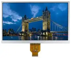
MCT101D12S1024600LML
TFT LCD, Transmissive, 10.1
⚠️ Reference pricing provided. In case of supply shortages, we will connect you with our trusted procurement partners to ensure your project's continuity.
- Manufacturer: MIDAS
- Product type: TFT LCD Displays
- VGA Size: WSVGA
- Resolution: 1024 x 600 Pixels
- Module Size: 235mm x 143mm
- Touchscreen: No Touchscreen
- Display Size: 10.1"
- Logic Voltage: 3.3V
- Display Pinout: 40 Way Connector
- Interface Type: LVDS
- Display Appearance: RGB
- Display Brightness: 160cd/m²
- Display Orientation: Landscape
- Operating Temperature Max: 60°C
- Operating Temperature Min: -10°C
| Delivery and price | |
|---|---|
| Units per pack | 1 |
| Price | 6.53 € |
| Current stock | 10+ |
| Lead time | 30 days |
Datasheet

+44 (0)1493 602602 +44 (0)1493 665111 sales@midasdisplays.com www.midasdisplays.com
**Midas Components Limited Telephone** Electra House **Fax** 32 Southtown Road **Email** Great Yarmouth **Website** Norfolk NR31 0DU England
**==> picture [318 x 379] intentionally omitted <==**
**----- Start of picture text -----**<br>
Specification<br>Part Number:<br>i metio1p12s1024600LmL<br>Version:<br>ee<br>Date:<br>2016/04/06<br>Revision<br>VERSION DATE REVISED PAGE NO. Note<br>0 2015/06/29 First issue<br>A 2016/01/21 Modify Static<br>electricity test<br>ee Key Attributes 2S... S..S........ i Display Accessories<br>TFT LCD MCIB-1<br>í{ëD!<br>Landscape<br>RGB<br>3.3V<br>[ë5{ Interface<br>cd/m2<br>X mm<br>- O~+ O degC<br>40 Way<br>**----- End of picture text -----**<br>
## Contents
1.Module Classification Information
2.Summary
- 3.General Specification
4.Interface
- 5.Contour Drawing
6.Absolute Maximum Ratings
- 7.Electrical Characteristics
- 8.Interface Timing Characteristics
- 9.Optical Characteristics
10.Reliability
11.Other
# **Midas Active Matrix Display Part Number System**
**MC T 057 A 6 * W 320240 L M L * *** 1 2 3 4 5 6 7 8 9 10 11 12 13
- 1 = MC: Midas Components
- 2
- =
- T: TFT A: Active Matrix OLED M: Monitor
- 3 =
- Size
- 4 =
- Series
- 5 = Viewing Angle: 6: 6 O’clock 12: 12 O’clock O: All Round Viewing Angle
- 6
- =
- Blank: No Touch T: Resistive Touchscreen C: Capacitive Touchscreen
- 7 = Operating Temp Range: S: 0+50Deg C B: -20+60Deg C W: -20+70Deg C E: -30+85Deg C X: -30+80Deg C
- 8
- =
- No of Pixels
- 9 =
- Orientation: P: Portrait L: Landscape
- Mode: R: Reflective M: Transmissive T: Transflective
- 10 = M: Transmissive T: S: Sunlight Readable (Transmissive) W: White on Black (Monochrome)
- Backlight: Blank: None L: LED C: CCFL
- 11 = Backlight: None L: LED C: CCFL 12 = Blank: No Module/board C: Controller board module (E-Tech)
- 12 = C: 13 = Blank: None OB: Optically Bonded IPS: In‐plane switching
## **3.General Specifications**
- Size: 10.1 inch
- Dot Matrix: 1024 RGB X 600 dots
- Module dimension: 235(W) x143(H) x 3.0(D) mm
- Active area: 222.72 (H) x 125.28(V) mm
- Dot pitch: 0.2175(W) x 0.2088(H) mm
- LCD type: TFT, Normally White, Transmissive
- View Direction: 12 o’clock
- Gray Scale Inversion Direction: 6 o’clock
- Backlight Type: LED,Normally White
- With /Without TP: Without TP
- Surface: Anti-Glare
*Color tone slight changed by temperature and driving voltage.
## **4.Interface**
## **4.1. TFT LCD MODULE**
|**PinNo.**|**Symbol**|**Description**|
|---|---|---|
|1|VCOM|Common voltage|
|2|VDD|Digitalpower|
|3|VDD|Digitalpower|
|4|NC|Not connect|
|5|RESET|Global reset pin. Active low to enter reset state. Suggest to<br>connecting with an RC reset circuit for stability. Normally pull high.<br>(R=10KΩ,C=1μF)|
|6|STBYB|Standby mode, normally pull high STBYB=”1”, normal operation<br>STBYB=”0”,timing control, source driver will turn off, all output are<br>high-Z|
|7|GND|Digitalground|
|8|NIND0|Negative LVDS differential data inputs|
|9|PIND0|Positive LVDS differential data inputs|
|10|GND|Digitalground|
|11|NIND1|Negative LVDS differential data inputs|
|12|PIND1|Positive LVDS differential data inputs|
|13|GND|Digitalground|
|14|NIND2|Negative LVDS differential data inputs|
|15|PIND2|Positive LVDS differential data inputs|
|16|GND|Digitalground|
|17|NINC|Negative LVDS differential clock inputs|
|18|PINC|Positive LVDS differential clock inputs|
|19|GND|Digitalground|
|20|NIND3|Negative LVDS differential data inputs|
|21|PIND3|Positive LVDS differential data inputs|
|22|GND|Digitalground|
|23|NC|Not connect|
|24|NC|Not connect|
|25|GND|Digitalground|
|26|NC|Not connect|
|27|NC|Not connect|
|28|SELB|6-bit/8-bit input select SELB = L , 8-bit ; SELB = H , 6-bit|
|29|AVDD|Analog power|
|30|GND|Digitalground|
|31|VLED-|LED Cathode|
|32|VLED-|LED Cathode|
|33|SHLR|Left or right displaycontrol|
|34|UPDN|Up/ down displaycontrol|
|35|VGL|Negativepower for TFT|
|36|NC|Not connect|
|37|NC|Not connect|
|---|---|---|
|38|VGH|Positivepower for TFT|
|39|VLED+|LED Anode|
|40|VLED+|LED Anode|
## **5.Contour Drawing**
**==> picture [456 x 280] intentionally omitted <==**
**----- Start of picture text -----**<br>
235.00¡ Ó0.3<br>226.00 5.35<br>1 VCOM 21 RXin3+<br>222.72(AA) 6.94<br>2 VDD 22 GND<br>116.70 3.00¡ Ó0.2 3 VDD 23 NC<br>4 NC 24 NC<br>5 Reset 25 GND<br>6 STBYB 26 NC<br>7 GND 27 NC<br>8 RXin0- 28 SELB<br>9 RXin0+ 29 AVDD<br>10 GND 30 GND<br>11 RXin1- 31 LED-<br>12 RXin1+ 32 LED-<br>13 GND 33 L/R<br>14 RXin2- 34 U/D<br>15 RXin2+ 35 VGL<br>16 GND 36 NC<br>17 RXCLKN- 37 NC<br>18 RXCLKN+ 38 VGH<br>19 GND 39 LED+<br>20 RXin3- 40 LED+<br>Component AreaH MAX:1.2mm<br>35.86<br>1 40<br>P0.5*39=19.50¡ Ó0.05 0.30¡ Ó0.05<br>106.45¡ Ó0.8 20.50<br>The non-specified tolerance of dimension is 0.3mm.<br>4.15 5.76<br>68.40<br> Ó0.3¡<br>128.50<br>143.00 125.28(AA)<br> Ó0.8¡<br>45.30 3.50<br>**----- End of picture text -----**<br>
**==> picture [286 x 155] intentionally omitted <==**
**==> picture [56 x 44] intentionally omitted <==**
**----- Start of picture text -----**<br>
A K<br>40 1<br>5.00¡ Ó0.2<br>**----- End of picture text -----**<br>
**==> picture [207 x 9] intentionally omitted <==**
**----- Start of picture text -----**<br>
The non-specified tolerance of dimension is 0.3mm.<br>**----- End of picture text -----**<br>
## **6.Absolute Maximum Ratings**
|**Item**|**Symbol**|**Min**|**Typ**|**Max**|**Unit**|
|---|---|---|---|---|---|
|Operating Temperature|TOP|-10|-|+60|�|
|Storage Temperature|TST|-20|-|+70|�|
Note: Device is subject to be damaged permanently if stresses beyond those absolute maximum ratings listed above
1. Temp. ≦60 � , 90% RH MAX. Temp. > 60 � , Absolute humidity shall be less than 90% RH at 60 �
**==> picture [148 x 130] intentionally omitted <==**
**----- Start of picture text -----**<br>
Ambient Tem. vs Alloeable Forward Curren<br>40<br>30<br>20<br>10<br>00 20 40 60 80 100<br>Ambient Temperature(oC)<br>Alloeable Forward Current IF(mA)<br>**----- End of picture text -----**<br>
## **7.Electrical Characteristics**
## **° 7.1. Typical Operation Conditions (At Ta = 25 C,)**
|<br>**ITEM**|<br>**SYMBOL**|**MIN**|**TYP**|**MAX**|**UNIT**|**NOTE**|
|---|---|---|---|---|---|---|
|Digital Power Supply Voltage For<br>LCD|VDD|3|3.3|3.6|V|-|
|Analog Power Supply Voltage|AVDD|--|10.4|11|V|-|
|Gate On Power Supply Voltage|VGH|20|21|22|V|-|
|Gate Off Power Supply Voltage|VGL|-8.5|-8|-7|V|-|
|Common Power Supply Voltage|VCOM|--|3.8|--|V|Note1|
|Logic Input Voltage|VIH|0.7*DVDD|-|DVDD|V|-|
||VIL|GND|-|0.3*DV<br>DD|V||
Note1.Please adjust VCOM to make the flicker level be minimum.
## **7.2. Backlight Driving Conditions**
|Parameter|Symbol|Min.|Typ.|Max.|Unit|Note|
|---|---|---|---|---|---|---|
|Supply voltage of white LED<br>backlight|VL|8.4|9.6|10.8|V|Note<br>1|
|Current for LED backlight|IL|135|140|150|mA||
|Uniformity|△|70|75|-|%||
|LED life time|-|20,000|-|-|Hr|Note2|
Note 1: The LED Supply Voltage is defined by the number of LED at Ta=25� and IL =140mA. Note 2: The “LEDlife time” is defined as the module brightness decrease to 50%original brightness at Ta=25� and IL =140mA. The LED lifetime could be decreased if operating IL is lager than 140mA.
## **8.Timing Characteristics DE mode**
|**DE mode**|||||||
|---|---|---|---|---|---|---|
|**Item**|**Symbol**||**Values**||**Unit**|**Remark**|
|||**Min.**|**Typ.**|**Max.**|||
|Horizontal Display Area|thd|-|1024|-|DCLK||
|DCLK Frequency|fclk|40.8|51.2|67.2|MHz||
|One Horizontal Line|th|1114|1344|1400|DCLK||
|HS Blanking|Thb+thfp|<br>90|320|376|DCLK||
|Vertical display area|tvd|-|600|-|H||
|VSYNC period time|tv|610|635|800|H||
|VSYNC blanking|tvb+tvfp|10|85|200|H||
|**9.Optical Characteristics**|**9.Optical Characteristics**|**9.Optical Characteristics**|**9.Optical Characteristics**||||||
|---|---|---|---|---|---|---|---|---|
|Item||Symbol|Condition.|Min|Typ.|Max.|Unit|Remark|
|Response time||Tr|θ=0°、Φ=0°|<br>-<br>-|4|-|.ms|Note 3|
|||Tf|||4|-|.ms|Note 3|
|Contrast ratio||CR|At optimized<br>viewing angl|<br>e<br>-|600|-|-|Note 4|
|Color Chromaticity|White|Wx|θ=0°、Φ=0|<br>0.24<br>0.28|5<br>0.295|0.345|-|Note 2,5|
|||Wy|||1<br>0.331|0.381|-||
|Viewing angle<br>(Gray Scale Inversion<br>Direction)|Hor.|ΘR|CR≧10|-<br>-<br>-<br>-|65|-|Deg.|Note 1|
|||ΘL|||65|-|||
||Ver.|ΦT|||55|-|||
|||ΦB|||65|-|||
|Brightness||-|-|140|<br>160|-|cd/m 2|Center of<br>display|
Ta=25±2 �
Note 1: Definition of viewing angle range
**==> picture [135 x 64] intentionally omitted <==**
Fig. 9.1. Definition of viewing angle
Note 2: Test equipment setup:
After stabilizing and leaving the panel alone at a driven temperature for 10 minutes, the measurement should be executed. Measurement should be executed in a stable, windless, and dark room. Optical specifications are measured by Topcon BM-7 or BM-5 luminance meter 1.0° field of view at a distance of 50cm and normal direction.
**==> picture [86 x 52] intentionally omitted <==**
**==> picture [211 x 11] intentionally omitted <==**
**----- Start of picture text -----**<br>
Fig. 9.2. Optical measurement system setup<br>**----- End of picture text -----**<br>
Note 3: Definition of Response time:
The response time is defined as the LCD optical switching time interval between “White” state and “Black” state. Rise time, Tr, is the time between photo detector output intensity changed from 90%to 10%. And fall time, Tf, is the time between photo detector output intensity changed from 10%to 90%
**==> picture [386 x 99] intentionally omitted <==**
**----- Start of picture text -----**<br>
D is p la y<br>D a ta W h ite (T F T O F F ) B la c k (T F T O N ) W h ite (T F T O F F )<br>1 0 0 %<br>9 0 %<br>1 0 %<br>0 %<br>**----- End of picture text -----**<br>
Note 4: Definition of contrast ratio:
The contrast ratio is defined as the following expression.
Luminance measured when LCD on the "White" state Contrast ratio (CR) = Luminance measured when LCD on the "Black" state
Note 5: White Vi = Vi50 ± 1.5V Black Vi = Vi50 ± 2.0V “±” means that the analog input signal swings in phase with VCOM signal. “±” means that the analog input signal swings out of phase with VCOM signal. The 100% transmission is defined as the transmission of LCD panel when all the input terminals of module are electrically opened.
Note 6: Definition of color chromaticity (CIE 1931) Color coordinates measured at the center point of LCD
Note 7: Measured at the center area of the panel when all the input terminals of LCD panel are electrically opened.
Updated at February 9, 2023
About Novapart
Novapart is a B2B electronic component broker specialising in stock shortages and cost reduction. We source hard-to-find parts and identify compliant alternatives across a catalogue of 410,000+ components from 500+ manufacturers.
Learn more →Stock Shortage Specialist
When a component is unavailable, discontinued or has an unacceptable lead time, we tap into our network of vetted European and Asian distributors to source what you need — without compromising on quality or traceability.
Request a quote →Compliant Alternatives
We identify pin-to-pin, electrically equivalent substitutes that meet the same certifications (RoHS, AEC-Q100, REACH) as your original specification — validated against datasheets, not just part numbers. Often at a lower cost.
BOM Analysis service →