
Image not available
Illustrative purposes only

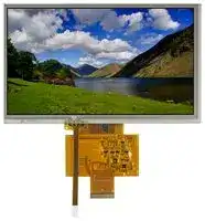
MCT070Z0CW1W800480LML
TFT LCD, Transmissive, 7
⚠️ Reference pricing provided. In case of supply shortages, we will connect you with our trusted procurement partners to ensure your project's continuity.
- Manufacturer: MIDAS
- Product type: TFT LCD Displays
- VGA Size: SVGA
- Resolution: 800 x 480 Pixels
- Module Size: 165mm x 100mm
- Touchscreen: Capacitive Touch
- Display Size: 7"
- Logic Voltage: 3.3V
- Product Range: Active Matrix OLED
- Display Pinout: 40 Way Connector
- Interface Type: RGB
- Display Appearance: RGB
- Display Brightness: 300cd/m²
- Display Orientation: Landscape
- Operating Temperature Max: 70°C
- Operating Temperature Min: -20°C
| Delivery and price | |
|---|---|
| Units per pack | 50 |
| Price | 66.31 € |
| Current stock | 10+ |
| Lead time | 30 days |
Datasheet

**Midas Components Limited Telephone** +44 (0)1493 602602 Electra House **Fax** +44 (0)1493 665111 32 Southtown Road **Email** sales@midasdisplays.com Great Yarmouth **Website** www.midasdisplays.com Norfolk NR31 0DU England ## **Specification** Part Number: ~~|~~ Version: Date: **==> picture [64 x 13] intentionally omitted <==** **----- Start of picture text -----**<br> Revision<br>**----- End of picture text -----**<br> 0 2016/05/26 First issue ## Contents - 1.Module Classification Information - 2.Summary - 3.General Specification - 4.Interface - 5.Contour Drawing - 6.Block Diagram - 7.Absolute Maximum Ratings - 8.Electrical Characteristics 9.DC Characteristics 10.AC Characteristics - 11.Optical Characteristics 12.Reliability 13.Touch Panel Information 14.Other # **Midas Active Matrix Display Part Number System** **MC T 057 A 6 * W 320240 L M L * *** 1 2 3 4 5 6 7 8 9 10 11 12 13 - 1 = MC: Midas Components - 2 - = - T: TFT A: Active Matrix OLED - 3 - = - Size - 4 = - Series - 5 = Viewing Angle: 6: 6 O’clock 12: 12 O’clock O: All Round Viewing Angle - 6 - = Blank: No Touch T: Resistive Touchscreen C: Capacitive Touchscreen - = Operating Temp Range: S: 0+50Deg C B: -20+60Deg C W: -20+70Deg C E: -30+85Deg C X: -30+80Deg C - 7 - No of Pixels - 8 - = = Orientation: P: Portrait L: Landscape - 9 = - 10 = Mode: R: Reflective M: Transmissive T: Transflective - S: Sunlight Readable (Transmissive) W: White on Black (Monochrome) - 11 = Backlight: Blank: None L: LED C: CCFL 12 = Blank: No Module/board C: Controller board module (E-Tech) - 12 = C: 13 = Blank: None OB: Optically Bonded IPS: In‐plane switching ## **2.Summary** This technical specification applies to 7.0’ color TFT-LCD panel. The 7.0’ color TFT-LCD panel is designed for camcorder, digital camera application and other electronic products which require high quality flat panel displays. This module follows RoHS. ## **3.General Specifications** - Size: 7.0 inch - Dot Matrix: 800 x RGBx480(TFT) dots - Module dimension: 165.0(W) x 100(H) x 7.475(D) mm - Active area: 154.08 x 85.92 mm - Dot pitch: 0.0642 x 0.179 mm - LCD type: TFT, Normally White, Transmissive - View Direction: 12 o’clock - Gray Scale Inversion Direction: 6 o’clock - CTP FW Version: 09 - Backlight Type: LED, Normally White - With /Without TP: With CTP - Surface: Glare *Color tone slight changed by temperature and driving voltage. ## **4.Interface** ## **4.1. LCM PIN Definition** |**4.1. LCM PIN Definition**|**4.1. LCM PIN Definition**||| |---|---|---|---| |**Pin**|**Symbol**|**Function**|**Remark**| |1|VLED-|Backlightground|| |2|VLED+|Power supplyfor backlight|| |3|GND|Powerground|| |4|VCC|Power for Digital Circuit|| |5|R0|Red data(LSB)|Note 1| |6|R1|Red data|Note 1| |7|R2|Red data|| |8|R3|Red data|| |9|R4|Red data|| |10|R5|Red data|| |11|R6|Red data|| |12|R7|Red data(MSB)|| |13|G0|Green data(LSB)|Note 1| |14|G1|Green data|Note 1| |15|G2|Green data|| |16|G3|Green data|| |17|G4|Green data|| |18|G5|Green data|| |19|G6|Green data|| |20|G7|Green data(MSB)|| |21|B0|Blue data(LSB)|Note 1| |22|B1|Blue data|Note 1| |23|B2|Blue data|| |24|B3|Blue data|| |25|B4|Blue data|| |26|B5|Blue data|| |27|B6|Blue data|| |28|B7|Blue data(MSB)|| |29|GND|Power Ground|| |30|CLK|Sample clock|Note 2| |31|R/L|Right /Left selection|Note 3,4| |32|Hsync|Horizontal Sync Input|| |33|Vsync|Vertical Sync Input|| |34|NC|No connection|| |35|U/D|Up/down selection|Note 3,4| |36|RESET|Global resetpin.|| |37|NC|No connection|| |38|NC|No connection|| |39|NC|No connection|| |40|NC|No connection|| Note 1: When input 18 bits RGB data, the two low bits of R,G and B data must be grounded. Note 2: Data shall be latched at the falling edge of CLK. Note 3: Selection of scanning mode Setting of scan control Scanning direction U/D R/L GND VCC Up to down, left to right VCC GND Down to up, right to left GND GND Up to down, right to left ~~=~~ VCC VCC ~~=~~ Down to up, left to right Note 4: Definition of scanning direction. Refer to the figure as below: **==> picture [168 x 94] intentionally omitted <==** **----- Start of picture text -----**<br> Up<br>Left Right<br>Down<br>**----- End of picture text -----**<br> Note 5: Global reset pin. Active low to enter reset state . Suggest to connect with an RC reset circuit for stability. Normally pull high. Note 6: Dithering function enable control, normally pull high. When DITHB=”1”, Disable internal dithering function, When DITHB=”0”, Enable internal dithering function, ## **4.2. CTP PIN Definition** |**Pin**|**Symbol**|**Function**|**Remark**| |---|---|---|---| |1|**Symbol**<br>VSS|Ground for analog circuit|| |2|VDDT|Power Supply: +3.0V|| |3|SCL|I2C clock input|| |4|NC|No connect|| |5|SDA|I2C datainputand output|| |6|NC|No connect|| |7|/RST|External Reset, Low is active|| |8|/WAKE|External interrupt from the host|| |9|/INT|External interrupt to the host|| |10|VSS|Ground for analogcircuit|| ## **5.Contour Drawing** **==> picture [209 x 343] intentionally omitted <==** **----- Start of picture text -----**<br> 1 VLED-<br>2 VLED+<br>3 GND<br>4 VCC<br>5 R0<br>6 R1<br>7 R2<br>8 R3<br>9 R4<br>10 R5<br>11 R6<br>12 R7<br>13 G0<br>14 G1<br>15 G2<br>16 G3<br>17 G4<br>18 G5<br>19 G6<br>20 G7<br>21 B0<br>22 B1<br>23 B2<br>24 B3<br>25 B4<br>: 32 : 2267 B6B5<br>hizo 28 B7<br>29 GND<br>! | 30 CLK<br>31 R/L<br>d 32 Hsync<br>33 Vsync<br>34 NC<br>35 U/D<br>i 401926 = 2 3637 RESETNC<br>38 NC<br>39 NC<br>1 40 NC<br>The non-specified tolerance of dimension is 0.3mm.<br>* =<br>**----- End of picture text -----**<br> ## **6.Block Diagram** **==> picture [455 x 217] intentionally omitted <==** **----- Start of picture text -----**<br> CLK<br>| [a] [l] TIMING<br>R0~R7 = CONTROLLER L m TFT LCD<br>G0~G7 ~ _ PANEL<br>B0~B7 ~ ~<br>Vsync,Hsync<br>| [a]<br>RESET =<br>|al<br>VCC = = DATA DRIVER IC<br>R/L,U/D | ae<br>GND =<br>VLED+<br>= LED CONNECTOR = BACKLIGHT UNIT<br>VLED-<br>I2C I2C<br>CTP Signal — an — _ CTP<br>Capacitive Touch Panel Signal<br>SCAN DRIVER IC<br>INPUT CONNECTOR<br>**----- End of picture text -----**<br> ## **7.Absolute Maximum Ratings** |**Item**|**Symbol**<br>~~ee~~|**Min**<br>~~ee~~|**Typ**<br>~~ee~~|**Max**|**Unit**| |---|---|---|---|---|---| |Operating Temperature<br>~~es~~|TOP<br>~~es~~<br>~~ee~~<br>~~ee~~|-20<br>~~es~~<br>~~ee~~<br>~~ee~~|-<br>~~es~~<br>~~ee~~<br>~~ee~~|+70<br>~~es~~|~~es~~| |Storage Temperature<br>~~rr~~|TST<br>~~ee ~~<br>~~rr~~<br>~~ee~~|-30<br> ~~ee~~<br>~~rr~~<br>~~ee~~|-<br>~~ee~~<br>~~rr~~<br>~~ee~~|+80<br>~~rr~~|~~rr~~| **==> picture [228 x 159] intentionally omitted <==** **----- Start of picture text -----**<br> 1. Temp. L160), 90% RH MAX. Temp. ><br>at 60/1<br>Ambient Tem. vs Alloeable Forward Curren<br>40<br>30<br>20<br>10<br>00 20 40 60 80 100<br>Ambient Temperature(oC)<br>Alloeable Forward Current IF(mA)<br>**----- End of picture text -----**<br> ## **8.Electrical Characteristics** ## **8.1. Operating conditions:** |**8.1. Operating conditions:perating conditions:erating conditions:g conditions: conditions:**||||||| |---|---|---|---|---|---|---| |**Item**|**Symbol**|**Min**|**Typ**|**Max**|**Unit**|Remark| |Supply Voltage For Logic|VCC|3.0|3.3|3.6|V|Note 1| |Power Supply For Current|VCC =3.3V||110|165|mA|| |Supply Voltage For Touch<br>Logic|Supply Voltage For Touch<br>VDDT|2.8|-|3.3|V|| Note 1 : This value is test for Vcc=3.3V , Ta=25 ℃ only ## **8.2. LED driving conditions** |**8.2. LED driving conditionsg conditions conditions**||||||| |---|---|---|---|---|---|---| |Parameter|Symbol|Min.|Typ.|Max.|Unit|Remark| |LEDcurrent|-|-|180|-|mA|-| |PowerConsumption|-|1620|-|1890|mW|-| |LED voltage|A~K|9.0|-|10.5|V|Note1| |LED Life Time|-|-|50,000|-|Hr|Note<br>2,3,4| Note 1 : There are 1 Groups LED Note 2 : Ta = 25 ℃ Note 3 : Brightness to be decreased to 50% of the initial value Note 4 : The single LED lamp case ## **9.DC CHARATERISTICS** |**Parameter**|**Symbol**|**Rating**|**Rating**|**Rating**|**Unit**|**Condition**| |---|---|---|---|---|---|---| |||**Min**|**Typ**|**Max**||| |Low level input voltage|VIL|0|-|0.3VCC|V|| |High level input voltage|High level input voltage<br>VIH|0.7VCC|-|VCC|V|| ## **10.AC CHARATERISTICS** ## **10.1. AC Electrical Characteristics** |**Signal**|**Symbol**|**Min**|**Typ**|**Max**|**Unit**| |---|---|---|---|---|---| |HS setuptime|Thst|8|-|-|ns| |HS hold time|Thhd|8|-|-|ns| |VS setuptime|Tvst|8|-|-|ns| |VS hold time|Tvhd|8|-|-|ns| |Data setuptime|Tdsu|8|-|-|ns| |Data hole time|Tdhd|8|-|-|ns| |VCC Power On Slew rate|TPOR|-|-|20|ms| |RESETpulse width|TRst|1|-|-|ms| |DCLK cycle time|Tcoh|20|-|-|ns| |DCLKpulse duty|Tcwh|40|50|60|%| ## **10.2. Input Clock and Data Timing Diagram** ## **10.3. Timing** |**10.3. Timingg **||||||| |---|---|---|---|---|---|---| |**Item**|**Symbol**|**Values**|||**Unit**|**Remark**| |||**Min.**|**Typ.**|**Max.**||| |CLK Frequency (DCLK)|fclk|26.4|33.3|46.8|MHz|| |Horizontal DisplayArea|thd|-|800|-|CLK|| |One Horizontal Line|th|862|1056|1200|CLK|| |HSpulse width|thpw|1|-|40|CLK|| |HS Blanking|thb|46|46|46|CLK|| |HS Front Porch|thfp|16|210|354|CLK|| |Vertical DisplayArea|tvd|-|480|-|TH|| |VSperiod time|tv|510|525|650|TH|| |VSpulse width|tvpw|1|-|20|TH|| |VS Blanking|tvb|23|23|23|TH|| |VS Front Porch|tvfp|7|22|147|TH|| ## **10.4. Data Input Format** Fig. Horizontal input timing diagram Fig. Vertical input timing diagram ## **11.Optical Characteristics** ~~pO~~ **Item Symbol Condition. Min Typ. Max. Unit Remark** Tr - 10 20 .ms Response time θ=0° 、 Φ=0° Note 3 ~~ee~~ Tf - 15 30 .ms At optimized Contrast ratio CR viewing 400 500 - - Note 4 angle Wx 0.26 0.30 0.32 - Note ~~rr~~ Color Chromaticity White θ=0° ~~eee~~ 、 Φ=0 ~~ee~~ Wy 0.27 0.28 0.33 - 2,5,6 ΘR - 75 - Viewing angle Hor. ΘL - 75 - (Gray Scale Inversion ~~| ||~~ CR ≧ 10 ~~esa eeee ee~~ Deg. ee Note 1 ΦT - 75 - Direction) Ver. ~~| |} —~~ ΦB ~~**a**~~ - ~~ee~~ 75 - Brightness - - 200 300 - cd/m[2][Center of ] ~~OO~~ display Ta=25±2 ℃ , IL=180mA Note 1: Definition of viewing angle range Fig. 11.1. Definition of viewing angle Note 2: Test equipment setup: After stabilizing and leaving the panel alone at a driven temperature for 10 minutes, the measurement should be executed. Measurement should be executed in a stable, windless, and dark room. Optical specifications are measured by Topcon BM-7orBM-5 luminance meter 1.0° field of view at a distance of 50cm and normal direction. Fig. 11.2. Optical measurement system setup Note 3: Definition of Response time: The response time is defined as the LCD optical switching time interval between “White” state and “Black” state. Rise time, Tr, is the time between photo detector output intensity changed from 90%to 10%. And fall time, Tf, is the time between photo detector output intensity changed from 10%to 90% **==> picture [377 x 81] intentionally omitted <==** **----- Start of picture text -----**<br> D is p la y<br>D a ta W h ite (T F T O F F ) B la c k (T F T O N ) W h ite (T F T O F F )<br>w<br>1 0 0 %<br>9 0 %<br>Q=<br>3<br>Ss<br>1 0 %<br>= 0 %<br>**----- End of picture text -----**<br> Note 4: Definition of contrast ratio: The contrast ratio is defined as the following expression. Lum inance m easured when LCD on the "W hite" state Contrast ratio (CR) = Lum inance m easured when LCD on the "Black" state Note 5: White Vi = Vi50 ± 1.5V Black Vi = Vi50 ± 2.0V “±” means that the analog input signal swings in phase with VCOM signal. “±” means that the analog input signal swings out of phase with VCOM signal. The 100% transmission is defined as the transmission of LCD panel when all the input terminals of module are electrically opened. Note 6: Definition of color chromaticity (CIE 1931) Color coordinates measured at the center point of LCD Note 7: Measured at the center area of the panel when all the input terminals of LCD panel are electrically opened. ## **12.Reliability** **Environmental Test** **==> picture [472 x 379] intentionally omitted <==** **----- Start of picture text -----**<br> |||||||| |---|---|---|---|---|---|---| |DG|Test Item|Content|of Test|Test|Condition|Note| |High Temperature|Endurance test applying the high storage temperature|2| |a|storage|ee|for a long time.|200hrs| |Low Temperature|Endurance test applying the low storage temperature|1,2| |a|storage|for a long time.|200hrs|ee| |High Temperature|Endurance test applying the electric stress (Voltage &|——| |Operation|Current) and the thermal stress to the element for a|200hrs| |long time.| |Low Temperature|Endurance test applying the electric stress under low|1| |a|Operation|ee|temperature for a long time.|200hrs| |High Temperature/|The module should be allowed to stand at|1,2| |Humidity|Operation|6001,90%RH|max|96hrs| |Thermal shock|The sample should be allowed stand the following 10|-20/700|——| |resistance|cycles of|10 cycles| |operation| |-200)|250|700| |30min 5min 30min| |1 cycle| |Vibration test|Endurance test applying the vibration during|Total fixed amplitude : 3| |transportation and using.|15mm| |Vibration Frequency :| |10~55Hz| |One cycle 60| |seconds to 3| |directions of X,Y,Z for| |Each 15 minutes| |Static electricity test|Endurance test applying the electric stress to the|VS=±600V(contact)|——| |terminal.|,±800v(air),| |RS=330Ω| |CS=150pF| |10 times| **----- End of picture text -----**<br> Note1: No dew condensation to be observed. Note2: The function test shall be conducted after 4 hours storage at the normal Temperature and humidity after remove from the test chamber. Note3: The packing have to including into the vibration testing. ## **13.Touch Panel Information** **==> picture [438 x 163] intentionally omitted <==** **----- Start of picture text -----**<br> ¡ ° Sensor OD<br>—<br>\ ii ! i<br>0,0 0x1c<br>0x10 0x18 ¢<br>Slide<br>¡ G<br>0x14<br>\ | N ty 7<br>2 i i TT<br>¥ ¿ ±Â ж ¦ â? º Ï« ̽ ª½ ¤<br> ? §é? °ì a<br>yal Cec i -- Ty<br>° Sensor OD<br>¡<br>**----- End of picture text -----**<br> ## **13.1. CTP I2C Timing:** I2C Serial Data Transfer Format I2C master write, slave read ||I2C master read,slave write| |---|---| |**Mnemonics**|**Description**| |S|12C Start or 12C Restart| |A[6:0]|Slave address| |R/W|READ/WRITE bit,‘1' for read,‘0' for write| |A(N)|ACK(NACK)bit| |P|STOP :the indication of the end of a packet(if this bit is missing, S will<br>indicate the end of the currentpacket and beginningof the nextpacket)| Lists the meanings of the mnemonics used in the above figures |**Parameter**|**Unit**|**Min**|**Max**| |---|---|---|---| |SCL frequency|KHz|0|400| |Bus free time between a STOP and START condition|us|4.7|\| |Hold time(repeated)ST ART condition|us|4.0|\| |Data setuptime|ns|250|\| |Setuptime for a repeated START condition|us|4.7|\| |Setuptime for STOP condition|us|4.0|\| Interface Timing Characteristics AS FOR STANDARD CTPM, HOST NEED TO USE BOTH INTERRUPT CONTROL SIGNAL AND SERIAL DATA INTERFACE TO GET THE TOUCH DATA. HERE IS THE TIMING TO GET TOUCH DATA. ## **13.2. WRITE BYTES TO I2C SLAVE** AS FOR STANDARD CTPM, HOST NEED TO USE BOTH INTERRUPT CONTROL SIGNAL AND SERIAL DATA INTERFACE TO GET THE TOUCH DATA, HERE IS THE TIMING TO GET TOUCH DATA. ## Address: 0X38 ## TOUCH DATA READ PROTOCOL |**NAME**|**VALUE**|**DESCRIPTION**| |---|---|---| |START CH|0X00|START COMMAND FOR CTPM TOUCH DATA<br>PACKET,HOST MUST SEND CTPM A START CH<br>COMMAND BEFORE READ TOUCH DATA| |lst READ BYTE~<br>LAST READ BYTE||TOUCH DATA PACKET<br>SENT BY CTPM,EACH BYTE HAS 8-BIT DATA ,A<br>TOUCH DATA<br>PACKET CONSISTS OF N BYTE| A DATA PACKET STARTS WITH A HEADER AND ENDS WITH CRC CODE,AS FOR 5 POINTS DATA PACKET,THE LENGTH OF THE PACKET IS ALWAYS 26 BYTES IN SPITE OF ACTUAL TOUCH POINTS. |**Address**|**Name**|**Bit7 Bit6**|**Bit7 Bit6**|**Bit5**|**Bit4**|**Bit3**|**Bit2**|**Bit1 Bit0**|**Bit1 Bit0**|**Bit1 Bit0**|**Host**<br>**Access**| |---|---|---|---|---|---|---|---|---|---|---|---| |00h|Devide_Mode||Device Model[2:0]|||||||RW|| |01h|Gest_ID|Gesture ID[7:0]||||||||R|| |02h|TD_Status|||||Number of<br>touchpoints[3:0]||||R|| |03h|Touch1_XH|1st Event<br>Flag||||1stTouch<br>X Position[11:8]||||R|| |04h|Touch1_XL|1stTouch X Position[7:0]||||||||R|| |05h|Touch1_YH|1st Touch ID[3:0]||||1st Touch<br>Y Position[11:8]||||R|| |06h|Touch1_YL|1st Touch Y Position[7:0]||||||||R|| |09h|Touch2_XH|2ndEvent<br>Flag||||2ndTouch<br>X Position[11:8]||||R|| |0Ah|Touch2_XL|2nd Touch X Position[7:0]||||||||R|| |0Bh|Touch2_YH|2nd Touch ID[3:0]|2nd Touch ID[3:0]|2ndTouch<br>Y Position[11:8]|R| |---|---|---|---|---|---| |0Ch|Touch2_YL|2nd Touch Y Position[7:0]|||R| |0Fh|Touch3_XH|3rdEvent<br>Flag||3rdTouch<br>X Position[11:8]|R| |10h|Touch3_XL|3rd Touch X Position[7:0]|||R| |11h|Touch3_YH|3rdTouch ID[3:0]||3rdTouch<br>Y Position[11:8]|R| |12h|Touch3_YL|3rd Touch Y Position[7:0]|||R| |15h|Touch4_XH|4thEvent<br>Flag||4thTouch<br>X Position[11:8]|R| |16h|Touch4_XL|4th Touch X Position[7:0]|||R| |17h|Touch4_YH|4thTouch ID[3:0]||4thTouch<br>Y Position[11:8]|R| |18h|Touch4_YL|4th Touch Y Position[7:0]|||R| |1Bh|Touch5_XH|5thEvent<br>Flag||5thTouch<br>X Position[11:8]|R| |1Ch|Touch5_XL|5th Touch X Position[7:0]|||R| |1Dh|Touch5_YH|5thTouch ID[3:0]||5thTouch<br>Y Position[11:8]|R| |1Eh|Touch5_YL|5th Touch Y Position[7:0]|||R|
Updated at February 9, 2023
About Novapart
Novapart is a B2B electronic component broker specialising in stock shortages and cost reduction. We source hard-to-find parts and identify compliant alternatives across a catalogue of 410,000+ components from 500+ manufacturers.
Learn more →Stock Shortage Specialist
When a component is unavailable, discontinued or has an unacceptable lead time, we tap into our network of vetted European and Asian distributors to source what you need — without compromising on quality or traceability.
Request a quote →Compliant Alternatives
We identify pin-to-pin, electrically equivalent substitutes that meet the same certifications (RoHS, AEC-Q100, REACH) as your original specification — validated against datasheets, not just part numbers. Often at a lower cost.
BOM Analysis service →