
Image not available
Illustrative purposes only

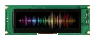
MCT052A6W480128LMLC
TFT LCD, 5.2
⚠️ Reference pricing provided. In case of supply shortages, we will connect you with our trusted procurement partners to ensure your project's continuity.
- Manufacturer: MIDAS
- Product type: TFT LCD Displays
- Resolution: 480 x 128 Pixels
- Module Size: 180mm x 65mm
- Touchscreen: No Touchscreen
- Display Size: 5.2"
- Logic Voltage: 3.3V
- Display Pinout: 36 Way FPC
- Interface Type: Parallel
- Display Appearance: RGB
- Display Brightness: 500cd/m²
- Display Orientation: Landscape
- Operating Temperature Max: 70°C
- Operating Temperature Min: -20°C
| Delivery and price | |
|---|---|
| Units per pack | 1 |
| Price | 35.02 € |
| Current stock | 10+ |
| Lead time | 30 days |
Datasheet

**Midas Components Limited Telephone** +44 (0)1493 602602 Electra House **Fax** +44 (0)1493 665111 32 Southtown Road **Email** sales@midasdisplays.com Great Yarmouth **Website** www.midasdisplays.com Norfolk NR31 0DU England
**Specification** Part Number: ~~|| MCT052A6W480128LMLC~~ Version: ~~ee~~ Date: **Revision VERSION DATE REVISED PAGE NO. Note** 0 2016/06/23 First issue
## Contents
- 1.Module Classification Information
2.Summary
- 3.General Specification
- 4.Interface
- 5.Contour Drawing
- 6.Block Diagram
- 7.Absolute Maximum Ratings 8.Electrical Characteristics
9.DC Characteristics
10.Interface Timing Characteristics
- 11.Optical Characteristics
12.Reliability
- 13.Display start address setting
14.Other
# **Midas Active Matrix Display Part Number System**
**MC T 057 A 6 * W 320240 L M L * *** 1 2 3 4 5 6 7 8 9 10 11 12 13
- 1 = MC: Midas Components
- 2
- =
- T: TFT A: Active Matrix OLED M: Monitor
- 3
- =
- Size
- 4 =
- Series
- 5 = Viewing Angle: 6: 6 O’clock 12: 12 O’clock O: All Round Viewing Angle
- 6
- = Blank: No Touch T: Resistive Touchscreen C: Capacitive Touchscreen
- 7 = Operating Temp Range: S: 0+50Deg C B: -20+60Deg C W: -20+70Deg C E: -30+85Deg C X: -30+80Deg C
- No of Pixels
- 8
- = = Orientation: P: Portrait L: Landscape
- 9 =
- 10 =
- Mode: R: Reflective M: Transmissive T: Transflective
- S: Sunlight Readable (Transmissive) W: White on Black (Monochrome)
- Backlight: Blank: None L: LED C: CCFL
- 11 = Backlight: None L: LED C: CCFL 12 = Blank: No Module/board C: Controller board module (E-Tech)
- 12 = C: 13 = Blank: None OB: Optically Bonded IPS: In‐plane switching
## **2.Summary**
This technical specification applies to 5.2’ color TFT-LCD panel. The 5.2’ color TFT-LCD panel is designed for camcorder, digital camera application and other electronic products which require high quality flat panel displays. This module follows RoHS.
## **3.General Specifications**
- Size: 5.2 inch
- Dot Matrix: 480 x RGBx128 dots
- Module dimension: 180.0 x 65.0 x 8.8 mm
- Active area: 127.152 x 33.9072 mm
- Dot pitch: 0.0883 x 0.2649 mm
- LCD type: TFT, Normally White, Transmissive
- View Direction: 6o’clock
- Gray Scale Inversion Direction: 12 o’clock
- Backlight Type: LED,Normally White
- Driver IC: SSD1963
- Interface: Digital 8080 family MPU 8bit/16bit
- With /Without TP: Without TP
- Surface: Glare
*Color tone slight changed by temperature and driving voltage.
## **4.Interface 4.1. LCM PIN Definition**
|**Pin**|**Symbol **|**Function **|**Remark**|
|---|---|---|---|
|1|GND|System round pin of the IC.<br>Connect to systemground.||
|2|VDD|PowerSupply:+3.3V||
|3|BL_E|Backlight controlsignal,H:On\L:Off||
|4|C/D|Data/Command select||
|5|WR|Write strobe signal||
|6|RD|Read strobe signal||
|7|DB0|Data bus||
|8|DB1|Data bus||
|9|DB2|Data bus||
|10|DB3|Data bus||
|11|DB4|Data bus||
|12|DB5|Data bus||
|13|DB6|Data bus||
|14|DB7|Data bus||
|15|DB8|Data bus (Whenselect 8bitsmode, this pin isNC)|Note1|
|16|DB9|Data bus (When select 8bits mode, this pin is NC)|Note1|
|17|DB10|Data bus (Whenselect 8bitsmode, this pin isNC)|Note1|
|18|DB11|Data bus (When select 8bits mode, this pin is NC)|Note1|
|19|DB12|Data bus (Whenselect 8bitsmode, this pin isNC)|Note1|
|20|DB13|Data bus (When select 8bits mode, this pin is NC)|Note1|
|21|DB14|Data bus (Whenselect 8bitsmode, this pin isNC)|Note1|
|22|DB15|Data bus (Whenselect 8bitsmode, this pin isNC)|Note1|
|23|NC|No connect||
|24|NC|No connect||
|25|CS|Chip select||
|26|RESET|Hardware reset||
|27|LR|Right /Left selection;DefaultR/L=High|Note2,3|
|28|UD|Up/downselection;Default U/D=High|Note2,3|
|29|NC|No connection||
|30|NC|No connection||
|31|NC|No connection||
|32|NC|No connection||
|33|VLED-|VLED- for B/L LED inverter(GND)||
|34|VLED-|VLED- for B/L LED inverter(GND)||
|35|VLED+|VLED+for B/L LED inverter(+5V)||
|36|VLED+|VLED+for B/L LED inverter(+5V)||
Note1: When select 8bit mode, DB0~DB7 be used, DB8~DB15 no connect When select 16bit mode, DB0~DB15 be used
Note 2: Selection of scanning mode
|Setting ofscancontrol input|Setting ofscancontrol input|Scanning direction|
|---|---|---|
|UD|LR||
|GND|VDD|Downto up,left toright|
|VDD|GND|Up to down,right toleft|
|GND|GND|Downto up,right toleft|
|VDD|VDD|Up to down,left toright|
Note 3: Definition of scanning direction.Refer to the figure as below:
**==> picture [74 x 24] intentionally omitted <==**
**----- Start of picture text -----**<br>
let 4<br>**----- End of picture text -----**<br>
## **4.2. LCM PIN Definition (CON1)**
|**Pin**|**Symbol **|**Function **|**Remark**|
|---|---|---|---|
|1|FG|Frame Grand||
|2|GND|System round pin of the IC.<br>Connect to systemground.||
|3|VDD|PowerSupply:+3.3V||
|4|BLE|Backlight controlsignal,H:On\L:Off||
|5|WR|Write strobe signal||
|6|RD|Read strobe signal||
|7|CS|Chip select||
|8|C/D|Data/Command select||
|9|NC|No connect||
|10|RESET|Hardwarereset||
|11|DB0|Data bus||
|12|DB1|Data bus||
|13|DB2|Data bus||
|14|DB3|Data bus||
|15|DB4|Data bus||
|16|DB5|Data bus||
|17|DB6|Data bus||
|18|DB7|Data bus||
|19|NC|No connect||
|20|NC|No connect||
|21|VLED+|VLED+for B/L LED inverter(+5V)|Note3|
|22|VLED-|VLED- for B/L LED inverter(GND)|Note3|
|23|NC|No connect||
|24|NC|No connect||
|25|NC|No connect||
|26|GND|Hardwarereset||
Note3:
When PCB right side CON1 select Pin1~Pin20, Pin21~Pin22 no connect, +5V can input on PCB left side VLED+/- PAD
## **5.Contour Drawing**
**==> picture [471 x 283] intentionally omitted <==**
**----- Start of picture text -----**<br>
2.0 176.0<br>19.2 141.70<br>23.5 133.0(VA) 8.80¡ Ó0.2<br>26.424 127.152(AA) 4.70<br>ee PE F 2.50<br>| B S Ko n L L!<br>; | | ee E H R<br>Gray Scale Inversion Direction | lL ie oo i<br>V LED+ x) i<br>eo i<br>V LED- | foXo} H<br>480xRGBx128 iit tape oo 4 EE |<br>y 4 SA GA E<br>1.50 40.00 (TFT FPC) 1.50 1.6<br>4-4- @ 3.5 PTH7.5PAD 43.00 68.50 5.50 =| te,<br>2 ©oO88 o¢ : 0.2649 0 .08 83<br>RGB<br>OO RGB<br>ge u l<br>20 " SC A L E 30:1<br>26- 1.0 PTH 4.13<br>26- 4@ 1.8 PAD 26 an ] PA 2.54<br>PIN DETAIL<br>SCALE 1/1<br>The non-specified tolerance of dimension is + 0.3mm.<br>5.5 9.3 15.56<br>0.50<br> Ó0.5¡ 54.0<br>65.0 51.17(FR) 39.0(VA) 33.907(AA)<br>13.0<br>0.2649<br>P2.54*12=30.48<br>**----- End of picture text -----**<br>
**==> picture [458 x 328] intentionally omitted <==**
**----- Start of picture text -----**<br>
1 FG 1 GND<br>2 GND 2 VDD<br>3 VDD 3 BL_E 99.74<br>a 4 BLE 4 C/D PO 34.50 25.00 61.00 25.00 34.50<br>5 WR 5 WR<br>| 6 | RD 6 RD ee<br>7 CS 7 DB0<br>8 C/D jf= 8 | DB1 fr o . oD BD P0.5*39 = 19.5 @ @w a -& 3.00 4A<br>f+} 10119 RESETDB0NC ee 10119 DB2DB3DB4 ee ee38 1 40 ene 1 a f VLED+ 5.00<br>12 DB1 12 DB5 VLED-<br>———— 1314 DB2DB3 1314 [| DB6DB7 rat 36 2-3.0PAD2-1.0PTH<br>15 DB4 15 DB8<br>ee 16 DB5 16 DB9 lem<br>17 DB6 17 DB10 40.00(TFT FPC)<br>18 DB7 — 18 DB11 34.50 25.00 is 61.00 25.00 34.50<br>19 NC 19 DB12<br>20 NC 20 DB13 31.4<br>ee 21 VLED+ 21 DB14 68.0 e 44.0<br>22 VLED- 22 DB15<br>23 NC 23 NC<br>eSr 24 NC f. 24 NC ee<br>25 NC 25 CS<br>eer 26 GND t.||jp [|] Lal 262728 || RESETUDLR<br>29 NC<br>|r, 30 NC The non-specified tolerance of dimension is + 0.3mm.<br>31 NC<br>\Fi™N 32 NC<br>=zit 333435 VLED+VLED-VLED- VaWw<br>36 VLED+<br>CON1 CON4<br>CON6<br>CN-FPC-36P/P0.5<br>(Down-Side)<br>15.5<br>29.00<br>7.00<br>35.90 34.00 (TP FPC hole)<br>32.5<br>CON1 CON4<br>**----- End of picture text -----**<br>
## **6.Block Diagram**
**==> picture [465 x 276] intentionally omitted <==**
**----- Start of picture text -----**<br>
Control board LCD Panel<br>TFT LCD VGH<br>UserConnector VDD supplybias Power VGH,VGL,AVDD,VCOM,POL supplyPower POLVGLAVDDVCOM<br>Power supply VDD,GND VDD VCC<br>SSD1963<br>Control D/C#C/S# LFRAME VS<br>Signal RD#(E) Registers LLINE HS<br>WR#(R/W) MCU<br>Interface LSHIFT PLCK<br>If 8 bit [7:0] Data Bus LDATA 〔 23 : 0 〕 RGB 24 Bit<br>If 16 bit [15:0]<br>LCD LDEN DE<br>Controller RESET RESET<br>Frame Buffer<br>5.2"<br>Reset RESET# and Reset MgrSystem Clock 480(RGB)x128<br>Rotation/<br>Mirror<br>Clock<br>Generator DBC<br>LR,UD LR,UD<br>Backlight Enable BLE H:ON Backlight ON/OFF<br>L:OFF<br>Backlight LED VLED+,VLED- Backlight Backlight LED Output LED +/- Backlight<br>IC Voltage IC Controller LED<br>LCD Interface<br>**----- End of picture text -----**<br>
**7.Absolute Maximum Ratings Item Symbol Min Typ Max Unit** Operating Temperature TOP -20 - +70 ℃ Storage Temperature TST -30 - +80 ℃ ~~=—aesree~~ Note: Device is subject to be damaged permanently if stresses beyond those absolute maximum ratings listed above
1. Temp. ≦ 60 ℃ , 90% RH MAX. Temp.>60 ℃ , Absolute humidity shall be less than 90% RH at 60 ℃
**==> picture [151 x 133] intentionally omitted <==**
**----- Start of picture text -----**<br>
Ambient Tem. vs Alloeable Forward Curren<br>40<br>30<br>20<br>10<br>00 20 40 60 80 100<br>Ambient Temperature(oC)<br>iM<br>Alloeable Forward Current IF(mA)<br>**----- End of picture text -----**<br>
## **8.Electrical Characteristics**
**8.1. Operating conditions: (CON3.Pin1=GND, Pin2=VDD)**
**Item Symbol Condition Min Typ Max Unit Remark** - - Supply Voltage For LCM VDD 3.0 3.1 3.3 V Supply Current For LCM IDD — — 200 — mA Note1 ~~a~~
Note 1 : This value is test for VDD =3.3V , Ta=25 ℃ only **8.2. Backlight driving conditions (CON3.Pin33,34=VLED-, Pin35,36=VLED+)** Parameter Symbol Min. Typ. Max. Unit Remark Operation Current For LED VLED=5V - 250 - mA Note 1,2 Driver Supply Voltage For LED Driver VLED+ - 5 - V Note 1,2 Note LED Life Time - 50,000 - Hr ~~po~~ 2,3,4 Note 1 : Base on VLED= 5V for the back light driver IC specification Note 2 : Ta = 25 ℃ Note 3 : Brightness to be decreased to 50% of the initial value Note 4 : The single LED lamp case
## **9.DC CHARATERISTICS**
|**Parameter**|**Symbol**|**Rating**|**Rating**|**Rating**|**Unit**|**Condition**|
|---|---|---|---|---|---|---|
|||**Min**|**Typ**|**Max**|||
|Low level input voltage|VIL|0|-|0.3VDD|V||
|High level input voltage|High level input voltage<br>VIH|0.7VDD|-|VDD|V||
## **10.Interface timing**
## **10.1. 8080 Mode 8bit/16bit**
The 8080 mode MCU interface consist of CS#, D/C#, RD#, WR#, Data Bus signals. This interface use WR# to define a write cycle and RD# for read cycle. If the WR# goes low when the CS# signal is low, the data or command will be latched into the system at the rising edge of WR#. Similarly, the read cycle will start when RD# goes low and end at the rising edge of RD#. **10.2. 8080 Mode Write Cycle**
|**10.2. 8080 Mode Write Cycle**|**10.2. 8080 Mode Write Cycleyclecle**|||||
|---|---|---|---|---|---|
|**Symbol**|**Parameter**|**Min**|**Typ**|**Max**|**Unit**|
|fMCLK|SystemClock Frequency|1|-|110|MHz|
|tMCLK|System Clock Period|1/<br>fMCLK|-|-|ns|
|tPWCSH|Control Pulse High Width Write<br>Read|13<br>30|1.5*<br>**t**MCLK<br>3.5*<br>**t**MCLK|-|ns|
|tPWCSL|tPWCSL<br>Control Pulse Low Width Write (next<br>write cycle)<br>Write (next<br>read cycle)<br>Read|13<br>80<br>80|1.5*<br>**t**MCLK<br>9***t**MCLK<br>9***t**MCLK|-|ns|
|tAS|Address SetupTime|1|-|-|ns|
|tAH|AddressHoldTime|2|-|-|ns|
|tDSW|WriteData SetupTime|4|||ns|
|tDHW|WriteDataHoldTime|1|-|-|ns|
|tPWLW Wri|PWLW WriteLow Time|12|||ns|
|tDHR R|DHR ReadDataHoldTime|1|-|-|ns|
|tACC|AccessTime|32|||ns|
|tPWLR R|PWLR ReadLow Time|36|-|-|ns|
|tR|RiseTime|-||0.5|ns|
|tF|Fall Time|-|-|0.5|ns|
|tCS|Chip select setup time|2||-|ns|
|tCSH|Chipselect hold time to read signal|3|-|-|ns|
## **10.3. Parallel 8080-series Interface Timing Diagram(Write Cycle)**
**==> picture [22 x 17] intentionally omitted <==**
**----- Start of picture text -----**<br>
DIC#<br>**----- End of picture text -----**<br>
## **10.4. Parallel 8080-series Interface Timing Diagram(Read Cycle)**
**10.5. Pixel Data Format**
## **11.Optical Characteristics**
|Item|Item|Symbol<br>Co|Condition.|Min|Typ.|Max.|Unit|Remark|
|---|---|---|---|---|---|---|---|---|
|Response time||Tr+ Tf<br>θ=0°|θ=0°、Φ=0°|-|35|-|.ms|Note 3|
|Contrast ratio||CR<br>At optimized|At optimized<br>viewing<br>angle|300|500|-|-|Note 4|
|Color Chromaticity White|Color Chromaticity White|Wx<br>θ=0°<br>Wy|θ=0°、Φ=0|0.294|0.314|0.334||Note 2,5|
|||||0.325|0.345|0.365|||
|Viewing angle<br>(Gray Scale<br>Inversion<br>Direction)|Hor.|ΘR<br>ΘL<br>ΦT<br>ΦB|CR≧10|55|65|-|Deg.|Note 1|
|||||55|65|-|||
||Ver.|||55|65|-|||
|||||45|55|-|||
|Brightness||-|-|400|500|-|cd/m 2|Center<br>of<br>display|
Ta=25±2 ℃ , VLED /ILED = 3.3V /250mA
Note 1: Definition of viewing angle range
Fig.11.1. Definition of viewing angle
Note 2: Test equipment setup:
After stabilizing and leaving the panel alone at a driven temperature for 10 minutes, the measurement should be executed. Measurement should be executed in a stable, windless, and dark room. Optical specifications are measured by Topcon BM-7orBM-5 luminance meter 1.0° field of view at a distance of 50cm and normal direction.
Fig. 11.2. Optical measurement system setup
Note 3: Definition of Response time:
The response time is defined as the LCD optical switching time interval between “White” state and “Black” state. Rise time, Tr, is the time between photo detector output intensity changed from 90%to 10%. And fall time, Tf, is the time between photo detector output intensity changed from 10%to 90%
Display Data White(TFT OFF) Black(TFT ON) White(TFT OFF) _ 100% ze 90% ~~Sa~~ pS oe. af | | ee | | 2s | l + So ~~=5~~ 10% ~~oe~~ __ ~~eee~~ 0% Note 4: Definition of contrast ratio: The contrast ratio is defined as the following expression.
Luminance measured when LCD on the "White" state Contrast ratio (CR) = Luminance measured when LCD on the "Black" state
Note 5: White Vi = Vi50 ± 1.5V Black Vi = Vi50 ± 2.0V “±” means that the analog input signal swings in phase with VCOM signal. “±” means that the analog input signal swings out of phase with VCOM signal. The 100% transmission is defined as the transmission of LCD panel when all the input terminals of module are electrically opened.
Note 6: Definition of color chromaticity (CIE 1931) Color coordinates measured at the center point of LCD
Note 7: Measured at the center area of the panel when all the input terminals of LCD panel are electrically opened.
## **12.Reliability**
## Content of Reliability Test (Wide temperature, -20 ℃ ~70 ℃ )
|**12.Reliability**<br>Content of Reliability Test (Wide temperature, -20℃~70℃)|**12.Reliability**<br>Content of Reliability Test (Wide temperature, -20℃~70℃)|**12.Reliability**<br>Content of Reliability Test (Wide temperature, -20℃~70℃)|**12.Reliability**<br>Content of Reliability Test (Wide temperature, -20℃~70℃)|
|---|---|---|---|
|**Environmental Test**||||
|**Test Item**|**Content of Test**|**Test Condition**|**Note**|
|High Temperature<br>storage|Endurance test applying the high storage temperature<br>foralong time.|80℃<br>200hrs|2|
|Low Temperature<br>storage|Endurance test applying the low storage temperature<br>foralong time.|-30℃<br>200hrs|1,2|
|High Temperature<br>Operation|Endurance test applying the electric stress (Voltage &<br>Current) and the thermal stress to the element for a<br>long time.|70℃<br>200hrs|——|
|Low Temperature<br>Operation|Endurance test applying the electric stress under low<br>temperatureforalong time.|-20℃<br>200hrs|1|
|High Temperature/<br>Humidity Operation|The module should be allowed to stand at<br>60℃,90%RH max|60℃,90%RH<br>96hrs|1,2|
|Thermal shock<br>resistance|The sample should be allowed stand the following 10<br>cycles of<br>operation<br>-20℃25℃70℃<br>30min 5min 30min<br>1cycle|-20℃/70℃<br>10 cycles|——|
|Vibration test|Endurance test applying the vibration during<br>transportation and using.|Total fixed amplitude :<br>15mm<br>Vibration Frequency :<br>10~55Hz<br>One cycle 60<br>seconds to 3<br>directions of X,Y,Z for<br>Each 15minutes|Total fixed amplitude :<br>3|
|Static electricity test|Endurance test applying the electric stress to the<br>terminal.|VS=±600V(contact)<br>,±800v(air),<br>RS=330Ω<br>CS=150pF<br>10 times|——|
Note1: No dew condensation to be observed. Note2: The function test shall be conducted after 4 hours storage at the normal Temperature and humidity after remove from the test chamber. Note3: The packing have to including into the vibration testing.
**==> picture [430 x 494] intentionally omitted <==**
**----- Start of picture text -----**<br>
13.Display start address setting<br>( .<br>PROGRAM<br>Ex.<br>One horizontal line=0x0213<br>J<br>VS period time=0x0124<br>VY _<br>HS Blanking=0x2b<br>( .<br>PIN DEFINE VS Blanking=0x10<br>HS Front Porch=0x05<br>|<br>VS Front Porch=0x08<br>y<br>( INITIAL .<br>CODE<br>|<br>y<br>SETTING<br>| |<br>HORIZONTAL TIMING &<br>VERTICAL TIMING<br>NAL<br>|<br>:<br>Suggestion<br>Setting Vertical Display<br>Vertical Display Period<br>Period Start Position<br>J Start Position=0x44<br>| a . Ae<br>:<br>y<br>( .<br>Sending data<br>|<br>**----- End of picture text -----**<br>
Note:
For different Controller ICs, the value of vertical display period start position need to be adjusted accordingly.
Updated at February 9, 2023
About Novapart
Novapart is a B2B electronic component broker specialising in stock shortages and cost reduction. We source hard-to-find parts and identify compliant alternatives across a catalogue of 410,000+ components from 500+ manufacturers.
Learn more →Stock Shortage Specialist
When a component is unavailable, discontinued or has an unacceptable lead time, we tap into our network of vetted European and Asian distributors to source what you need — without compromising on quality or traceability.
Request a quote →Compliant Alternatives
We identify pin-to-pin, electrically equivalent substitutes that meet the same certifications (RoHS, AEC-Q100, REACH) as your original specification — validated against datasheets, not just part numbers. Often at a lower cost.
BOM Analysis service →