
Image not available
Illustrative purposes only

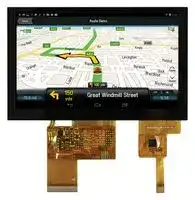
MCT050TC0CW800480LML
TFT LCD, Transmissive, 5
⚠️ Reference pricing provided. In case of supply shortages, we will connect you with our trusted procurement partners to ensure your project's continuity.
- Manufacturer: MIDAS
- Product type: TFT LCD Displays
- Resolution: 800 x 480 Pixels
- Module Size: 120.7mm x 75.8mm
- Touchscreen: Capacitive Touch
- Display Size: 5"
- Logic Voltage: 3.3V
- Display Pinout: 40 Way FPC
- Interface Type: RGB
- Display Appearance: RGB
- Display Brightness: 350cd/m²
- Display Orientation: Landscape
- Operating Temperature Max: 70°C
- Operating Temperature Min: -20°C
| Delivery and price | |
|---|---|
| Units per pack | 50 |
| Price | 45.75 € |
| Current stock | 10+ |
| Lead time | 30 days |
Datasheet

**Midas Components Limited Telephone** +44 (0)1493 602602 Electra House **Fax** +44 (0)1493 665111 32 Southtown Road **Email** sales@midasdisplays.com Great Yarmouth **Website** www.midasdisplays.com Norfolk NR31 0DU England **==> picture [318 x 141] intentionally omitted <==** **----- Start of picture text -----**<br> Specification<br>Part Number:<br>Po MCTOSOTCOCW800480LML<br>Version:<br>ee<br>Date:<br>| 22/06/2016<br>Revision<br>VERSION DATE REVISED PAGE NO. Note<br>0 2016/06/21 First issue<br>**----- End of picture text -----**<br> ## Contents ## 1.Module Classification Information - 2.Summary - 3.General Specification - 4.Interface - 5.Contour Drawing - 6.Absolute Maximum Ratings - 7.Electrical Characteristics 8.Optical Characteristics 9.Reliability 10.Touch Panel Information 11.Other ## **2.Summary** This technical specification applies to 5.0’ color TFT-LCD panel. The 5.0’ color TFT-LCD panel is designed for camcorder, digital camera application and other electronic products which require high quality flat panel displays. This module follows RoHS. # **Midas Active Matrix Display Part Number System** **MC T 057 A 6 * W 320240 L M L * *** 1 2 3 4 5 6 7 8 9 10 11 12 13 - 1 = MC: Midas Components 2 = T: TFT A: Active Matrix OLED M: Monitor - 3 = Size - 4 = Series - 5 = - Viewing Angle: 6: 6 O’clock 12: 12 O’clock O: All Round Viewing Angle - 6 = Blank: No Touch T: Resistive Touchscreen C: Capacitive Touchscreen = Operating Temp Range: S: 0+50Deg C B: -20+60Deg C W: -20+70Deg C E: -30+85Deg C X: -30+80Deg C - 7 - No of Pixels - 8 = No of Pixels 9 = Orientation: P: Portrait L: Landscape - 10 = - Mode: R: Reflective M: Transmissive T: Transflective - S: Sunlight Readable (Transmissive) W: White on Black (Monochrome) - 11 = - Backlight: Blank: None L: LED C: CCFL - 12 = Blank: No Module/board C: Controller board module (E-Tech) 13 = Blank: None OB: Optically Bonded IPS: In‐plane switching ## **3. General Specifications** - Size: 5.0 inch - Dot Matrix: 800× 3(RGB) × 480 dots - Module dimension: 120.7×75.8 ×4.475 mm - Active area: 108.0×64.8 mm - Dot pitch: 0.135 x 0.135 mm - LCD type: TFT, Normally White, Transmissive - View Direction: 12 o’clock - Gray Scale Inversion Direction: 6 o’clock - CTP FW Version: A - Backlight Type: LED ,Normally White - With /Without TP: With CTP - Surface: Glare *Color tone slight changed by temperature and driving voltage. ## **4. Interface** ## **4.1. LCM PIN Definition** FPC Connector is used for the module electronics interface. The recommended model is FH19SC-40S-0.5SH manufactured by HIROSE. |**Pin**|**Symbol**|**Function**|**Remark**| |---|---|---|---| |1|VLED-|Power for LED backlight (Cathode)|| |2|VLED+|Power for LED backlight (Anode)|| |3|GND|Power Ground|| |4|VDD|Power voltage|| |5|R0|Red data (LSB)|| |6|R1|Red data|| |7|R2|Red data|| |8|R3|Red data|| |9|R4|Red data|| |10|R5|Red data|| |11|R6|Red data|| |12|R7|Red data(MSB)|| |13|G0|Green data(LSB)|| |14|G1|Green data|| |15|G2|Green data|| |16|G3|Green data|| |17|G4|Green data|| |18|G5|Green data|| |19|G6|Green data|| |20|G7|Green data(MSB)|| |21|B0|Blue data(LSB)|| |22|B1|Blue data|| |23|B2|Blue data|| |24|B3|Blue data|| |25|B4|Blue data|| |26|B5|Blue data|| |27|B6|Blue data|| |28|B7|Blue data(MSB)|| |29|GND|Power Ground|| |30|CLK|Sample clock|| |31|DISP|Display on/off|| |32|HSYNC Horizontal s|HSYNC Horizontal sync input|| |33|VSYNC Vertical sync input|VSYNC Vertical sync input|| |34|DE|Data input enable|| |35|NC|No connection|| |36|GND|Power Ground|| |37|NC|No connection|| |38|NC|No connection|| |39|NC|No connection|| |40|NC|No connection|| ## **CTP PIN Definition** |**Pin**|**Symbol**|**Function**|**Remark**| |---|---|---|---| |1|**Symbol**<br>VSS|Ground for analog circuit|| |2|VDDT|Power Supply: +3.3V|| |3|SCL|I2C clock input|| |4|NC|No connect|| |5|SDA|I2C datainput and output|| |6|NC|No connect|| |7|/RST|External Reset, Low is active|| |8|/WAKE|External interrupt from the host|| |9|/INT|External interrupt to the host|| |10|VSS|Ground for analogcircuit|| ## **5. Contour Drawing** **==> picture [400 x 337] intentionally omitted <==** **----- Start of picture text -----**<br> PINNO, SYMBOL’ PINNO, SYMBOL PINNO. SYMBOL<br>1 VSS 1 VLED- 21 B0<br>120.7¡ À0.3 2 VDDT 2 VLED+ 22 B1<br>TP_Outline 119.7 0.5¡ À0.5 3 SCL 3 GND 23 B2<br>TP_VA 109.0TP_AA 110.0 6.155.65 45 SDANC 4 VDD 24 B3<br>TFT_AA 108 6.4 4.475¡ À0.5 6 NC 5 R0 25 B4<br>7 /RST 6 R1 26 B5<br>8 /WAKE 7 R2 27 B6<br>9 /INT 8 R3 28 B7<br>10 VSS<br>9 R4 29 GND<br>10 R5 30 CLK<br>11 R6 31 DISP<br>800RGB X 480 12 R7 32 HSync<br>13 G0 33 VSync<br>Display center 14 G1 34 DE<br>15 G2 35 NC<br>16 G3 36 GND<br>Black printing<br>17 G4 37 NC<br>18 G5 38 NC<br>19 G6 39 NC<br>1.65 Max<br>Le t h oy Yj, COMPONENT HEIGHT 20 G7 40 NC<br>26.3¡À0.5 K A<br>0.135<br>0.045<br>13.55 RGBRGB<br>' | , | 4 I , Contact side Al| Stiffener !i t RGBRGB t<br>1 40 10 1<br>P0.5*39=19.5 i 0.35 P0.5*9=4.50.35 0.3¡À0.05 0.3¡ À0.05 SCALE 30/1<br>20.5¡À0.1 5.5 A<br>16.15¡À0.5 The non-specified tolerance of dimension is 0.3mm.<br>A i eile, K<br>CIRCUIT DIAGRAM : 6*3 Dice<br>0.6¡ À0.5 2.8 3.3 3.42<br>AA 66.1 _ VA 65.1 _<br>75.8¡ À0.3 Outline 75.2 _ TP TP TFT_AA 64.8<br>TP<br>5.82<br> À0.5<br>48.6¡ À0.5 9.5¡4 0.135<br>3.5 4<br>5<br>**----- End of picture text -----**<br> ## **6. Absolute Maximum Ratings** |**Item**|**Symbol**|**Min**|**Typ**|**Max**|**Unit**| |---|---|---|---|---|---| |Operating Temperature|TOP|-20|-|+70|| |Storage Temperature|TST|-30|-|+80|| Note: Device is subject to be damaged permanently if stresses beyond those absolute maximum ratings listed above 1. > **==> picture [134 x 108] intentionally omitted <==** **----- Start of picture text -----**<br> Ambient Tem. vs Alloeable Forward Curren<br>40<br>30<br>20<br>10<br>00 20 40 60 80 100<br>Ambient Temperature(oC)<br>Alloeable Forward Current IF(mA)<br>**----- End of picture text -----**<br> ## **7. Electrical Characteristics 7.1. Typical Operation Conditions** |**Item**|**Symbol**|**Values**|**Values**|**Values**|**Unit**|**Remark**| |---|---|---|---|---|---|---| |||**Min.**|**Typ. **|**Max.**||| |Power voltage|VDD|3.1|3.3|3.5|V|| |Current for Driver(Black)|Idd|-|110|170|mA VDD=3.3V|mA VDD=3.3V| |Input logic high voltage|VIH|0.7 VDD|-|VDD|V|Note 1| |Input logic low voltage|VIL|0|-|0.3 VDD||| Note1: CLK,DE,R0~R7, G0~7, B0~7. ## **7.2. Backlight Driving Conditions** |**Item**|**Symbol**|**Values**|**Values**|**Values**|**Unit**|**Remark**| |---|---|---|---|---|---|---| |||**Min.**|**Typ.**|**Max.**||| |Voltage for LED backlight|VL|18|19.2|20|V|Note 1| |Current for LED backlight|IL|--|60|--|mA|| |LED life time|-|--|50,000|-|Hr|Note 2| Note 1: The LED Supply Voltage is defined by the number of LED at Ta=25 ℃ and IL =20ma/pcs. Note 2: The “LED life time” is defined as the module brightness decrease to 50% Original brightness at Ta=25 ℃ and IL =20mA/pcs. The LED lifetime could be decreased if operating IL is lager than 25mA/pcs. ## **7.3. Power Sequence** To prevent a latch-up or DC operation of the LCD module, the power on/off sequence should be as the diagram below. Voo POWER SUPPLY INTERFACE SIGNAL ## **7.4. Timing Characteristics** Timing conditions Parallel DE mode RGB input timing table |**Parameter**|**Symbol**|**Values**|**Values**|**Values**|**Unit**|**Remark**| |---|---|---|---|---|---|---| |||**Min.**|**Typ.**|**Max.**||| |CLK frequency|Fclk|26.4|33.3|46.8|MHz|| |DEV period time|Tv|510|525|650|H|| |DEV display area|Tvd|480|||H|| |DEV blanking|Tvd|30|45|170|H|| |DEH period time|Th|862|1056|1200|CLK|| |DEH display area|Thd|800|||CLK|| |DEH blanking|THb|62|256|400|CLK|| |CLK cycle time|Tclk|21.3|30|37.8|ns|| |Clock width of high level|Tcwh|40|50|60|%|| |Clock width of low level|Tcwl|40|50|60|%|| |Clock rising time|Trck|8|-|-|ns|| |Clock falling time|Tfck|8|-|-|ns|| |Data Setup Time|Tdasu|8|-|-|ns|| |Data Hold Time|Tdahd|8|-|-|ns|| |DE Setup Time|Tdesu|8|-|-|ns|| |DE Hold Time|Tdehd|8|-|-|ns|| ## 7.5. **Timing diagram** **==> picture [122 x 59] intentionally omitted <==** **----- Start of picture text -----**<br> DATA<br>voi} sool VOT<br>**----- End of picture text -----**<br> ## **8. Optical Characteristics** |**Item**|**Item**|**Symbol**|**Condition.**|**Min**|**Typ.**|**Max.**|**Unit**|**Remark**| |---|---|---|---|---|---|---|---|---| |Response time||Tr|θ=0°、Φ=0°|-|10|20|.ms|Note 3,5| |||Tf||-|15|30|.ms|| |Contrast ratio||CR|At optimized<br>viewing angle|400|400<br>500|-|-|Note 4,5| |Color<br>Chromaticity|White|Wx|θ=0°、Φ=0|0.26|0.31|0.36||Note 2,6,7| |||Wy||0.28|0.33|0.38||| |Viewing angle<br>(Gray Scale<br>Inversion<br>Direction)|Hor.|ΘR|CR≧10|-|75|-|Deg.|Note 1| |||ΘL||-|75|-||| ||Ver.|ΦT||-|75|-||| |||ΦB||-|75|-||| |Brightness||-|-|250|250<br>350|-|cd/<br>㎡|Center of<br>display| Note 1: Definition of viewing angle range Fig. 8.1. Definition of viewing angle Note 2: Test equipment setup: After stabilizing and leaving the panel alone at a driven temperature for 10 minutes, the measurement should be executed. Measurement should be executed in a stable, windless, and dark room. Optical specifications are measured by Topcon BM-7or BM-5 luminance meter 1.0° field of view at a distance of 50cm and normal direction. Fig. 8.2. Optical measurement system setup Note 3: Definition of Response time: The response time is defined as the LCD optical switching time interval between “White” state and “Black” state. Rise time, Tr, is the time between photo detector output intensity changed from 90%to 10%. And fall time, Tf, is the time between photo detector output intensity changed from 10%to 90% **==> picture [377 x 81] intentionally omitted <==** **----- Start of picture text -----**<br> D is p la y<br>D a ta W h ite (T F T O F F ) B la c k (T F T O N ) W h ite (T F T O F F )<br>ie |<br>1 0 0 %<br>S 9 0 % C t s ~ a _<br>a<br>2 |<br>Ss<br>a!<br>1 0 %<br>=! 0 % y .<br>**----- End of picture text -----**<br> Note 4: Definition of contrast ratio: The contrast ratio is defined as the following expression. Luminance measured when LCD on the "White" state Contrast ratio (CR) = Luminance measured when LCD on the "Black" state Note 5: White Vi = Vi50 ± 1.5V Black Vi = Vi50 ± 2.0V “±” means that the analog input signal swings in phase with VCOM signal. “±” means that the analog input signal swings out of phase with VCOM signal. The 100% transmission is defined as the transmission of LCD panel when all the input terminals of module are electrically opened. Note 6: Definition of color chromaticity (CIE 1931) Color coordinates measured at the center point of LCD Note 7: Measured at the center area of the panel when all the input terminals of LCD panel are electrically opened. ## **9. Reliability** **Environmental Test** **==> picture [472 x 379] intentionally omitted <==** **----- Start of picture text -----**<br> |||||||| |---|---|---|---|---|---|---| |DG|Test Item|Content|of Test|Test|Condition|Note| |High Temperature|Endurance test applying the high storage temperature|2| |a|storage|ee|for a long time.|200hrs| |Low Temperature|Endurance test applying the low storage temperature|1,2| |a|storage|for a long time.|200hrs| |High Temperature|Endurance test applying the electric stress (Voltage &|——| |Operation|Current) and the thermal stress to the element for a|200hrs| |long time.| |Low Temperature|Endurance test applying the electric stress under low|1| |a|Operation|temperature for a long time.|200hrs| |High Temperature/|The module should be allowed to stand at|1,2| |Humidity|Operation|6001,90%RH|max|96hrs| |Thermal shock|The sample should be allowed stand the following 10|-2011/7001|——| |resistance|cycles of|10 cycles| |operation| |-2000|250|700| |30min 5min 30min| |1 cycle| |Vibration test|Endurance test applying the vibration during|Total fixed amplitude : 3| |transportation and using.|15mm| |Vibration Frequency :| |10~55Hz| |One cycle 60| |seconds to 3| |directions of X,Y,Z for| |Each 15 minutes| |Static electricity test|Endurance test applying the electric stress to the|VS=±600V(contact)|——| |terminal.|,±800v(air),| |RS=330Ω| |CS=150pF| |10 times| **----- End of picture text -----**<br> Note1: No dew condensation to be observed. Note2: The function test shall be conducted after 4 hours storage at the normal Temperature and humidity after remove from the test chamber. Note3: The packing have to including into the vibration testing. ## **10. Touch Panel Information** **==> picture [460 x 260] intentionally omitted <==** **----- Start of picture text -----**<br> 1.675¡ Ó0.15(w ith D ouble side adhesive) 118.90(D ouble side adhesive)<br>TP O utline 119.70TP A A 110.00TP V A 109.00 C over G lass: 0.70¡LO C A:0.175¡ITO G lass: 0.70¡Ó0.05Ó0.05Ó0.05 3.60 111.80(D ouble side adhesive)110.00 AA109.00 VA 3.50<br>ee ]SSaa (0,0) ST1a |<br>Pull tape ‘<br>3M 467 Pull tape<br>Double side adhesive<br>T=0.1mm<br>Black printing.<br>ro r L "vy<br>1<br>|<br>M A X 1.50<br>98.55 0.1¡ Ó0.05 BACK V IEW<br>1 L 10 : | 1 - 1 10 1<br>tr2b 0.500.35P0.5*9=4.50 | | 0.30¡ Ó0.05 — Ea 5.50 | PINNO. SYMBOL<br>FRO N T V IEW<br>1 V SS<br>2 V D D T<br>3 SCL<br>The non-specified tolerance of dim ension is 0.2m m . 4 N C<br>5 SD A<br>6 N C<br>aia 87 /W A KE/RST<br>9 /IN T<br>10 V SS<br>4-R0.50 1.38<br>TP Outline 75.20 TP AA 66.10 TP VA 65.10 65.10 VA 66.10 AA<br>68.12(Double side adhesive) 73.80(Double side adhesive)<br>FRONT VIEW BACK VIEW<br>4.30<br>49.50<br>4.00<br>Contact side Stiffener<br>6.00<br>**----- End of picture text -----**<br> ## **10.1. CTP I2C Timing:** I2C Serial Data Transfer Format I2C master write, slave read I2C master read, slave write |**Mnemonics**|**Description**| |---|---| |S|12C Start or 12C Restart| |A[6:0]|Slave address| |R/W|READ/WRITE bit,‘1' for read,‘0' for write| |A(N)|ACK(NACK)bit| |P|STOP :the indication of the end of a packet(if this bit is missing, S will<br>indicate the end of the current packet and beginningof the next packet)| Lists the meanings of the mnemonics used in the above figures |**Parameter**|**Unit**|**Min**|**Max**| |---|---|---|---| |SCL frequency|KHz|0|400| |Bus free time between a STOP and START condition|us|4.7|\| |Hold time(repeated)ST ART condition|us|4.0|\| |Data setuptime|ns|250|\| |Setuptime for a repeated START condition|us|4.7|\| |Setuptime for STOP condition|us|4.0|\| Interface Timing Characteristics AS FOR STANDARD CTPM, HOST NEED TO USE BOTH INTERRUPT CONTROL SIGNAL AND SERIAL DATA INTERFACE TO GET THE TOUCH DATA. HERE IS THE TIMING TO GET TOUCH DATA. ## **10.2. WRITE BYTES TO I2C SLAVE** AS FOR STANDARD CTPM, HOST NEED TO USE BOTH INTERRUPT CONTROL SIGNAL AND SERIAL DATA INTERFACE TO GET THE TOUCH DATA, HERE IS THE TIMING TO GET TOUCH DATA. Serial ## Address: 0x38 ## TOUCH DATA READ PROTOCOL |NAME|VALUE|DESCRIPTION| |---|---|---| |START CH|0X00|START COMMAND FOR CTPM TOUCH DATA PACKET,HOST<br>MUST SEND CTPM A START CH COMMAND BEFORE READ<br>TOUCH DATA| |lst READ BYTE~<br>LAST READ BYTE||TOUCH DATA PACKET<br>SENT BY CTPM,EACH BYTE HAS 8-BIT DATA ,A TOUCH DATA<br>PACKET CONSISTS OF N BYTE| A DATA PACKET STARTS WITH A HEADER AND ENDS WITH CRC CODE,AS FOR 5 POINTS DATA PACKET,THE LENGTH OF THE PACKET IS ALWAYS 26 BYTES IN SPITE OF ACTUAL TOUCH POINTS. |**Address**|**Name**|**Bit7 Bit6**|**Bit7 Bit6**|**Bit5**|**Bit4**|**Bit3**|**Bit2**|**Bit1 Bit0**|**Bit1 Bit0**|**Bit1 Bit0**|**Host**<br>**Access**| |---|---|---|---|---|---|---|---|---|---|---|---| |00h|Devide_Mode||Device Model[2:0]|||||||RW|| |01h|Gest_ID|Gesture ID[7:0]||||||||R|| |02h|TD_Status|||||Number of<br>touchpoints[3:0]||||R|| |03h|Touch1_XH|1st Event<br>Flag||||1stTouch<br>X Position[11:8]||||R|| |04h|Touch1_XL|1stTouch X Position[7:0]||||||||R|| |05h|Touch1_YH|1st Touch ID[3:0]||||1st Touch<br>Y Position[11:8]||||R|| |06h|Touch1_YL|1st Touch Y Position[7:0]||||||||R|| |09h|Touch2_XH|2ndEvent<br>Flag||||2ndTouch<br>X Position[11:8]||||R|| |0Ah|Touch2_XL|2nd Touch X Position[7:0]||||||||R|| |0Fh<br>~~pt~~<br>|Touch3_XH<br>~~ptef~~<br>|3rdEvent<br>Flag<br>~~ef~~<br>|<br>~~ef~~<br>|3rdTouch<br>X Position[11:8]<br>~~ef~~<br>~~=~~|R<br>~~ef~~<br>~~=~~| |---|---|---|---|---|---| |10h<br>~~pt~~<br>~~SSS~~|Touch3_XL<br>~~pt~~<br>~~SSS~~|3rd Touch X Position[7:0]<br><br>~~SSS=~~|||R<br><br>~~SSS=~~| |11h<br>~~SSS~~|Touch3_YH<br>~~SSS~~|3rdTouch ID[3:0]<br>~~SSS~~||3rdTouch<br>Y Position[11:8]<br>~~SSS=~~|R<br>~~SSS=~~| |12h<br>~~SSS~~|Touch3_YL<br>~~SSS~~|3rd Touch Y Position[7:0]<br>~~SSS=~~|||R<br>~~SSS=~~| |15h<br>~~SSS~~|Touch4_XH<br>~~SSS~~|4thEvent<br>Flag<br>~~SSS~~|<br>~~SSS~~|4thTouch<br>X Position[11:8]<br>~~SSS=~~|R<br>~~SSS=~~| |16h|Touch4_XL|4th Touch X Position[7:0]|||R| |17h|Touch4_YH|4thTouch ID[3:0]||4thTouch<br>Y Position[11:8]|R| |18h|Touch4_YL|4th Touch Y Position[7:0]|||R| |1Bh|Touch5_XH|5thEvent<br>Flag||5thTouch<br>X Position[11:8]|R| |1Ch|Touch5_XL|5th Touch X Position[7:0]|||R| |1Dh|Touch5_YH|5thTouch ID[3:0]||5thTouch<br>Y Position[11:8]|R| |1Eh|Touch5_YL|5th Touch Y Position[7:0]|||R|
Updated at February 9, 2023
About Novapart
Novapart is a B2B electronic component broker specialising in stock shortages and cost reduction. We source hard-to-find parts and identify compliant alternatives across a catalogue of 410,000+ components from 500+ manufacturers.
Learn more →Stock Shortage Specialist
When a component is unavailable, discontinued or has an unacceptable lead time, we tap into our network of vetted European and Asian distributors to source what you need — without compromising on quality or traceability.
Request a quote →Compliant Alternatives
We identify pin-to-pin, electrically equivalent substitutes that meet the same certifications (RoHS, AEC-Q100, REACH) as your original specification — validated against datasheets, not just part numbers. Often at a lower cost.
BOM Analysis service →