
Image not available
Illustrative purposes only

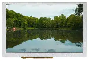
MCT050ACA0W800480LML
TFT LCD, 5
⚠️ Reference pricing provided. In case of supply shortages, we will connect you with our trusted procurement partners to ensure your project's continuity.
- Manufacturer: MIDAS
- Product type: TFT LCD Displays
- VGA Size: WVGA
- Resolution: 800 x 480 Pixels
- Module Size: 120.7mm x 75.8mm
- Touchscreen: No Touchscreen
- Display Size: 5"
- Logic Voltage: 3.3V
- Display Pinout: 36 Way FPC
- Interface Type: Parallel
- Display Appearance: RGB
- Display Brightness: 400cd/m²
- Display Orientation: Landscape
- Operating Temperature Max: 70°C
- Operating Temperature Min: -20°C
| Delivery and price | |
|---|---|
| Units per pack | 50 |
| Price | 44.67 € |
| Current stock | 10+ |
| Lead time | 30 days |
Datasheet

**Midas Components Limited Telephone** +44 (0)1493 602602 Electra House **Fax** +44 (0)1493 665111 32 Southtown Road **Email** sales@midasdisplays.com Great Yarmouth **Website** www.midasdisplays.com Norfolk NR31 0DU England **Specification** Part Number: ~~Po MCTO50ACAOW800480LML~~ Version: ~~ee~~ Date: ~~| 27/07/2016~~ **Revision VERSION DATE REVISED PAGE NO. Note** 0 2016/07/26 First issue ## Contents ## 1.Module Classification Information 2.Summary - 3.General Specification 4.Interface - 5.Contour Drawing - 6.Block Diagram 7.Absolute Maximum Ratings 8.Electrical Characteristics 9.DC Characteristics 10.Interface Timing Characteristics 11.Optical Characteristics 12.Reliability 13.Other ## **2.Summary** This technical specification applies to 5.0’ color TFT-LCD panel. The 5.0’ color TFT-LCD panel is designed for camcorder, digital camera application and other electronic products which require high quality flat panel displays. This module follows RoHS. ## **3.General Specifications** - Size: 5.0 inch - Dot Matrix: 800 × 3(RGB) × 480 dots - Module dimension: 120.7 x 75.8 x 8.0 mm - Active area: 108.0 x 64.8 mm - Dot pitch: 0.045 x 0.135 mm - LCD type: TFT, Normally White, Transmissive - View Direction: 12 o’clock - Gray Scale Inversion Direction: 6 o’clock - Backlight Type: LED, Normally White - Controller IC: SSD1963 - Interface: Digital 8080 family MPU 8bit/16bit - With /Without TP: Without TP Surface: Anti-Glare *Color tone slight changed by temperature and driving voltage. # **Midas Active Matrix Display Part Number System** **MC T 057 A 6 * W 320240 L M L * *** 1 2 3 4 5 6 7 8 9 10 11 12 13 - 1 = MC: Midas Components 2 = T: TFT A: Active Matrix OLED M: Monitor - 3 = Size - 4 = Series - 5 = - Viewing Angle: 6: 6 O’clock 12: 12 O’clock O: All Round Viewing Angle - 6 = Blank: No Touch T: Resistive Touchscreen C: Capacitive Touchscreen = Operating Temp Range: S: 0+50Deg C B: -20+60Deg C W: -20+70Deg C E: -30+85Deg C X: -30+80Deg C - 7 - No of Pixels - 8 = No of Pixels 9 = Orientation: P: Portrait L: Landscape - 10 = - Mode: R: Reflective M: Transmissive T: Transflective - S: Sunlight Readable (Transmissive) W: White on Black (Monochrome) - 11 = - Backlight: Blank: None L: LED C: CCFL - 12 = Blank: No Module/board C: Controller board module (E-Tech) 13 = Blank: None OB: Optically Bonded IPS: In‐plane switching ## **4.Interface** ## **4.1. LCM PIN Definition (CON3)** |**Pin**|**Symbol Function**|**Symbol Function**|**Remark**| |---|---|---|---| |1|GND|System round pin of the IC.<br>Connect to system ground.|| |2|VDD|Power Supply :+3.3V|| |3|BL_E|Backlight control signal , H: On \ L: Off|| |4|D/C|Data/Command select|| |5|WR|Write strobe signal|| |6|RD|Read strobe signal|| |7|DB0|Data bus|| |8|DB1|Data bus|| |9|DB2|Data bus|| |10|DB3|Data bus|| |11|DB4|Data bus|| |12|DB5|Data bus|| |13|DB6|Data bus|| |14|DB7|Data bus|| |15|DB8|Data bus (When select 8bits mode, this pin is NC)|Note1| |16|DB9|Data bus (When select 8bits mode, this pin is NC)|Note1| |17|DB10|Data bus (When select 8bits mode, this pin is NC)|Note1| |18|DB11|Data bus (When select 8bits mode, this pin is NC)|Note1| |19|DB12|Data bus (When select 8bits mode, this pin is NC)|Note1| |20|DB13|Data bus (When select 8bits mode, this pin is NC)|Note1| |21|DB14|Data bus (When select 8bits mode, this pin is NC)|Note1| |22|DB15|Data bus (When select 8bits mode, this pin is NC)|Note1| |23|NC|No connection|| |24|NC|No connection|| |25|CS|Chip select|| |26|RST|Hardware reset|| |27|NC|No connection|| |28|NC|No connection|| |29|NC|No connection|| |30|NC|No connection|| |31|NC|No connection|| |32|NC|No connection|| |33|VLED-|VLED-for B/L LED inverter (GND)|| |34|VLED-|VLED-for B/L LED inverter (GND)|| |35|VLED+|VLED+for B/L LED inverter (+5V)|| |36|VLED+|VLED+ for B/L LED inverter(+5V)|| ## **5.Contour Drawing** **==> picture [399 x 342] intentionally omitted <==** **----- Start of picture text -----**<br> 120.7¡ À0.3<br>110.7(Bezel open)¡À0.3 5.00<br>110.0¡À0.3(Top pol) 5.45 8.00 Max<br>108.0(AA) 6.40 6.3¡ À0.5<br>2.8¡ À0.2<br>1.00<br>Display center _<br>|<br>rot<br>; y a, i!<br>0.135<br>0.045<br>ie<br>RGBRGB<br>RGBRGB<br>di t t:<br>SCALE 30/1 The non-specified tolerance of dimension is 0.3mm.<br>CIRCUIT DIAGRAM : 6*3 Dice<br>2.01 2.31 3.42<br>75.8¡ À0.3 64.8(AA)<br>67.0¡ À0.3(Top pol)<br>67.4(Bezel open)¡ À0.3<br>0.135<br>**----- End of picture text -----**<br> |Pin|Symbol||||||||||||||||||||||||||||||||||||||||||||||||||||||||||||||| |---|---|---|---|---|---|---|---|---|---|---|---|---|---|---|---|---|---|---|---|---|---|---|---|---|---|---|---|---|---|---|---|---|---|---|---|---|---|---|---|---|---|---|---|---|---|---|---|---|---|---|---|---|---|---|---|---|---|---|---|---|---|---|---| |1<br>2|GND<br>VDD|||1.0|||||||||||||||||||118.70¡À0.5PCB||||||||||||||||||||||||||||||||||||||||| |3|BLE|0.2|||||12.39||||||||||||||||||||||||||||||||||||||||||||||||||||||||| |4|D/C||||||||||||||||||||||||||||||||||||||||||||||||||||||||||||||| |5<br>6<br>7<br>8<br>9<br>10<br>11<br>12|WR<br>RD<br>DB0<br>DB1<br>DB2<br>DB3<br>DB4<br>DB5|45.00¡ À0.5PCB|11.9|~~!~~||||1<br>36<br>1<br>He~~re~~<br>~~,~~<br>~~ar~~||||||||CON3<br>10<br>CON2<br>(Down-Side)<br>CN-FPC-36P/P0.5|||||||||||||||||||||||CON1<br>1<br>40<br>~~=~~|||||||||||||||||||25.60|Y|i|||| |13|DB6||||||||||||||||||||||||||||||||||||||||||||||||||||||||||||||| |14<br>15<br>16<br>17|DB7<br>DB8<br>DB9<br>DB10|||||||||||||||||||||||||||||||||||||||||||||||||||||||||||45.00¡ À1.0||3-? 1.6NPTH|| |18|DB11||||||||||||||||||||||||||||||||||||||||||||||||||||||||||||||| |19<br>20<br>21|DB12<br>DB13<br>DB14||||||||||||||||||||||~~_PE~~||||||||||||||||||||||||||||||||||||||||| |22|DB15||||||||||||||||||||||||||||||||||||||||||||||||||||||||||||||| |23|NC||||||||||||||||||||||||||||||||||||||||||||||||||||||||||||||| |24|NC||||||||||||||||||||||||||||||||||||||||||||||||||||||||||||||| |25|CS||||||||||||||||||||||||||||||||||||||||||||||||||||||||||||||| |26|RST||||||||||||||||||||||||||||||||||||||||||||||||||||||||||||||| |27|NC||||||||||||||||||||||||||||||||||||||||||||||||||||||||||||||| |28|NC||||||||||||||||||||||||||||||||||||||||||||||||||||||||||||||| |29|NC||||||||||||||||||||||||||||||||||||||||||||||||||||||||||||||| |30|NC||||||||||||||||||||||||||||||||||||||||||||||||||||||||||||||| |31|NC||||||||||||||||||||||||||||||||||||||||||||||||||||||||||||||| |32|NC||||||||||||||||||||||||||||||||||||||||||||||||||||||||||||||| |33<br>34|VLED-<br>VLED-|||||||||||||||||||||||||||||||||||||||||||||||||||||||||||The non-specified tolerance of dimension is||The non-specified tolerance of dimension is|0.3mm.| |35|VLED+||||||||||||||||||||||||||||||||||||||||||||||||||||||||||||||| |36|VLED+||||||||||||||||||||||||||||||||||||||||||||||||||||||||||||||| ## **6.Block Diagram** **==> picture [477 x 282] intentionally omitted <==** **----- Start of picture text -----**<br> User<br>Control board LCD Panel<br>Connector<br>Power supply VDD,GND a SSD1963 VDD L a VCC<br>ControlSignal D/C#RD#(E)C/S# === MCU emg Registers<br>If 16 bit [15:0]If 8 bit [7:0] Data BusWR#(R/W) == Interface — = LSHIFTLDATA 〔 23 == : 0 > 〕 PLCKRGB 24 Bit<br>LCD<br>LDEN = DE<br>Controller =<br>Frame Buffer e el RST = RESET<br>Reset RST# = System Clock — 5.0"<br>and Reset Mgr<br>800(RGB)x480<br>Rotation/<br>Mirror<br>Clock<br>Generator DBC<br>Backlight Enable BLE <9 S e l H:ON Backlight ON/OFF<br>L:OFF<br>Backlight LED VLED+,VLED- ~ Backlight Backlight LED Output | LED +/- Backlight<br>—— — i > - i<br>IC Voltage IC Controller LED<br>LCD Interface<br>**----- End of picture text -----**<br> ## **7.Absolute Maximum Ratings** |**Item**|**Symbol**|**Min**|**Typ**|**Max**|**Unit**| |---|---|---|---|---|---| |Operating Temperature|TOP|-20|-|+70|| |Storage Temperature|TST|-30|-|+80|| Note: Device is subject to be damaged permanently if stresses beyond those absolute maximum ratings listed above 1. > **==> picture [134 x 108] intentionally omitted <==** **----- Start of picture text -----**<br> Ambient Tem. vs Alloeable Forward Curren<br>40<br>30<br>20<br>10<br>00 20 40 60 80 100<br>Ambient Temperature(oC)<br>Alloeable Forward Current IF(mA)<br>**----- End of picture text -----**<br> ## **8.Electrical Characteristics** **8.1. Operating conditions: (CON3.Pin1=GND, Pin2=VDD) Item Symbol Condition Min Typ Max Unit Remark** - - Supply Voltage For LCM VDD 3.0 3.1 3.3 V Supply Current For LCM IDD — — 150 230 mA Note1 ~~FEE~~ Note 1 : This value is test for VDD =3.3V , Ta=25 ℃ only **8.2. Backlight driving conditions (CON3.Pin33,34=VLED-, Pin35,36=VLED+) Parameter Symbol Min. Typ. Max. Unit Remark** Operation Current For LED VLED=5V 200 - 300 mA Note 1,2 Driver Supply Voltage For LED Driver VLED+ - 5 - V - Note LED Life Time 50,000 - Hr 2,3,4 ~~Sata~~ Note 1 : Base on VLED=5.0V for the back light driver IC specification Note 2 : Ta = 25 ℃ Note 3 : Brightness to be decreased to 50% of the initial value Note 4 : The single LED lamp case ## **9.DC CHARATERISTICS** |**Parameter**|**Symbol**|**Rating**|**Rating**|**Rating**|**Unit**|**Condition**| |---|---|---|---|---|---|---| |||**Min**|**Typ**|**Max**||| |Low level input voltage|VIL|0|-|0.3VDD|V|| |High level input voltage|High level input voltage<br>VIH|0.7VDD|-|VDD|V|| ## **10.Interface timing** ## **10.1. 8080 Mode 8bit/16bit** The 8080 mode MCU interface consist of CS#, D/C#, RD#, WR#, Data Bus signals. This interface use WR# to define a write cycle and RD# for read cycle. If the WR# goes low when the CS# signal is low, the data or command will be latched into the system at the rising edge of WR#. Similarly, the read cycle will start when RD# goes low and end at the rising edge of RD#. ## **10.2. 8080 Mode Write Cycle** |**Symbol**<br>~~a~~|**Parameter**<br>~~a~~|**Min**<br>~~a~~|**Typ**<br>~~a~~|**Max**<br>~~a~~|**Unit**<br>~~a~~| |---|---|---|---|---|---| |fMCLK<br>~~a~~<br>~~es~~|System Clock Frequency<br>~~a~~|1<br>~~a~~|-<br>~~a~~|110<br>~~a~~|MHz<br>~~a~~| |tMCLK<br>~~a~~<br>~~es~~|System Clock Period<br>~~a~~|1/ fMCLK<br>~~a~~|-<br>~~a~~|-<br>~~a~~|ns<br>~~a~~| |tPWCSH<br>~~es~~|Control Pulse High Width Write<br>Read|13<br>30|1.5***t**MCLK<br>3.5***t**MCLK|-|ns| |tPWCSL<br>~~RR~~|tPWCSL<br>Control Pulse Low Width Write (next write<br>cycle)<br>Write (next read<br>cycle)<br>Read<br>|13<br>80<br>80<br>|1.5***t**MCLK<br>9***t**MCLK<br>9***t**MCLK<br>|-<br>|ns<br>| |tAS<br>~~RR~~<br>~~A~~|Address SetupTime<br><br>~~2~~|1<br>|-<br>|-<br>|ns<br>| |tAH<br>~~RRre~~<br>~~A~~<br>~~ee~~|Address Hold Time<br>~~re~~<br>~~2~~<br>~~ee,Ve~~|2<br>~~re~~<br>~~Veee~~|-<br>~~re~~<br>~~eeae~~|-<br>~~re~~<br>~~ae~~|ns<br>~~re~~<br>~~eee~~| |tDSW<br>~~re~~<br>~~A~~<br>~~ee~~<br>~~7~~|Write Data SetupTime<br>~~re~~<br>~~2~~<br>~~ee,Ve~~<br>~~ee4~~<br>~~eee~~<br>|4<br>~~re~~<br>~~Veee~~<br>~~a~~<br>~~ee~~|~~re~~<br>~~eeae~~<br>~~ee~~|~~re~~<br>~~ae~~<br>~~eee~~|ns<br>~~re~~<br>~~eee~~<br>~~eee~~| |tDHW<br>~~A~~<br>~~ee~~<br>~~7~~<br>~~7~~|Write Data Hold Time<br>~~2~~<br>~~ee,Ve~~<br>~~ee4~~<br>~~eee~~<br>~~Bh4~~|1<br>~~Veee~~<br>~~a~~<br>~~ee~~<br>~~2eee...~~|-<br>~~eeae~~<br>~~ee~~<br>~~eee...~~|-<br>~~ae~~<br>~~eee~~<br>~~eee...“Se~~|ns<br>~~eee~~<br>~~eee~~<br>~~“Se~~| |tPWLW Write Low Time<br>~~ee~~<br>~~7 ~~<br>~~7~~|tPWLW Write Low Time<br>~~ee, Ve~~<br>~~ee 4~~<br>~~eee ~~<br> ~~Bh4~~<br>~~mY4ee~~|12<br>~~Ve ee~~<br> ~~a~~<br>~~ee~~<br>~~2eee...~~<br>~~Plee~~|~~ee ae~~<br>~~ee~~<br>~~eee...~~<br>~~ee~~<br>~~ee,~~|~~ae ~~<br>~~eee~~<br>~~eee...“Se~~<br>~~ee,~~|ns<br> ~~eee~~<br>~~eee~~<br>~~“Se~~<br>~~ee,ee~~| |tDHR R<br> <br>~~7~~<br>~~rd~~|tDHR ReadDataHoldTime<br> ~~Bh 4~~<br>~~mY4ee~~<br>~~rd 4~~<br>~~eee~~<br>~~A~~|1<br>~~2 eee...~~<br>~~Plee~~<br>~~Aeee~~|-<br>~~eee...~~<br>~~ee~~<br>~~ee,~~<br>~~eeeeee~~|-<br>~~eee... “Se~~<br>~~ee,~~<br>~~eee~~|ns<br>~~“Se~~<br>~~ee,ee~~<br>~~eee~~| |tACC<br>~~rd~~|Access Time<br>~~mY 4 ee~~<br>~~rd 4~~<br>~~eee~~<br>~~A~~|32<br>~~Plee~~<br>~~Aeee~~|~~ee~~<br>~~ee,~~<br>~~eeeeee~~|~~ee,~~<br>~~eee~~|ns<br>~~ee, ee~~<br>~~eee~~| |tPWLR Read Low Time<br>~~rd~~<br>~~a ~~|tPWLR Read Low Time<br>~~rd 4~~<br>~~eee~~<br>~~A~~<br> ~~a~~|36<br>~~A eee~~<br>~~GG~~|-<br>~~eee eee~~<br>~~GG~~|-<br>~~eee~~<br>~~GG~~|ns<br>~~eee~~<br>~~GG~~| |tR<br>~~a~~<br>~~DR~~|Rise Time|-||0.5|ns| |tF<br>~~DR~~<br>~~Po~~<br>~~CO~~|Fall Time<br>~~COESION)@~~|-|-<br>~~SUDDIWV~~|0.5<br>~~SUDDIWV~~|ns<br>~~SUDDIWV|~~| |tCS<br>~~DR~~<br>~~Po~~<br>~~CO~~|Chipselect setuptime<br>~~COESION)@~~<br>~~MMaNUIACTUrFeE/@®~~|2<br>~~MMaNUIACTUrFeE/@®~~|~~MMaNUIACTUrFeE/@®~~<br>~~SUDDIWV~~|-<br>~~MMaNUIACTUrFeE/@®~~<br>~~SUDDIWV~~|ns<br>~~MMaNUIACTUrFeE/@®~~<br>~~SUDDIWV|~~| |tCSH<br>~~Po~~<br>~~CO~~<br>~~Qs~~|Chipselect hold time to read signal<br>~~CO ESION) @~~<br>~~Qs~~|3<br>~~Qs~~|-<br>~~SUDDIWV~~<br>~~Qs~~|-<br>~~SUDDIWV~~<br>~~Qs~~|ns<br>~~SUDDIWV |~~<br>~~Qs~~| ## **10.4. Parallel 8080-series Interface Timing Diagram(Read Cycle)** **10.5. Pixel Data Format** ## **11.Optical Characteristics** |**Item**|**Item**|**Symbol**|**Condition.**|**Min**|**Typ.**|**Max.**|**Unit**|**Remark**| |---|---|---|---|---|---|---|---|---| |Response time||Tr|θ=0°、Φ=0°|-|10|20|.ms|Note 3,5| |||Tf||-|15|30|.ms|| |Contrast ratio||CR|At optimized<br>viewing angle|400|400<br>500|-|-|Note 4,5| |Color<br>Chromaticity|White|Wx|θ=0°、Φ=0|0.26|0.31|0.36||Note 2,6,7| |||Wy||0.28|0.33|0.38||| |Viewing angle|Hor.|ΘR|CR≧10|-|75|-|Deg.|Note 1| |||ΘL||-|75|-||| ||Ver.|ΦT||-|75|-||| |||ΦB||-|75|-||| |Brightness||-|-|300|300<br>400|-|cd/<br>㎡|Center of<br>display| Ta=25±2 ℃, Note 1: Definition of viewing angle range Fig. 11.1. Definition of viewing angle ## Note 2: Test equipment setup: After stabilizing and leaving the panel alone at a driven temperature for 10 minutes, the measurement should be executed. Measurement should be executed in a stable, windless, and dark room. Optical specifications are measured by Topcon BM-7or BM-5 luminance meter 1.0° field of view at a distance of 50cm and normal direction. Fig. 11.2. Optical measurement system setup Note 3: Definition of Response time: The response time is defined as the LCD optical switching time interval between “White” state and “Black” state. Rise time, Tr, is the time between photo detector output intensity changed from 90%to 10%. And fall time, Tf, is the time between photo detector output intensity changed from 10%to 90% **==> picture [382 x 81] intentionally omitted <==** **----- Start of picture text -----**<br> D is p la y<br>D a ta W h ite (T F T O F F ) B la c k (T F T O N ) W h ite (T F T O F F )<br>= 1 0 0 %<br>SsS 9 0 % oF = pai - a o N = = 4<br>8<br>3<br>(=)<br>= 1 0 %<br>a 0 % ==<br>**----- End of picture text -----**<br> Note 4: Definition of contrast ratio: The contrast ratio is defined as the following expression. Luminance measured when LCD on the "White" state Contrast ratio (CR) = Luminance measured when LCD on the "Black" state Note 5: White Vi = Vi50 ± 1.5V Black Vi = Vi50 ± 2.0V “±” means that the analog input signal swings in phase with VCOM signal. “±” means that the analog input signal swings out of phase with VCOM signal. The 100% transmission is defined as the transmission of LCD panel when all the input terminals of module are electrically opened. Note 6: Definition of color chromaticity (CIE 1931) Color coordinates measured at the center point of LCD Note 7: Measured at the center area of the panel when all the input terminals of LCD panel are electrically opened. ## **12.Reliability** |**12.Reliability**<br>Content of Reliability Test (Wide temperature, -20'/~70(1)|**12.Reliability**<br>Content of Reliability Test (Wide temperature, -20'/~70(1)|**12.Reliability**<br>Content of Reliability Test (Wide temperature, -20'/~70(1)|**12.Reliability**<br>Content of Reliability Test (Wide temperature, -20'/~70(1)| |---|---|---|---| |**Environmental Test**<br>~~Ds~~|||| |**Test Item **<br>~~Ds~~|**Content of Test**|**Test Condition **|**Note**| |High Temperature<br>storage<br>~~Ds~~<br>~~a ~~|Endurance test applying the high storage temperature<br>foralongtime.<br> ~~ee~~|200hrs<br>~~ee~~|2<br>~~ee~~| |Low Temperature<br>storage<br>~~a~~|Endurance test applying the low storage temperature<br>foralongtime.<br>~~a~~<br>~~a~~|200hrs<br>~~a~~|1,2| |High Temperature<br>Operation|Endurance test applying the electric stress (Voltage &<br>Current) and the thermal stress to the element for a<br>longtime.|200hrs|——| |Low Temperature<br>Operation<br>~~a~~|Endurance test applying the electric stress under low<br>temperatureforalongtime.<br>~~a~~<br>~~ee~~|200hrs<br>~~ee~~|1<br>~~ee~~| |High Temperature/<br>Humidity Operation|The module should be allowed to stand at<br>6001,90%RH max|96hrs|1,2| |Thermal shock<br>resistance|The sample should be allowed stand the following 10<br>cycles of<br>operation<br>30min 5min 30min<br>1 cycle<br>-2000<br>250<br>700|10 cycles<br>-2011/7001|——| |Vibration test|Endurance test applying the vibration during<br>transportation and using.|Total fixed amplitude :<br>15mm<br>Vibration Frequency :<br>10~55Hz<br>One cycle 60<br>seconds to 3<br>directions of X,Y,Z for<br>Each 15 minutes|Total fixed amplitude :<br>Vibration Frequency :<br>directions of X,Y,Z for<br>3| |Static electricity test|Endurance test applying the electric stress to the<br>terminal.|VS=±600V(contact)<br>,±800v(air),<br>RS=330Ω<br>CS=150pF<br>10 times|——| Note1: No dew condensation to be observed. Note2: The function test shall be conducted after 4 hours storage at the normal Temperature and humidity after remove from the test chamber. Note3: The packing have to including into the vibration testing.
Updated at February 9, 2023
About Novapart
Novapart is a B2B electronic component broker specialising in stock shortages and cost reduction. We source hard-to-find parts and identify compliant alternatives across a catalogue of 410,000+ components from 500+ manufacturers.
Learn more →Stock Shortage Specialist
When a component is unavailable, discontinued or has an unacceptable lead time, we tap into our network of vetted European and Asian distributors to source what you need — without compromising on quality or traceability.
Request a quote →Compliant Alternatives
We identify pin-to-pin, electrically equivalent substitutes that meet the same certifications (RoHS, AEC-Q100, REACH) as your original specification — validated against datasheets, not just part numbers. Often at a lower cost.
BOM Analysis service →