
Image not available
Illustrative purposes only

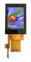
MCT024N0CW240320PMLIPS
TFT LCD, 2.4
⚠️ Reference pricing provided. In case of supply shortages, we will connect you with our trusted procurement partners to ensure your project's continuity.
- Manufacturer: MIDAS
- Product type: TFT LCD Displays
- VGA Size: QVGA
- Resolution: 240 x 320 Pixels
- Module Size: 48.72mm x 70.26mm
- Touchscreen: Capacitive Touch
- Display Size: 2.4"
- Logic Voltage: 3.3V
- Display Pinout: 45 Way FFC
- Interface Type: Parallel
- Display Appearance: RGB
- Display Brightness: 450cd/m²
- Display Orientation: Portrait
- Operating Temperature Max: 70°C
- Operating Temperature Min: -20°C
| Delivery and price | |
|---|---|
| Units per pack | 50 |
| Price | 44.03 € |
| Current stock | 10+ |
| Lead time | 30 days |
Datasheet

**Midas Components Limited Telephone** +44 (0)1493 602602 Electra House **Fax** +44 (0)1493 665111 32 Southtown Road **Email** sales@midasdisplays.com Great Yarmouth **Website** www.midasdisplays.com Norfolk NR31 0DU England

## **Specification**

Part Number: ~~=~~ Version: Date: ~~____foio7/2018~~

## **Revision**

**1.0 2015.07.08 FIRST ISSUE**

## **Contents**

**General Description ------------------------------------------------------------------------------------------------------4 1. Block Diagram -----------------------------------------------------------------------------------------------------------5 2. Outline dimension -----------------------------------------------------------------------------------------------------6 3. Input Terminal Pin Assignment -----------------------------------------------------------------------------------9 4. LCD Optical Characteristics --------------------------------------------------------------------------------------11 5. TFT Electrical Characteristics -----------------------------------------------------------------------------------15 6. TFT AC Characteristic ----------------------------------------------------------------------------------------------17 7. CTP Specification ----------------------------------------------------------------------------------------------------21 8. LCD Module Out-Going Quality Level--------------------------------------------------------------------------27 9. Reliability Test Result -----------------------------------------------------------------------------------------------33 10. Cautions and Handling Precautions -------------------------------------------------------------------------34 11. Packing------------------------------------------------------------------------------------------------------------------35**

## **General Description**

## *** Description**

This is a color active matrix TFT (Thin Film Transistor) LCD (liquid crystal display) that uses amorpho us silicon TFT as a switching device. This model is composed of a Transmissive type TFT-LCD Panel, driver circuit, back-light unit. The resolution of a 2.4’TFT-LCD contains 240*320 pixels, and can displ ay up to 65K/262K colors.

## *** Features**

-Low Input Voltage: 3.3V (TYP)

- -Display Colors of TFT LCD: 65K/262K colors

- TFT Interface: 8/9/16/18BIT 8080 MCU interface

   - 3/4-wire serial interface;

16/18BIT RGB.

- -CTP Interface: I2C

|16/18BIT RGB.<br>Interface: I2C||||
|---|---|---|---|
|**eral Information**<br>**Items**|**Specification**|**Unit**|**Note**|
||**Main Panel**|||
|TFT Display area(AA)|36.72(H)* 48.96(V)<br>(2.4inch)|mm|-|
|CTP View area|37.72(H)* 49.96(V)|mm||
|Driver element|TFT active matrix|-|-|
|Display colors|65K/262K|colors|-|
|Number of pixels|240(RGB)*320|dots|-|
|TFT Pixel arrangement|RGB vertical stripe|-|-|
|Pixel pitch|0.153(H)*0.153(V)|mm|-|
|Viewing angle|ALL|o'clock|-|
|TFT Controller<br>IC|ST7789V|-|-|
|CTP Driver IC|FT6236|||
|Touch mode|Single point and Gestures|||
|Display mode|Transmissive/Normally Black|-|-|
|Operating temperature|-20~+70|℃|-|
|Storage temperature<br>~~===~~|-30~+80<br>~~===~~|℃<br>~~===~~|-<br>~~===~~|


## *** Mechanical Information**

|*** Mechanical Information**|*** Mechanical Information**||||||
|---|---|---|---|---|---|---|
|**Item**||**Min.**|**Typ.**|**Max.**|**Unit**|**Note**|
|Module<br>size|Horizontal(H)||48.72||mm|-|
||Vertical(V)||70.26||mm|-|
||Depth(D)||3.88||mm|-|


Weight TBD g - ~~ee~~ **1. Block Diagram**

## **2. Outline dimension**

## **2.1 LCM**

**==> picture [195 x 55] intentionally omitted <==**

**----- Start of picture text -----**<br>
YeS # SB= #2& BB2 sg 8gs 238 N -<br>2 £ ££ F Sg = sg (eo)<br>S77 2 1 Bee °<br>2s =><br>公差<br>FPC弯折参考图 FPC展开出货<br>**----- End of picture text -----**<br>


## **2.2 CTP**

**==> picture [434 x 598] intentionally omitted <==**

**----- Start of picture text -----**<br>
=a eaada fal<br>Zz AA —<br>“4a—o —=<br>SHAHN MOT TD CO Ww CO oO<br>a oO<br>N<br>oO<br>oO<br>T e r | YT<br>at - - x =<<br>EE oO<br>My i ae O<br>| - Zz<br>' a+ N<br>Lt =aI O(o)a<br>=<br>SS =<br>~<br>' £ &<br>ww !<br>t gat} fo ! ! 3 5<br>(Re = es ee A ;<br>=fad wy &<br>p t 4<br>ry<br>ce<br>Zz<br>—)<br>[ama<br>- - om<br>' iat<br>1 ty<br>1 | ! t ee l<br>SCL SDA INT RST GND<br>公差<br>保护膜手撕位(保证 5mm以上)<br>双面带胶泡棉<br>,<br>℃,<br>℃,<br>    元件面 Component area %<br>℃<br>:≥ : ℃<br>:<br>:<br>:<br>:<br>**----- End of picture text -----**<br>


## **2.3 LCM+CTP**

**==> picture [12 x 489] intentionally omitted <==**

**----- Start of picture text -----**<br>
i<br>1<br>1<br>钢片补强接地 Grounded<br>元件面 Component area<br>**----- End of picture text -----**<br>


**==> picture [5 x 11] intentionally omitted <==**

**----- Start of picture text -----**<br>
公差<br>**----- End of picture text -----**<br>


## **3. Input terminal Pin Assignment**

## **3.1 TFT**

|**3.1 TFT**||||
|---|---|---|---|
|NO.|SYMBOL|DISCRIPTION|I/O|
|1|GND|Ground.|P|
|2|VCI|Supply voltage(3.3V).|P|
|3|VCI|Supply voltage(3.3V).|P|
|4|IM2|MPU Parallel interface bus and serial interface<br>select If use RGB Interface must select serial<br>interface.<br>Fix this pin at VCI and GND.|I|
|5|IM1||I|
|6|IM0||I|
|7|RESET|This signal will reset the device and must be<br>applied to properly initialize the chip.|I|
|8|CS|Chip select input pin (“Low” enable).<br>fix this pin at VCI or GND when not in use.|I|
|9|DC(SCL)|This pin is used to select “Data or Command” in th<br>e parallel interface. When D/CX = ’1’, data is select<br>ed. When D/CX = ’0’, command is selected. This pi<br>n is used serial interface clock in 3-wire 9-bit / 4-wi<br>re 8-bit serial data interface.<br>fix this pin at VCI or GND when not in use.|I|
|10|WR(SPI-RS)|The data is applied on the rising edge of the<br>SCL signal. If not used,<br>fix this pin at VCI or GND when not in use.|I|
|11|RD|Serves as a read signal and MCU read data<br>at the rising edge.<br>fix this pin at VCI or GND when not in use.|I|
|12|VSYNC|Frame synchronizing signal for RGB interface<br>operation.<br>fix this pin at VCI or GND when not in use.|I|
|13|HSYNC|Line synchronizing signal for RGB interface o<br>peration.<br>fix this pin at VCI or GND when not in use.|I|
|14|ENABLE|Data enable signal for RGB interface operatio<br>n.|I|


|||fix this pin at VCI or GND when not in use.||
|---|---|---|---|
|15|DOTCLK|Dot clock signal for RGB interface operation.<br>Fix this pin at VCI or GND when not in use.|I|
|16|SDA|Serial input signal.<br>The data is latched on the rising edge of th<br>e SCL signal.<br>fix this pin at VCI or GND when not in use.|I|
|17-34|DB0-DB17|18-bit parallel bi-directional data bus for MCU<br>system and RGB interface mode .<br>Fix to GND level when not in use|I/0|
|35|SDO|SPI interface output pin.<br>-The data is output on the falling edge of the<br>SCL signal.<br>-If not used, let this pin open.|O|
|36|LEDA|Anode pin of backlight|P|
|37|LEDK1|Cathode pin OF backlight|P|
|38|LEDK2|Cathode pin OF backlight|P|
|39|LEDK3|Cathode pin OF backlight|P|
|40|LEDK4|Cathode pin OF backlight|P|
|41|XR|Touch panel Right Glass Terminal|A/D|
|42|YD|Touch panel Bottom Film Terminal|A/D|
|43|XL|Touch panel LIFT Glass Terminal|A/D|
|44|YU|Touch panel Top Film Terminal|A/D|
|45|GND|Ground.|P|


**3.2 CTP**

**==> picture [526 x 199] intentionally omitted <==**

**----- Start of picture text -----**<br>
|||||||||
|---|---|---|---|---|---|---|---|
|NO.|SYMBOL|DISCRIPTION|I/O|
|1|GND|Ground.|P|
|2|VDDIO|I/O|power|supply|voltage.|P|
|3|VDD|Supply|voltage.|P|
|4|SCL|I2C|clock|input.|I|
|5|SDA|I2C|data|input|and|output|I/O|
|6|INT|External|interrupt|to|the|host.|I|
|7|RST|External|Reset,|Low|is|active.|I|
|8|GND|Ground.|P|

**----- End of picture text -----**<br>


## **4. LCD Optical Characteristics**

## **4.1 Optical specification**

|| _tem __|symbot|conaition||symbot|conaition|min.| typ. | Max. | unit|symbot|conaition|min.| typ. | Max. | unit|symbot|conaition|min.| typ. | Max. | unit|| Note|
|---|---|---|---|---|
|‘<br>weesani<br>sis<br>olaneer)|T (%)|4.65|%|Measuringwith<br>|Polarizer><br>ReferenceOnly|
|withoutPolarizer|||||


## **4.2 Measuring Condition**

■Measuring surrounding : dark room

## ■Ambient temperature : 25±2 ℃

■15min. warm-up time.

## **4.3 Measuring Equipment**

Chromaticity and BM-5A for other optical characteristics. Note (1) Definition of Viewing Angle:

`

**==> picture [50 x 42] intentionally omitted <==**

**----- Start of picture text -----**<br>
Optical<br>iia sie<br>**----- End of picture text -----**<br>


Note (5) Rubbing Direction (The different Rubbing Direction will cause the different optima view direction.

**==> picture [60 x 102] intentionally omitted <==**

**----- Start of picture text -----**<br>
TFT, , &F<br>/83] ay<br>i<br>| }<br>| [!]<br>! 7<br>**----- End of picture text -----**<br>


5.0 Pixel Format

**==> picture [242 x 265] intentionally omitted <==**

**----- Start of picture text -----**<br>
ree<br>= LCD Display Area<br>nh Jt tag Ay.<br>Me ca Th 320 Lines<br>oa) R ,<br>Sg |;<br>',<br>“) |<br>=<br>| R | 320,<br>| 240<br>i_|<br>— 240 pixel (720 Dots) ee<br>**----- End of picture text -----**<br>


## **5. TFT Electrical Characteristics**

## **5.1 Absolute Maximum Rating (Ta=25 VSS=0V)**

|**Characteristics**|**Symbol**|**Min.**|**Max.**|**Unit**|
|---|---|---|---|---|
|Digital Supply Voltage|VDD|-0.3|4.6|**V**|
|Digital interface supple Voltage|VDDIO|-0.3|4.6|**V**|
|Operating temperature|TOP|-20|+70|℃|
|Storage temperature|TST|-30|+80|℃|


## **5.2 DC Electrical Characteristics**

|**5.2 DC Electrical Characteristics**|||||||
|---|---|---|---|---|---|---|
|**Characteristics**|**Symbol**|**Min.**|**Typ.**|**Max.**|**Unit**|**Note**|
|Digital Supply Voltage|VDD|2.4|3.3|4.2|V||
|Digital interface supple Voltage|VDDIO|1.65|3.3|4.2|V||
|Normal mode Current<br>consumption|IDD|--|8|--|mA||
|Level input voltage|VIH|0.7VDDIO||VDDIO|V||
||VIL|GND||0.3VDDIO|V||
|Level output voltage<br>~~a ~~|VOH<br>~~eee~~|0.8VDDIO<br>~~eee~~|~~eee~~|VDDIO<br>~~eee~~|V<br>~~eee~~|~~eee~~|
||VOL<br> ~~eee~~|GND<br>~~eee~~|~~eee~~|0.2VDDIO<br>~~eee~~|V<br>~~eee~~|~~eee~~|


## **5.3 LED Backlight Characteristics**

The back-light system is edge-lighting type with 4 chips White LED

|**Item**|**Symbol**|**Min.**|**Typ.**|**Max.**|**Unit**|**Note**|
|---|---|---|---|---|---|---|
|Forward Current|IF|60|80|--|mA||
|Forward Voltage|VF|--|3.2|--|V||
|LCM Luminance|LV|450||--|cd/m2|IF=80mA|


|LED life time|Hr|50000|--|--|Hour|Note1,2|
|---|---|---|---|---|---|---|
|Uniformity|AVg|80|--|--|﹪||


_Note (1) LED life time (Hr) can be defined as the time in which it continues to operate under the condition: Ta=25±3_ ℃ _, typical IL value indicated in the above table until the brightness becomes less than 50%. Note (2) The “LED life time” is defined as the module brightness decrease to 50% original brightness at Ta=25_ ℃ _and IL=80mA. The LED lifetime could be decreased if operating IL is larger than 80mA. The constant current driving method is suggested._

## **6. TFT AC Characteristic**

## **6.1 8080 Series MCU Parallel Interface Timing Characteristics: 18/16/9/8-bit Bus**

RDxX (ID)

**==> picture [21 x 22] intentionally omitted <==**

**----- Start of picture text -----**<br>
ROA<br>**----- End of picture text -----**<br>


## **6.2 Display Serial Interface Timing Characteristics (3-line SPI system)**

**6**

## **3 Display Serial Interface Timing Characteristics (4-line SPI system)**

## **6.4 Parallel RGB Interface Timing Characteristics**

|VDDI=1.65to3.3V,VDD=2.4to3.3V,AGND=DGND=0V, Ta=-30~70 {<br>[signa | symbor[Parameter<br>win [wax] Unt|_Gescrintion<br>HSYNC,Sac...<br>eo<br>fe ae<br>[Ta |<br>rab iste<br>2s | — | os<br>[—Fwor | DoTeiKrane Pucewan | 00 | | oa|
|---|
|[Tacs |_voraKeetine<br>|a0]—|va<br>Traneron |poreuKseirarime<br>[| 20 |vs<br>a<br>eeae|


# **6.5 Reset Timing Characteristics**

**==> picture [308 x 248] intentionally omitted <==**

**----- Start of picture text -----**<br>
RESX ie >Tay<br>7<br>\<br>Displaeis ROETALOperaton ;<br>VDDI=1_65<br>[RelatedisePins | Symbol |Parameter ___<br>TRT Reset cancel<br>**----- End of picture text -----**<br>


120msec.

## **7. CTP Specification**

## **7.1 Electrical Characteristics**

## **7.1.1 Absolute Maximum Rating**

|**Item**|**Symbol**|**Min.**|**Max.**|**Unit**|**Note**|
|---|---|---|---|---|---|
|Power Supply Voltage|VDD|-0.3|3.6|V|1|
|I/O Digital Voltage|VDDIO|1.8|3.6|V|1|
|Operating temperature|TOP|-20|+70|℃|-|
|Storage temperature|TST|-30|+80|℃|-|


## _**NOTES:**_

_1. If used beyond the absolute maximum ratings, FT6236 may be permanently damaged. It is strongly recommanded that the device be used within the electrical characteristics in normal operations. If exposed to the condition not within the electrical characteristics, it may affect the reliability of the device._

## **7.1.2 DC Electrical Characteristics (Ta=25** ℃ **)**

|**Item**|**Symbol**|**Condition**|**Min.**|**Typ.**|**Max.**|**Unit**|**Note**|
|---|---|---|---|---|---|---|---|
|Digital supplyvoltage|VDD||2.8|3.3|3.6|V||
|I/O Digital supplyvoltage|VDDIO||1.8|3.3|3.6|V||
|Normal operation mode<br>Current consumption|Iopr|VDD=2.8V<br>Ta=25℃<br>MCLK=<br>17.5Mhz|-|4|-|mA||
|Monitor mode<br>Current consumption|Imon||-|1.5|-|mA||
|Sleep mode<br>Current consumption|Islp|||50||uA||
|Level input voltage|VIH||0.7VDDIO|-|VDDIO|V||
||VIL||-0.3|-|0.3VDDIO|V||
|Level output voltage|VOH|IOH=-0.1mA|0.7VDDIO|-|-|V||
||VOL|IOH=0.1mA|-|-|0.3VDDIO|V||


## **7.2.1 I2C Interface**

The I2C is always configured in the Slave mode. The data transfer format is shown in Figure4-1:

Table4-3 lists the meanings of the mnemonics used in the above figures.

- and the beginning of the next packet

- ee[rv] packet ae

I2C Interface Timing Characteristcs is shown in Table4-4.

Bus free time between a STOP and START Setup time for a repeated START condition

## **8. LCD Module Out-Going Quality Level**

## **8.1 VISUAL & FUNCTION INSPECTION STANDARD**

## **8.1.1 Inspection conditions**

Inspection performed under the following conditions is recommended.

Temperature : 25±5 ℃

Humidity : 65%±10%RH

Viewing Angle : Normal viewing Angle.

Illumination: Single fluorescent lamp (300 to 700Lux)

Viewing distance:30-50cm

Upper EEE SS EEE SSS Polarizer Bottom glass Upper Glas Bottom Polarizer

## **8.1.2 Definition**

**==> picture [315 x 52] intentionally omitted <==**

**----- Start of picture text -----**<br>
Zone A<br>Zone B<br>Zone C<br>**----- End of picture text -----**<br>


Zone A : Effective Viewing Area(Character or Digit can be seen)

Zone B : Viewing Area except Zone A

Zone C : Outside (Zone A+Zone B) which can not be seen after assembly by customer .) Note:

As a general rule ,visual defects in Zone C can be ignored when it doesn’t effect product function or appearance after assembly by customer.

## **8.1.3 Sampling Plan**

According to GB/T 2828-2003 ; , normal inspection, Class Ⅱ AQL:

|Major defect|Minor defect|
|---|---|
|0.65|1.5|


LCD: Liquid Crystal Display , TP: Touch Panel , LCM: Liquid Crystal Module

|**No**|**Items to be insp**<br>**ected**|**Criteria**|**Classification of de**<br>**fects**|
|---|---|---|---|
|1|Functional defects|1) No display, Open or miss line<br>2) Display abnormally, Short<br>3) Backlight no lighting, abnormal lighting.<br>4) TP no function|Major|
|2|Missing|Missing component||
|3|Outline dimension|Overall outline dimension beyond the drawi<br>ng is not allowed||


|4|Color tone|Color unevenness, refer to limited sample|Minor|
|---|---|---|---|
|5|Soldering appeara<br>nce|Good soldering , Peeling off is not allowed.||
|6|LCD/Polarizer/TP|Black/White spot/line, scratch, crack, etc.||


## **8.1.4 Criteria (Visual)**

|||~~&SUNPLY~~|
|---|---|---|
|Number|Items<br>~~HMalUlatture~~|Criteria(mm)<br>~~HMalUlatture~~<br>~~&SUNPLY~~|
|1.0<br>LCD<br>Crack/Broken<br>NOTE:<br>X: Length<br>Y: Width|(1) The edge of LCD broken|X<br>Y<br>Z<br>≤3.0mm<br><Inner border line<br>of the seal<br>≤T<br>~~& SUNPLY~~<br>~~Tt—~~|


**==> picture [455 x 310] intentionally omitted <==**

**----- Start of picture text -----**<br>
||||||
|---|---|---|---|---|
|Z:|Height|
|L:|Length|of|I|
|TO,|
|T:|Height|of|L|
|CD|
|(2)LCD|corner|broken|
|S|
|X|Y|Z|
|≤3.0mm|≤L|≤T|
|~—.Soy|
|~~.~~~|~|vAJy™——~4|//,4|
|SOS|aw|ra,|
|.|~|SONY—.|.|WLa,a,Voy ae/|
|.|.TySyv|/|/|Y|
|(3)|LCD|crack|Crack|
|Not|allowed|

**----- End of picture text -----**<br>


Number Items Criteria (mm)

|2.0|Spot defec<br>t<br>Y<br>X<br>Φ=(X+Y)/2<br>~~is~~|①light dot(LCD/TP/Polarizer black/white spot , light dot, pinhole, d<br>ent, stain)<br>Zone<br>Size (mm)<br>Accep<br>A<br>B<br>C<br>Φ≤0.10<br>Ignore<br>Ignor<br>0.10<Φ≤0.20<br>3( distance≧10mm)<br>0.20<Φ≤0.25<br>2<br>Φ>0.25<br>0<br>②Dim spot(LCD/TP/Polarizer dim dot, light leakage、dark spot)<br>Zone<br>Size (mm)<br>Acceptable Qty<br>A<br>B<br>C<br>Φ≤0.1<br>Ignore<br>Ignore<br>0.10<Φ≤0.20<br>3( distance≧10mm)<br>0.20<Φ≤0.30<br>2<br>Φ>0.30<br>0<br>③Polarizer accidented spot<br>Zone<br>Size (mm)<br>Acceptable Qty<br>A<br>B<br>C<br>Φ≤0.2<br>Ignore<br>Ignore<br>0.3<Φ≤0.5<br>2( distance≧10mm)<br>Φ>0.5<br>0<br>~~is~~<br>~~Seer~~|
|---|---|---|
||Line defect<br>(LCD/TP<br>/Polarizer bl<br>ack/white lin<br>e, scratch,<br>stain)<br>~~is~~<br>[|Width(mm)<br>Length(mm<br>Acceptable Qty<br>A<br>B<br>C<br>Φ≤0.03<br>Igno<br>Ignore<br>Ignore<br>0.03<W≤0.05<br>L≤3.0<br>N≤2<br>0.05<W≤0.08<br>L≤2.0<br>N≤2<br>0.08<W<br>Define as spot defect<br>~~is~~<br>[~~2S=aN~~|


|3.0|Polarizer<br>Bubble|Zone<br>Size (mm)<br>Acceptable Qty<br>A<br>B<br>C<br>Φ≤0.2<br>Ignore<br>Ignore<br>0.2<Φ≤0.4<br>3(distance≧10<br>0.4<Φ≤0.6<br>2<br>0.6<Φ<br>0|
|---|---|---|
|4.0|SMT|According to IPC-A-610C class Ⅱstandard . Function defect and missin<br>g part are major defect ,the others are minor defect.|


TP bubble/ Acceptable Qty Size Φ(mm) accidented A B C Φ≤0.1 Ignore spot 0.1<Φ≤0.25 3(distance ≧ 10m Ignore 0.25<Φ≤0.3 2 ~~7.==ee~~ 0.3<Φ 0 Assembly beyond the edge of backlight ≤0.15mm deflection ~~41 /av e~~ 5.0 TP Newton Ring area>1/3 TP are Related a NG Newton Rin Newton Ring area≤1/3 TP are g a OK

**==> picture [474 x 658] intentionally omitted <==**

**----- Start of picture text -----**<br>
ine<br>X Y Z<br>TP corner Y<br>X<br>Z<LCD thi<br>broken X≤3.0mm Y≤3.0mm<br>Z<br>ckness<br>X:length<br>Y:width *<br>Z:height Circuitry broken is not allowe<br>d.<br>TP edge br<br>X Y Z Y<br>oken X<br>Z<br>Z<LCD<br>X:length<br>X≤6.0mm Y≤2.0mm thicknes<br>Y:width<br>Z:height * Circuitry broken is not allowe<br>d.<br>items)<br>Number Items Criteria (mm)<br>1 No display Not allowed<br>2 Missing segment Not allowed<br>3 Short Not allowed<br>4 Backlight no lighting Not allowed<br>**----- End of picture text -----**<br>


Criteria ( functional items)

TP no function

Not allowed

5

## **9. Reliability Test Result**

## **9.1 Condition**

|**9.1 Condition.1 ConditionConditionnditionditionitiontioniononn**|||||
|---|---|---|---|---|
|**Item**|**Condition**|**Sample**<br>**Size**|**Test**<br>**Result**|**Note**|
|Low Temperature<br>Operating Life test|-20℃, 96HR|3ea|pass|-|
|Thermal Humidity<br>Operating Life test|70℃90%RH, 96HR|3ea|pass|-|
|Temperature Cycle ON/OFF<br>test|-20℃↔70℃, ON/OFF, 20CYC|3ea|pass|(1)|
|High Temperature<br>Storage test|80℃, 96HR|3ea|pass|-|
|Low Temperature<br>Storage test|-30℃, 96HR|3ea|pass|-|
|Thermal Shock Resistance|The sample should be allowed to stand the<br>following 5 cycles of operation: TSTL for 30 minutes -><br>normal temperature for 5 minutes -> TSTH for 30<br>minutes -> normal temperature for 5 minutes, as one<br>cycle, then taking it out and drying it at normal<br>temperature, and allowing it stand for 24 hours|3ea|pass||
|Box Drop Test|1 Corner 3 Edges 6 faces, 66㎝(MEDIUM BOX)|1box|pass|-|


Note (1) ON Time over 10 seconds, OFF Time under 10 seconds

## **10. Cautions and Handling Precautions**

## **10.1 Handling and Operating the Module**

- (1) When the module is assembled, it should be attached to the system firmly.

Do not warp or twist the module during assembly work.

- (2) Protect the module from physical shock or any force. In addition to damage, this may cause improper operation or damage to the module and back-light unit.

(3) Note that polarizer is very fragile and could be easily damaged. Do not press or scratch the surface.

- (4) Do not allow drops of water or chemicals to remain on the display surface.

If you have the droplets for a long time, staining and discoloration may occur.

(5) If the surface of the polarizer is dirty, clean it using some absorbent cotton or soft cloth.

- (6) The desirable cleaners are water, IPA (Isopropyl Alcohol) or Hexane.

Do not use ketene type materials (ex. Acetone), Ethyl alcohol, Toluene, Ethyl acid or Methyl chloride. It might permanent damage to the polarizer due to chemical reaction.

(7) If the liquid crystal material leaks from the panel, it should be kept away from the eyes or mouth. In case of contact with hands, legs, or clothes, it must be washed away thoroughly with soap.

- (8) Protect the module from static; it may cause damage to the CMOS ICs.

- (9) Use finger-stalls with soft gloves in order to keep display clean during the incoming inspection and assembly process.

(10) Do not disassemble the module.

(11) Protection film for polarizer on the module shall be slowly peeled off just before use so that the electrostatic charge can be

minimized.

(12) Pins of I/F connector shall not be touched directly with bare hands.

- (13) Do not connect, disconnect the module in the “Power ON” condition.

(14) Power supply should always be turned on/off by the item 6.1 Power On Sequence &6.2 Power Off Sequence

## **10.2 Storage and Transportation.**

- (1) Do not leave the panel in high temperature, and high humidity for a long time.

It is highly recommended to store the module with temperature from 0 to 35 ℃ and relative humidity of less than 70%

(2) Do not store the TFT-LCD module in direct sunlight.

(3) The module shall be stored in a dark place. When storing the modules for a long time, be sure to adopt effective measures for protecting the modules from strong ultraviolet radiation, sunlight, or fluorescent light.

(4) It is recommended that the modules should be stored under a condition where no condensation is allowed. Formation of dewdrops may cause an abnormal operation or a failure of the module.

In particular, the greatest possible care should be taken to prevent any module from being operated where condensation has occurred inside.

(5) This panel has its circuitry FPC on the bottom side and should be handled carefully in order not to be stressed.

**11.Packing** ----TBD--------------
Updated at February 9, 2023
About Novapart
Novapart is a B2B electronic component broker specialising in stock shortages and cost reduction. We source hard-to-find parts and identify compliant alternatives across a catalogue of 410,000+ components from 500+ manufacturers.
Learn more →Stock Shortage Specialist
When a component is unavailable, discontinued or has an unacceptable lead time, we tap into our network of vetted European and Asian distributors to source what you need — without compromising on quality or traceability.
Request a quote →Compliant Alternatives
We identify pin-to-pin, electrically equivalent substitutes that meet the same certifications (RoHS, AEC-Q100, REACH) as your original specification — validated against datasheets, not just part numbers. Often at a lower cost.
BOM Analysis service →