


MCR69-2G.
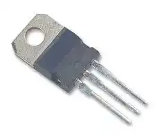
SCR THYRISTOR, 25A, 50V, TO-220AB
- Manufacturer: LITTELFUSE
- Product type: Thyristors - SCRs
- PEAK; SCR THYRISTOR, 25A, 50V, TO-220AB; Peak Repetitive Off-State Voltage, Vdrm:50V; Gate Trigger Current Max, Igt:30mA; Current It av:16A; On State RMS Current IT(rms):25A; Thyristor
- MSL: -
- SVHC: No SVHC (17-Dec-2014)
- No. of Pins: 3Pins
- Product Range: -
- Holding Current Max: 50mA
- On State RMS Current: 25A
- Thyristor Case Style: TO-220AB
- Average On State Current: 16A
- Gate Trigger Current Max: 30mA
- Gate Trigger Voltage Max: 1.5V
- Operating Temperature Max: 125°C
- Peak Non Repetitive Surge Current: 300A
- Peak Repetitive Off State Voltage: 50V
| Delivery and price | |
|---|---|
| Units per pack | 10000 |
| Price | 0.484 € |
| Current stock | 10+ |
| Lead time | 30 days |
## MCR69−2, MCR69−3 ## Silicon Controlled Rectifiers **Reverse Blocking Thyristors** Designed for overvoltage protection in crowbar circuits. ## **Features** - Glass-Passivated Junctions for Greater Parameter Stability and Reliability - Center-Gate Geometry for Uniform Current Spreading Enabling High Discharge Current - Small Rugged, Thermowatt Package Constructed for Low Thermal Resistance and Maximum Power Dissipation and Durability - High Capacitor Discharge Current, 750 Amps - Pb−Free Packages are Available* **MAXIMUM RATINGS** (TJ = 25°C unless otherwise noted) **Rating Symbol Value Unit** Peak Repetitive Off−State Voltage (Note 1) VDRM, V (TJ = 40 to +125°C, Gate Open) VRRM MCR69−2 50 MCR69−3 100 ~~ge~~ Peak Discharge Current (Note 2) ITM 750 A On-State RMS Current IT(RMS) 25 A (180° Conduction Angles; TC = 85°C) ~~ee~~ Average On-State Current IT(AV) 16 A (180° Conduction Angles; TC = 85°C) ~~ee~~ Peak Non-Repetitive Surge Current ITSM ~~ee~~ 300 A (1/2 Cycle, Sine Wave, 60 Hz, TJ = 125°C) ~~re~~ Circuit Fusing Considerations (t = 8.3 ms) I[2] t 375 A[2] s Forward Peak Gate Current IGM 2.0 A (t ≤ 1.0 s, TC = 85°C) Forward Peak Gate Power PGM 20 W (t ≤ 1.0 s, TC = 85°C) Forward Average Gate Power PG(AV) 0.5 W (t = 8.3 ms, TC = 85°C) ~~——~~ Operating Junction Temperature Range TJ −40 to +125 °C Storage Temperature Range Tstg −40 to +150 °C Mounting Torque − 8.0 in. lb. Maximum ratings are those values beyond which device damage can occur. Maximum ratings applied to the device are individual stress limit values (not normal operating conditions) and are not valid simultaneously. If these limits are exceeded, device functional operation is not implied, damage may occur and reliability may be affected. 1. VDRM and VRRM for all types can be applied on a continuous basis. Ratings apply for zero or negative gate voltage; however, positive gate voltage shall not be applied concurrent with negative potential on the anode. Blocking voltages shall not be tested with a constant current source such that the voltage ratings of the devices are exceeded. 2. Ratings apply for tw = 1 ms. See Figure 1 for ITM capability for various duration of an exponentially decaying current waveform, tw is defined as 5 time constants of an exponentially decaying current pulse. 3. Test Conditions: IG = 150 mA, VD = Rated VDRM, ITM = Rated Value, TJ = 125°C. - *For additional information on our Pb−Free strategy and soldering details, please download the ON Semiconductor Soldering and Mounting Techniques Reference Manual, SOLDERRM/D. ## **http://onsemi.com** **SCRs 25 AMPERES RMS 50 thru 100 VOLTS** **==> picture [172 x 217] intentionally omitted <==** **----- Start of picture text -----**<br> G<br>A K<br>MARKING<br>DIAGRAM<br>4<br>AYWW<br>TO−220AB MCR69x<br>CASE 221A AKA<br>STYLE 3<br>1 |<br>2<br>3<br>A = Assembly Location<br>Y = Year<br>WW = Work Week<br>MCR69 = Device Code<br>x = 2 or 3<br>AKA = Location Code<br>**----- End of picture text -----**<br> ## **PIN ASSIGNMENT** |1<br>2<br>3<br>4|Anode<br>Gate<br>Cathode<br>Anode| |---|---| ## **ORDERING INFORMATION** |**Device**|**Package**|**Shipping**†| |---|---|---| |MCR69−2|TO220AB|500/Box| |MCR69−2G|TO220AB<br>(Pb−Free)|500/Box| |MCR69−3|TO220AB|500/Box| |MCR69−3G|TO220AB<br>(Pb−Free)|500/Box| - †For information on tape and reel specifications, including part orientation and tape sizes, please refer to our Tape and Reel Packaging Specifications Brochure, BRD8011/D. Publication Order Number: **1** Semiconductor Components Industries, LLC, 2004 **December, 2004 − Rev. 1** **MCR69/D** **MCR69−2, MCR69−3** ## **THERMAL CHARACTERISTICS** |**THERMAL CHARACTERISTICS**|||| |---|---|---|---| |**Characteristic**|**Symbol**|**Max**|**Unit**| |Thermal Resistance, Junction−to−Case|R�JC|1.5|°C/W| |Thermal Resistance, Junction−to−Ambient|R�JA|60|°C/W| |Maximum Lead Temperature for Soldering Purposes 1/8 in from Case for 10 Seconds|TL|260|°C| |**ELECTRICAL CHARACTERISTICS** (TC= 25°C unless otherwise noted.)|**ELECTRICAL CHARACTERISTICS** (TC= 25°C unless otherwise noted.)|**ELECTRICAL CHARACTERISTICS** (TC= 25°C unless otherwise noted.)|**ELECTRICAL CHARACTERISTICS** (TC= 25°C unless otherwise noted.)|**ELECTRICAL CHARACTERISTICS** (TC= 25°C unless otherwise noted.)|**ELECTRICAL CHARACTERISTICS** (TC= 25°C unless otherwise noted.)| |---|---|---|---|---|---| |**Characteristic**|**Symbol**|**Min**|**Typ**|**Max**|**Unit**| |**OFF CHARACTERISTICS**|||||| |Peak Repetitive Forward or Reverse Blocking Current<br>(VAK= Rated VDRMor VRRM, Gate Open)<br>TJ= 25°C<br>TJ= 125°C|IDRM, IRRM|−<br>−|−<br>−|10<br>2.0|�A<br>mA| |**ON CHARACTERISTICS**|||||| |Peak Forward On-State Voltage<br>(ITM= 50 A) (Note 4)<br>(ITM= 750 A, tw= 1 ms) (Note 5)|VTM|−<br>−|−<br>6.0|1.8<br>−|V| |Gate Trigger Current (Continuous dc)<br>(VD= 12 V, RL= 100�)|IGT|2.0|7.0|30|mA| |Gate Trigger Voltage (Continuous dc)<br>(VD= 12 V, RL= 100�)|VGT|−|0.65|1.5|V| |Gate Non−Trigger Voltage<br>(VD= 12 Vdc, RL= 100�, TJ= 125°C)|VGD|0.2|0.40|−|V| |Holding Current<br>(VD= 12 V, Initiating Current = 200 mA, Gate Open)|IH|3.0|15|50|mA| |Latching Current<br>(VD= 12 Vdc, IG= 150 mA)|IL|−|−|60|mA| |Gate Controlled Turn-On Time (Note 6)<br>(VD= Rated VDRM, IG= 150 mA)<br>(ITM= 50 A Peak)|tgt|−|1.0|−|�s| |**DYNAMIC CHARACTERISTICS**|||||| |Critical Rate-of-Rise of Off-State Voltage<br>(VD= Rated VDRM, Gate Open, Exponential Waveform, TJ= 125°C)|dv/dt|10|−|−|V/�s| |Critical Rate-of-Rise of On-State Current<br>IG= 150 mA<br>TJ= 125°C|di/dt|−|−|100|A/�s| 4. Pulse duration � 300 � s, duty cycle � 2%. 5. Ratings apply for tw = 1 ms. See Figure 1 for ITM capability for various durations of an exponentially decaying current waveform. tw is defined as 5 time constants of an exponentially decaying current pulse. 6. The gate controlled turn-on time in a crowbar circuit will be influenced by the circuit inductance. **http://onsemi.com** **2** **MCR69−2, MCR69−3** ## **Voltage Current Characteristic of SCR** **==> picture [491 x 610] intentionally omitted <==** **----- Start of picture text -----**<br> + Current<br>Anode +<br>Symbol Parameter VTM<br>VDRM Peak Repetitive Off State Forward Voltage<br>on state<br>IDRM Peak Forward Blocking Current<br>VRRM Peak Repetitive Off State Reverse Voltage IRRM at VRRM IH<br>IRRM Peak Reverse Blocking Current<br>VTM Peak On State Voltage + Voltage<br>IH Holding Current Reverse Blocking Region IDRM at VDRM<br>(off state) Forward Blocking Region<br>(off state)<br>Reverse Avalanche Region<br>Anode −<br>1000<br>1.0<br>300<br>200 0.8<br>0.6<br>100<br>ITM<br>0.4<br>50<br>tw 0.2<br>20 tw = 5 time constants 0<br>0.5 1.0 2.0 5.0 10 20 50 25 50 75 100 125<br>tw, PULSE CURRENT DURATION (ms) TC, CASE TEMPERATURE ( ° C)<br>Figure 1. Peak Capacitor Discharge Current Figure 2. Peak Capacitor Discharge Current<br>Derating<br>125 32<br>120<br>Half Wave<br>115<br>24<br>110<br>dc<br>105<br>dc<br>100 16<br>95<br>90<br>Half Wave 8.0<br>85 TJ = 125 ° C<br>80<br>75 0<br>4.0 8.0 12 16 20 0 4.0 8.0 12 16 20<br>IT(AV), AVERAGE ON-STATE CURRENT (AMPS) IT(AV), AVERAGE ON-STATE CURRENT (AMPS)<br>NORMALIZED PEAK CURRENT<br>I , PEAK DISCHARGE CURRENT (AMPS)TM<br>°<br>CASE TEMPERATURE ( C)<br>(AV)<br>P , AVERAGE POWER DISSIPATION (WATTS)<br>C<br>T , MAXIMUM ALLOWABLE<br>**----- End of picture text -----**<br> **Figure 3. Current Derating** **Figure 4. Maximum Power Dissipation** **http://onsemi.com** **3** **MCR69−2, MCR69−3** **==> picture [513 x 624] intentionally omitted <==** **----- Start of picture text -----**<br> 1<br>0.7<br>0.5<br>0.3<br>0.2<br>Z�JC(t) = R�JC • r(t)<br>0.1<br>0.07<br>0.05<br>0.03<br>0.02<br>0.01<br>0.1 0.2 0.3 0.5 1 2 3 5 10 20 30 50 100 200 300 500 1 k 2 k 3 k 5 k 10 k<br>t, TIME (ms)<br>Figure 5. Thermal Response<br>10<br>1.4<br>5.0<br>VD = 12 Volts<br>3.0 RL = 100 � 1.2 VD = 12 Volts<br>2.0 RL = 100 �<br>1.0 1.0<br>0.5<br>0.8<br>0.3<br>0.2<br>0.5<br>−60 −40 −20 0 20 40 60 80 100 120 140 −60 −40 −20 0 20 40 60 80 100 120 140<br>TJ, JUNCTION TEMPERATURE ( ° C) TJ, JUNCTION TEMPERATURE ( ° C)<br>Figure 6. Gate Trigger Current Figure 7. Gate Trigger Voltage<br>3.0<br>2.0<br>VD = 12 Volts<br>ITM = 100 mA<br>1.0<br>0.8<br>0.5<br>0.3<br>−60 −40 −20 0 20 40 60 80 100 120 140<br>TJ, JUNCTION TEMPERATURE ( ° C)<br>r(t), TRANSIENT THERMAL RESISTANCE (NORMALIZED)<br>NORMALIZED GATE TRIGGER CURRENT NORMALIZED GATE TRIGGER VOLTAGE<br>NORMALIZED HOLD CURRENT<br>**----- End of picture text -----**<br> **Figure 8. Holding Current** **http://onsemi.com** **4** **MCR69−2, MCR69−3** ## **PACKAGE DIMENSIONS** ## **TO−220AB** CASE 221A−07 ISSUE AA **==> picture [242 x 168] intentionally omitted <==** **----- Start of picture text -----**<br> B F −T− SEATINGPLANE<br>C<br>4 T S<br>Q A<br>1 2 3<br>H<br>K U<br>Z<br>L<br>V<br>R<br>G<br>D J<br>N<br>**----- End of picture text -----**<br> - NOTES: 1. DIMENSIONING AND TOLERANCING PER ANSI Y14.5M, 1982. 2. CONTROLLING DIMENSION: INCH. |3.|DIME<br>BODY<br>ALLOW|SION Z DEFINES A ZONE WHERE AL<br>AND LEAD IRREGULARITIES ARE<br>ED.|SION Z DEFINES A ZONE WHERE AL<br>AND LEAD IRREGULARITIES ARE<br>ED.|SION Z DEFINES A ZONE WHERE AL<br>AND LEAD IRREGULARITIES ARE<br>ED.|SION Z DEFINES A ZONE WHERE AL<br>AND LEAD IRREGULARITIES ARE<br>ED.| |---|---|---|---|---|---| ||DIM|INCHES||MILLIMETERS|| |||MIN|MAX|MIN|MAX| ||A|0.570|0.620|14.48|15.75| ||B|0.380|0.405|9.66|10.28| ||C|0.160|0.190|4.07|4.82| ||D|0.025|0.035|0.64|0.88| ||F|0.142|0.147|3.61|3.73| ||G|0.095|0.105|2.42|2.66| ||H|0.110|0.155|2.80|3.93| ||J|0.014|0.022|0.36|0.55| ||K|0.500|0.562|12.70|14.27| ||L|0.045|0.060|1.15|1.52| ||N|0.190|0.210|4.83|5.33| ||Q|0.100|0.120|2.54|3.04| ||R|0.080|0.110|2.04|2.79| ||S|0.045|0.055|1.15|1.39| ||T|0.235|0.255|5.97|6.47| ||U|0.000|0.050|0.00|1.27| ||V|0.045|−−−|1.15|−−−| ||Z|−−−|0.080|−−−|2.04| ||STYL<br>PI|E 3:<br>N 1.<br>CATHODE<br>2.<br>ANODE<br>3.<br>GATE<br>4.<br>ANODE|||| **http://onsemi.com** **5** **MCR69−2, MCR69−3** **ON Semiconductor** and are registered trademarks of Semiconductor Components Industries, LLC (SCILLC). SCILLC reserves the right to make changes without further notice to any products herein. SCILLC makes no warranty, representation or guarantee regarding the suitability of its products for any particular purpose, nor does SCILLC assume any liability arising out of the application or use of any product or circuit, and specifically disclaims any and all liability, including without limitation special, consequential or incidental damages. “Typical” parameters which may be provided in SCILLC data sheets and/or specifications can and do vary in different applications and actual performance may vary over time. All operating parameters, including “Typicals” must be validated for each customer application by customer’s technical experts. SCILLC does not convey any license under its patent rights nor the rights of others. SCILLC products are not designed, intended, or authorized for use as components in systems intended for surgical implant into the body, or other applications intended to support or sustain life, or for any other application in which the failure of the SCILLC product could create a situation where personal injury or death may occur. Should Buyer purchase or use SCILLC products for any such unintended or unauthorized application, Buyer shall indemnify and hold SCILLC and its officers, employees, subsidiaries, affiliates, and distributors harmless against all claims, costs, damages, and expenses, and reasonable attorney fees arising out of, directly or indirectly, any claim of personal injury or death associated with such unintended or unauthorized use, even if such claim alleges that SCILLC was negligent regarding the design or manufacture of the part. SCILLC is an Equal Opportunity/Affirmative Action Employer. This literature is subject to all applicable copyright laws and is not for resale in any manner. ## **PUBLICATION ORDERING INFORMATION** **N. American Technical Support** : 800−282−9855 Toll Free USA/Canada **ON Semiconductor Website** : http://onsemi.com ## **LITERATURE FULFILLMENT** : Literature Distribution Center for ON Semiconductor USA/Canada P.O. Box 61312, Phoenix, Arizona 85082−1312 USA **Order Literature** : http://www.onsemi.com/litorder **Phone** : 480−829−7710 or 800−344−3860 Toll Free USA/Canada **Japan** : ON Semiconductor, Japan Customer Focus Center **Fax** : 480−829−7709 or 800−344−3867 Toll Free USA/Canada 2−9−1 Kamimeguro, Meguro−ku, Tokyo, Japan 153−0051 For additional information, please contact your **Email** : orderlit@onsemi.com **Phone** : 81−3−5773−3850 local Sales Representative. **MCR69/D** **http://onsemi.com** **6**
Updated at June 10, 2026
Founded in 1927 and headquartered in Chicago, Illinois, Littelfuse is a premier global manufacturer of circuit protection, power control, and sensing technologies. Widely recognized for pioneering the first small, fast-acting protective fuse, the company has grown into an industry leader whose highly reliable components are essential to modern industrial, transportation, and consumer electronics applications worldwide. At the core of the Littelfuse portfolio is an expansive and industry-leading range of circuit protection solutions. This encompasses a massive selection of traditional fuses, fuse holders, and resettable PTC thermistor fuses designed to safely interrupt overcurrent conditions. To defend against electrical overstress, Littelfuse also provides advanced transient voltage suppression (TVS) technologies, including thousands of specialized TVS diodes, TVS varistors, and gas discharge tubes (GDTs) that ensure robust defense against voltage spikes and environmental hazards. Beyond its foundational protection components, Littelfuse manufactures a diverse array of discrete semiconductors, sensors, and switching devices. Engineers rely on their high-performance thyristors, including TRIACs and SCRs, alongside power-efficient Schottky diodes and MOSFETs for demanding power control applications. Complemented by precision proximity sensors and highly reliable reed and solid-state relays, Littelfuse delivers the critical building blocks required for secure, efficient, and complete system design.
About Novapart
Novapart is a B2B electronic component broker specialising in stock shortages and cost reduction. We source hard-to-find parts and identify compliant alternatives across a catalogue of 420,000+ components from 500+ manufacturers.
Learn more →Stock Shortage Specialist
When a component is unavailable, discontinued or has an unacceptable lead time, we tap into our network of vetted European and Asian distributors to source what you need — without compromising on quality or traceability.
Request a quote →Compliant Alternatives
We identify pin-to-pin, electrically equivalent substitutes that meet the same certifications (RoHS, AEC-Q100, REACH) as your original specification — validated against datasheets, not just part numbers. Often at a lower cost.
BOM Analysis service →