
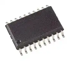


MCP23S08-E/SS
I/O Expander, 8bit, 10 MHz, Serial, SPI, 1.8 V, 5.5 V, SSOP
- Manufacturer: MICROCHIP
- Product type: I/O Expanders
- No. of Pins: 20Pins
- No. of I/O's: 16I/O's
- Bus Frequency: 10MHz
- IC Interface Type: Serial, SPI
- Chip Configuration: 8bit
- Supply Voltage Max: 5.5V
- Supply Voltage Min: 1.8V
- Interface Case Style: SSOP
| Delivery and price | |
|---|---|
| Units per pack | 100 |
| Price | 1.24 € |
| Current stock | 1000+ |
| Lead time | 7 days |
## **MCP23008/MCP23S08**

## **8-Bit I/O Expander with Serial Interface**

## **Features**

- 8-bit remote bidirectional I/O port

- I/O pins default to input

- High-speed I[2] C™ interface ( **MCP23008** )

- 100 kHz

- 400 kHz

- 1.7 MHz

- High-speed SPI interface ( **MCP23S08** ) - 10 MHz

- Hardware address pins

- Three for the MCP23008 to allow up to eight devices on the bus

- Two for the MCP23S08 to allow up to four devices using the same chip-select

- Configurable interrupt output pin

- Configurable as active-high, active-low or open-drain

- Configurable interrupt source

- Interrupt-on-change from configured defaults or pin change

- Polarity Inversion register to configure the polarity of the input port data

- External reset input

- Low standby current: 1 µA (max.)

- Operating voltage: - 1.8V to 5.5V @ -40°C to +85°C I[2] C @ 100 kHz SPI @ 5 MHz

- 2.7V to 5.5V @ -40°C to +85°C I[2] C @ 400 kHz SPI @ 10 MHz

- 4.5V to 5.5V @ -40°C to +125°C I[2] C @ 1.7 kHz SPI @ 10 MHz

## **Packages**

- 18-pin PDIP (300 mil)

- 18-pin SOIC (300 mil)

- 20-pin SSOP

- 20-pin QFN

## **Block Diagram**

**==> picture [410 x 241] intentionally omitted <==**

**----- Start of picture text -----**<br>
MCP23S08<br>SCK<br>SI<br>SO<br>MCP23008<br>SCL Serial Serializer/ GP0<br>SDA Interface  Deserializer 8 GP1<br>MCP23S08 GP2<br>3 GP3<br>A1:A0 A2:A0 Decode GPIO<br>GP4<br>Control<br>GP5<br>RESET<br>GP6<br>INT Interrupt GP7<br>Logic<br>8<br>VDD POR<br>Configuration/<br>Control<br>VSS Registers<br>**----- End of picture text -----**<br>


DS21919E-page 1

© 2007 Microchip Technology Inc.

**MCP23008/MCP23S08**

## **Package Types**

**==> picture [385 x 436] intentionally omitted <==**

**----- Start of picture text -----**<br>
MCP23008<br>PDIP/SOIC SSOP<br>SCL 1 18 VDD SCL 1 20 VDD<br>SDA 2 17 GP7 SDA 2 19 GP7<br>A2 3 16 GP6 A2 3 18 GP6<br>A1 4 17 GP5<br>A1 4 15 GP5<br>A0 5 16 GP4<br>A0 5 14 GP4<br>RESET 6 15 GP3<br>RESET 6 13 GP3 NC 7 14 GP2<br>NC 7 12 GP2 INT 8 13 GP1<br>INT 8 11 GP1 VSS 9 12 GP0<br>VSS 9 10 GP0 N/C 1 0 11 N/C<br>QFN<br>A2 1 15 GP6<br>A1 2 14 GP5<br>A0 3 MCP23008 13 GP4<br>RESET 4 12 GP3<br>NC 5 11 GP2<br>MCP23008<br>MCP23008<br>DD SS<br>SDA SCL V V GP7<br>20 19 18 17 16<br>6 7 8 9 10<br>N/C INT N/C GP0 GP1<br>**----- End of picture text -----**<br>


DS21919E-page 2

© 2007 Microchip Technology Inc.

**MCP23008/MCP23S08**

## **Package Types: (Continued)**

|SI<br>SCK<br>A1<br><br>SO|||1<br>2<br>3<br>4<br>5<br>6<br>7<br>18<br>17<br>16<br>15<br>14<br>13<br>12<br>**PDIP/SOIC**<br>8<br>9<br>11<br>10<br>**MCP23S08**<br>A0<br>A1<br>RESET<br>A2<br>CS|GP4<br>VDD<br>GP7<br>GP6<br>GP5<br>GP3<br>GP2<br>GP1<br>GP0<br>**MCP23S08**<br>SI<br>SCK<br>VSS<br>A0<br>N/C<br>A1<br>RESET<br>SO<br>CS<br>INT<br>**QFN**<br>**MCP23S08**<br>20<br>19<br>18<br>17<br>16<br>6<br>7<br>8<br>9<br>10<br>15<br>14<br>13<br>12<br>11<br>1<br>2<br>3<br>4<br>5<br>SCK<br>SI<br>VSS<br>N/C<br>INT<br>VDD<br>GP7<br>GP1<br>GP0<br>N/C||**MCP23S08**<br>13<br>12<br>1<br>2<br>3<br>4<br>5<br>6<br>7<br>8<br>9<br>20<br>19<br>18<br>17<br>16<br>15<br>14<br>11<br>~~1~~0<br>GP3<br>VDD<br>GP7<br>GP6<br>GP5<br>GP2<br>GP1<br>GP0<br>N/C<br>GP4<br> **SSOP**<br>GP3<br>GP6<br>GP5<br>GP2<br>GP4|
|---|---|---|---|---|---|---|
||||1<br>2<br>3<br>4<br><br>18<br>17<br>16<br>15<br><br>**3S08**||||
|CS<br>INT<br>RESET<br>A0<br>VSS|||5<br>6<br>7<br>14<br>13<br>12<br>8<br>9<br>11<br>10<br>**MCP2**||||
||||||||
||||||||
||||||||
||||||||
||||||||
||||||||


DS21919E-page 3

© 2007 Microchip Technology Inc.

**MCP23008/MCP23S08**

## **NOTES:**

DS21919E-page 4

© 2007 Microchip Technology Inc.

**MCP23008/MCP23S08**

## **1.0 DEVICE OVERVIEW**

The MCP23X08 device provides 8-bit, general purpose, parallel I/O expansion for I[2] C bus or SPI applications. The two devices differ in the number of hardware address pins and the serial interface:

- MCP23008 – I[2] C interface; three address pins

- MCP23S08 – SPI interface; two address pins

The MCP23X08 consists of multiple 8-bit configuration registers for input, output and polarity selection. The system master can enable the I/Os as either inputs or outputs by writing the I/O configuration bits. The data for each input or output is kept in the corresponding Input or Output register. The polarity of the Input Port register can be inverted with the Polarity Inversion register. All registers can be read by the system master.

The interrupt output can be configured to activate under two conditions (mutually exclusive):

1. When any input state differs from its corresponding input port register state, this is used to indicate to the system master that an input state has changed.

2. When an input state differs from a preconfigured register value (DEFVAL register).

The Interrupt Capture register captures port values at the time of the interrupt, thereby saving the condition that caused the interrupt.

The Power-on Reset (POR) sets the registers to their default values and initializes the device state machine.

The hardware address pins are used to determine the device address.

## **1.1 Pin Descriptions**

**TABLE 1-1: PINOUT DESCRIPTION**

|**Pin**<br>**Name**|**PDIP/**<br>**SOIC**|**QFN**|**SSOP**|**Pin**<br>**Type**|**Function**|
|---|---|---|---|---|---|
|SCL/SCK|1|19|1|I|Serial clock input.|
|SDA/SI|2|20|2|I/O|Serial data I/O(**MCP23008**)/Serial data input(**MCP23S08**).|
|A2/SO|3|1|3|I/O|Hardware address input (**MCP23008**)/<br>Serial data output (**MCP23S08**).<br>A2 must be biased externally.|
|A1|4|2|4|I|Hardware address input. Must be biased externally.|
|A0|5|3|5|I|Hardware address input. Must be biased externally.|
|RESET|6|4|6|I|External reset input. Must be biased externally.|
|NC/CS|7|5|7|I|No connect(**MCP23008**)/External chipselect input(**MCP23S08**).|
|INT|8|7|8|O|Interrupt output. Can be configured for active-high, active-low or<br>open-drain.|
|VSS|9|17|9|P|Ground.|
|GP0|10|9|12|I/O|Bidirectional I/O pin. Can be enabled for interrupt-on-change and/or<br>internal weakpull-upresistor.|
|GP1|11|10|13|I/O|Bidirectional I/O pin. Can be enabled for interrupt-on-change and/or<br>internal weakpull-upresistor.|
|GP2|12|11|14|I/O|Bidirectional I/O pin. Can be enabled for interrupt-on-change and/or<br>internal weakpull-upresistor.|
|GP3|13|12|15|I/O|Bidirectional I/O pin. Can be enabled for interrupt-on-change and/or<br>internal weakpull-upresistor.|
|GP4|14|13|16|I/O|Bidirectional I/O pin. Can be enabled for interrupt-on-change and/or<br>internal weakpull-upresistor.|
|GP5|15|14|17|I/O|Bidirectional I/O pin. Can be enabled for interrupt-on-change and/or<br>internal weakpull-upresistor.|
|GP6|16|15|18|I/O|Bidirectional I/O pin. Can be enabled for interrupt-on-change and/or<br>internal weakpull-upresistor.|
|GP7|17|16|19|I/O|Bidirectional I/O pin. Can be enabled for interrupt-on-change and/or<br>internal weakpull-upresistor.|
|VDD|18|18|20|P|Power.|
|N/C|—|6, 8|10, 11|—|—|


DS21919E-page 5

© 2007 Microchip Technology Inc.

## **MCP23008/MCP23S08**

## **1.2 Power-on Reset (POR)**

The on-chip POR circuit holds the device in reset until VDD has reached a high enough voltage to deactivate the POR circuit (i.e., release the device from Reset). The maximum VDD rise time is specified in **Section 2.0 “Electrical Characteristics”** .

When the device exits the POR condition (releases reset), device operating parameters (i.e., voltage, temperature, serial bus frequency, etc.) must be met to ensure proper operation.

## **1.3 Serial Interface**

This block handles the functionality of the I[2] C (MCP23008) or SPI (MCP23S08) interface protocol. The MCP23X08 contains eleven registers that can be addressed through the serial interface block (Table 1-2):

**TABLE 1-2: REGISTER ADDRESSES**

|**Address**|**Access to:**|
|---|---|
|00h|IODIR|
|01h|IPOL|
|02h|GPINTEN|
|03h|DEFVAL|
|04h|INTCON|
|05h|IOCON|
|06h|GPPU|
|07h|INTF|
|08h|INTCAP(Read-only)|
|09h|GPIO|
|0Ah|OLAT|


## 1.3.1 SEQUENTIAL OPERATION BIT

The Sequential Operation (SEQOP) bit (IOCON register) controls the operation of the address pointer. The address pointer can either be enabled (default) to allow the address pointer to increment automatically after each data transfer, or it can be disabled.

When operating in **Sequential mode** (IOCON.SEQOP = 0 ), the address pointer automatically increments to the next address after each byte is clocked.

When operating in **Byte mode** (IOCON.SEQOP = 1 ), the MCP23X08 does not increment its address counter after each byte during the data transfer. This gives the ability to continually read the same address by providing extra clocks (without additional control bytes). This is useful for polling the GPIO register for data changes.

## 1.3.2 I[2] C™ INTERFACE

## 1.3.2.1 I[2] C Write Operation

The I[2] C Write operation includes the control byte and register address sequence, as shown in the bottom of Figure 1-1. This sequence is followed by eight bits of data from the master and an Acknowledge (ACK) from the MCP23008. The operation is ended with a STOP or RESTART condition being generated by the master.

Data is written to the MCP23008 after every byte transfer. If a STOP or RESTART condition is generated during a data transfer, the data will not be written to the MCP23008.

Byte writes and sequential writes are both supported by the MCP23008. The MCP23008 increments its address counter after each ACK during the data transfer.

## 1.3.2.2 I[2] C Read Operation

The I[2] C Read operation includes the control byte sequence, as shown in the bottom of Figure 1-1. This sequence is followed by another control byte (including the START condition and ACK) with the R/W bit equal to a logic 1 (R/W = 1 ). The MCP23008 then transmits the data contained in the addressed register. The sequence is ended with the master generating a STOP or RESTART condition.

## 1.3.2.3 I[2] C Sequential Write/Read

For sequential operations (Write or Read), instead of transmitting a STOP or RESTART condition after the data transfer, the master clocks the next byte pointed to by the address pointer (see **Section 1.3.1 “Sequential Operation Bit”** for details regarding sequential operation control).

The sequence ends with the master sending a STOP or RESTART condition.

The MCP23008 address pointer will roll over to address zero after reaching the last register address. Refer to Figure 1-1.

## 1.3.3 SPI INTERFACE

## 1.3.3.1 SPI Write Operation

The SPI Write operation is started by lowering CS. The Write command (slave address with R/W bit cleared) is then clocked into the device. The opcode is followed by an address and at least one data byte.

## 1.3.3.2 SPI Read Operation

The SPI Read operation is started by lowering CS. The SPI read command (slave address with R/W bit set) is then clocked into the device. The opcode is followed by an address, with at least one data byte being clocked out of the device.

DS21919E-page 6

© 2007 Microchip Technology Inc.

**MCP23008/MCP23S08**

## **FIGURE 1-1: MCP23008 I[2] C™ DEVICE PROTOCOL**

**==> picture [468 x 477] intentionally omitted <==**

**----- Start of picture text -----**<br>
S - START<br>SR - RESTART<br>S OP W ADDR DIN .... DIN P<br>P - STOP<br>w - Write SR OP R DOUT .... DOUT P<br>R - Read<br>OP - Device opcode SR OP W DIN .... DIN P<br>ADDR - Device address<br>P<br>DOUT - Data out from  MCP23008<br>DIN - Data into  MCP23008<br>S OP R DOUT .... DOUT P<br>SR OP R DOUT .... DOUT P<br>SR OP W ADDR DIN .... DIN P<br>P<br>Byte and Sequential Write<br>Byte S OP W ADDR DIN P<br>Sequential S OP W ADDR DIN .... DIN P<br>Byte and Sequential Read<br>Byte S OP W SR OP R DOUT P<br>Sequential S OP W SR OP R DOUT .... DOUT P<br>**----- End of picture text -----**<br>


## 1.3.3.3 SPI Sequential Write/Read

For sequential operations, instead of deselecting the device by raising CS, the master clocks the next byte pointed to by the address pointer.

The sequence ends by the raising of CS.

The MCP23S08 address pointer will roll over to address zero after reaching the last register address.

## **1.4 Hardware Address Decoder**

The hardware address pins are used to determine the device address. To address a device, the corresponding address bits in the control byte must match the pin state.

- MCP23008 has address pins A2, A1 and A0.

- MCP23S08 has address pins A1 and A0.

The pins must be biased externally.

DS21919E-page 7

© 2007 Microchip Technology Inc.

## **MCP23008/MCP23S08**

## 1.4.1 ADDRESSING I[2] C DEVICES (MCP23008)

The MCP23008 is a slave I[2] C device that supports 7-bit slave addressing, with the read/write bit filling out the control byte. The slave address contains four fixed bits and three user-defined hardware address bits (pins A2, A1 and A0). Figure 1-2 shows the control byte format.

## 1.4.2 ADDRESSING SPI DEVICES (MCP23S08)

The MCP23S08 is a slave SPI device. The slave address contains five fixed bits and two user-defined hardware address bits (pins A1 and A0), with the read/ write bit filling out the control byte. Figure 1-3 shows the control byte format.

## **FIGURE 1-2: I[2] C™ CONTROL BYTE FORMAT**

**==> picture [213 x 96] intentionally omitted <==**

**----- Start of picture text -----**<br>
Control Byte<br>S 0 1 0 0 A2 A1 A0 R/W ACK<br>Slave Address<br>Start R/W bit<br>bit ACK bit<br>R/W =  0  = write<br>R/W =  1  = read<br>**----- End of picture text -----**<br>


## **FIGURE 1-3: SPI CONTROL BYTE FORMAT**

**==> picture [205 x 111] intentionally omitted <==**

**----- Start of picture text -----**<br>
CS<br>Control Byte<br>0 1 0 0 0 A1 A0 R/W<br>Slave Address<br>R/W bit<br>R/W =  0  = write<br>R/W =  1  = read<br>**----- End of picture text -----**<br>


## **FIGURE 1-4:**

## **I[2] C™ ADDRESSING REGISTERS**

**==> picture [444 x 96] intentionally omitted <==**

**----- Start of picture text -----**<br>
S 0 1 0 0 A2 A1 A0 0 ACK A7 A6 A5 A4 A3 A2 A1 A0 ACK<br>R/W = 0<br>Device Opcode Register Address<br>The ACKs are provided by the MCP23008.<br>**----- End of picture text -----**<br>


## **FIGURE 1-5:**

## **SPI ADDRESSING REGISTERS**

**==> picture [450 x 65] intentionally omitted <==**

**----- Start of picture text -----**<br>
CS<br>0 1 0 0 0 A1 A0 R/W A7 A6 A5 A4 A3 A2 A1 A0<br>Device Opcode Register Address<br>**----- End of picture text -----**<br>


DS21919E-page 8

© 2007 Microchip Technology Inc.

**MCP23008/MCP23S08**

## **1.5 GPIO Port**

The GPIO module contains the data port (GPIO), internal pull up resistors and the Output Latches (OLAT).

## **1.6 Configuration and Control Registers**

The Configuration and Control blocks contain the registers as shown in Table 1-3.

Reading the GPIO register reads the value on the port. Reading the OLAT register only reads the OLAT, not the actual value on the port.

Writing to the GPIO register actually causes a write to the OLAT. Writing to the OLAT register forces the associated output drivers to drive to the level in OLAT. Pins configured as inputs turn off the associated output driver and put it in high-impedance.

## **TABLE 1-3: CONFIGURATION AND CONTROL REGISTERS**

|**Register**<br>**Name**|**Address**<br>**(hex)**|**bit 7**|**bit 6**|**bit 5**|**bit 4**|**bit 3**|**bit 2**|**bit 1**|**bit 0**|**POR/RST**<br>**value**|
|---|---|---|---|---|---|---|---|---|---|---|
|IODIR|00|IO7|IO6|IO5|IO4|IO3|IO2|IO1|IO0|1111 1111|
|IPOL|01|IP7|IP6|IP5|IP4|IP3|IP2|IP1|IP0|0000 0000|
|GPINTEN|02|GPINT7|GPINT6|GPINT5|GPINT4|GPINT3|GPINT2|GPINT1|GPINT0|0000 0000|
|DEFVAL|03|DEF7|DEF6|DEF5|DEF4|DEF3|DEF2|DEF1|DEF0|0000 0000|
|INTCON|04|IOC7|IOC6|IOC5|IOC4|IOC3|IOC2|IOC1|IOC0|0000 0000|
|IOCON|05|—|—|SREAD|DISSLW|HAEN*****|ODR|INTPOL|—|--00 000-|
|GPPU|06|PU7|PU6|PU5|PU4|PU3|PU2|PU1|PU0|0000 0000|
|INTF|07|INT7|INT6|INT5|INT4|INT3|INT2|INT1|INTO|0000 0000|
|INTCAP|08|ICP7|ICP6|ICP5|ICP4|ICP3|ICP2|ICP1|ICP0|0000 0000|
|GPIO|09|GP7|GP6|GP5|GP4|GP3|GP2|GP1|GP0|0000 0000|
|OLAT|0A|OL7|OL6|OL5|OL4|OL3|OL2|OL1|OL0|0000 0000|


***** Not used on the MCP23008.

DS21919E-page 9

© 2007 Microchip Technology Inc.

## **MCP23008/MCP23S08**

## 1.6.1 I/O DIRECTION (IODIR) REGISTER

Controls the direction of the data I/O.

When a bit is set, the corresponding pin becomes an input. When a bit is clear, the corresponding pin becomes an output.

## **REGISTER 1-1:**

## **IODIR – I/O DIRECTION REGISTER (ADDR 0x00)**

|**REGISTER 1-1:**<br>**IODIR – I/O DIRECTION REGISTER (ADDR 0x00)**|**REGISTER 1-1:**<br>**IODIR – I/O DIRECTION REGISTER (ADDR 0x00)**|**REGISTER 1-1:**<br>**IODIR – I/O DIRECTION REGISTER (ADDR 0x00)**|**REGISTER 1-1:**<br>**IODIR – I/O DIRECTION REGISTER (ADDR 0x00)**|**REGISTER 1-1:**<br>**IODIR – I/O DIRECTION REGISTER (ADDR 0x00)**|**REGISTER 1-1:**<br>**IODIR – I/O DIRECTION REGISTER (ADDR 0x00)**|**REGISTER 1-1:**<br>**IODIR – I/O DIRECTION REGISTER (ADDR 0x00)**|**REGISTER 1-1:**<br>**IODIR – I/O DIRECTION REGISTER (ADDR 0x00)**|
|---|---|---|---|---|---|---|---|
|||||||||
|R/W-1<br>R/W-1<br>R/W-1<br>R/W-1<br>R/W-1<br>R/W-1<br>R/W-1<br>R/W-1||||||||
|IO7|IO6|IO5|IO4|IO3|IO2|IO1|IO0|
|bit 7<br>bit 0||||||||
|||||||||
|**Legend:**<br>R = Readable bit<br>W = Writable bit<br>U = Unimplemented bit, read as ‘0’<br>-n = Value at POR<br>‘1’ = Bit is set<br>‘0’ = Bit is cleared<br>x = Bit is unknown||||||||
|||||||||


bit 7-0 **IO7:IO0:** These bits control the direction of data I/O <7:0>

1 = Pin is configured as an input.

0 = Pin is configured as an output.

DS21919E-page 10

© 2007 Microchip Technology Inc.

**MCP23008/MCP23S08**

## 1.6.2 INPUT POLARITY (IPOL) REGISTER

The IPOL register allows the user to configure the polarity on the corresponding GPIO port bits.

If a bit is set, the corresponding GPIO register bit will reflect the inverted value on the pin.

## **REGISTER 1-2:**

## **IPOL – INPUT POLARITY PORT REGISTER (ADDR 0x01)**

|**REGISTER 1-2:**<br>**IPOL – INPUT POLARITY PORT REGISTER (ADDR 0x01)**|**REGISTER 1-2:**<br>**IPOL – INPUT POLARITY PORT REGISTER (ADDR 0x01)**|**REGISTER 1-2:**<br>**IPOL – INPUT POLARITY PORT REGISTER (ADDR 0x01)**|**REGISTER 1-2:**<br>**IPOL – INPUT POLARITY PORT REGISTER (ADDR 0x01)**|**REGISTER 1-2:**<br>**IPOL – INPUT POLARITY PORT REGISTER (ADDR 0x01)**|**REGISTER 1-2:**<br>**IPOL – INPUT POLARITY PORT REGISTER (ADDR 0x01)**|**REGISTER 1-2:**<br>**IPOL – INPUT POLARITY PORT REGISTER (ADDR 0x01)**|**REGISTER 1-2:**<br>**IPOL – INPUT POLARITY PORT REGISTER (ADDR 0x01)**|
|---|---|---|---|---|---|---|---|
|||||||||
|R/W-0<br>R/W-0<br>R/W-0<br>R/W-0<br>R/W-0<br>R/W-0<br>R/W-0<br>R/W-0||||||||
|IP7|IP6|IP5|IP4|IP3|IP2|IP1|IP0|
|bit 7<br>bit 0||||||||


## **Legend:**

|**Legend:**|||
|---|---|---|
|R = Readable bit|W = Writable bit|U = Unimplemented bit, read as ‘0’|
|-n = Value at POR|‘1’ = Bit is set|‘0’ = Bit is cleared<br>x = Bit is unknown|


bit 7-0 **IP7:IP0:** These bits control the polarity inversion of the input pins <7:0>

1 = GPIO register bit will reflect the opposite logic state of the input pin.

0 = GPIO register bit will reflect the same logic state of the input pin.

DS21919E-page 11

© 2007 Microchip Technology Inc.

**MCP23008/MCP23S08**

## 1.6.3 INTERRUPT-ON-CHANGE CONTROL (GPINTEN) REGISTER

The GPINTEN register controls the interrupt-onchange feature for each pin.

If a bit is set, the corresponding pin is enabled for interrupt-on-change. The DEFVAL and INTCON registers must also be configured if any pins are enabled for interrupt-on-change.

## **REGISTER 1-3:**

**GPINTEN – INTERRUPT-ON-CHANGE PINS (ADDR 0x02)**

|**REGISTER 1-3:**<br>**GPINTEN – INTERRUPT-ON-CHANGE PINS (ADDR 0x02)**|**REGISTER 1-3:**<br>**GPINTEN – INTERRUPT-ON-CHANGE PINS (ADDR 0x02)**|**REGISTER 1-3:**<br>**GPINTEN – INTERRUPT-ON-CHANGE PINS (ADDR 0x02)**|**REGISTER 1-3:**<br>**GPINTEN – INTERRUPT-ON-CHANGE PINS (ADDR 0x02)**|**REGISTER 1-3:**<br>**GPINTEN – INTERRUPT-ON-CHANGE PINS (ADDR 0x02)**|**REGISTER 1-3:**<br>**GPINTEN – INTERRUPT-ON-CHANGE PINS (ADDR 0x02)**|**REGISTER 1-3:**<br>**GPINTEN – INTERRUPT-ON-CHANGE PINS (ADDR 0x02)**|**REGISTER 1-3:**<br>**GPINTEN – INTERRUPT-ON-CHANGE PINS (ADDR 0x02)**|
|---|---|---|---|---|---|---|---|
|R/W-0<br>R/W-0<br>R/W-0<br>R/W-0<br>R/W-0<br>R/W-0<br>R/W-0<br>R/W-0||||||||
|GPINT7|GPINT6|GPINT5|GPINT4|GPINT3|GPINT2|GPINT1|GPINT0|
|bit 7<br>bit 0||||||||
|||||||||
|**Legend:**<br>R = Readable bit<br>W = Writable bit<br>U = Unimplemented bit, read as ‘0’<br>-n = Value at POR<br>‘1’ = Bit is set<br>‘0’ = Bit is cleared<br>x = Bit is unknown||||||||


bit 7-0 **GPINT7:GPINT0:** General purpose I/O interrupt-on-change bits <7:0>

- 1 = Enable GPIO input pin for interrupt-on-change event.

- 0 = Disable GPIO input pin for interrupt-on-change event.

Refer to INTCON and GPINTEN.

DS21919E-page 12

© 2007 Microchip Technology Inc.

**MCP23008/MCP23S08**

## 1.6.4 DEFAULT COMPARE (DEFVAL) REGISTER FOR INTERRUPT-ONCHANGE

The default comparison value is configured in the DEFVAL register. If enabled (via GPINTEN and INTCON) to compare against the DEFVAL register, an opposite value on the associated pin will cause an interrupt to occur.

## **REGISTER 1-4: DEFVAL – DEFAULT VALUE REGISTER (ADDR 0x03)**

|**REGISTER 1-4:**<br>**DEFVAL – DEFAULT VALUE REGISTER (ADDR 0x03)**|**REGISTER 1-4:**<br>**DEFVAL – DEFAULT VALUE REGISTER (ADDR 0x03)**|**REGISTER 1-4:**<br>**DEFVAL – DEFAULT VALUE REGISTER (ADDR 0x03)**|**REGISTER 1-4:**<br>**DEFVAL – DEFAULT VALUE REGISTER (ADDR 0x03)**|**REGISTER 1-4:**<br>**DEFVAL – DEFAULT VALUE REGISTER (ADDR 0x03)**|**REGISTER 1-4:**<br>**DEFVAL – DEFAULT VALUE REGISTER (ADDR 0x03)**|**REGISTER 1-4:**<br>**DEFVAL – DEFAULT VALUE REGISTER (ADDR 0x03)**|**REGISTER 1-4:**<br>**DEFVAL – DEFAULT VALUE REGISTER (ADDR 0x03)**|
|---|---|---|---|---|---|---|---|
|R/W-0<br>R/W-0<br>R/W-0<br>R/W-0<br>R/W-0<br>R/W-0<br>R/W-0<br>R/W-0||||||||
|DEF7|DEF6|DEF5|DEF4|DEF3|DEF2|DEF1|DEF0|
|bit 7<br>bit 0||||||||
|||||||||
|**Legend:**<br>R = Readable bit<br>W = Writable bit<br>U = Unimplemented bit, read as ‘0’<br>-n = Value at POR<br>‘1’ = Bit is set<br>‘0’ = Bit is cleared<br>x = Bit is unknown||||||||


bit 7-0 **DEF7:DEF0:** These bits set the compare value for pins configured for interrupt-on-change from defaults <7:0>. Refer to INTCON.

If the associated pin level is the opposite from the register bit, an interrupt occurs.

Refer to INTCON and GPINTEN.

DS21919E-page 13

© 2007 Microchip Technology Inc.

**MCP23008/MCP23S08**

## 1.6.5 INTERRUPT CONTROL (INTCON) REGISTER

The INTCON register controls how the associated pin value is compared for the interrupt-on-change feature. If a bit is set, the corresponding I/O pin is compared against the associated bit in the DEFVAL register. If a bit value is clear, the corresponding I/O pin is compared against the previous value.

## **REGISTER 1-5:**

**INTCON – INTERRUPT-ON-CHANGE CONTROL REGISTER (ADDR 0x04)**

|**REGISTER 1-5:**<br>**INTCON – INTERRUPT-ON-CHANGE CONTROL REGISTER (ADDR 0x04)**|**REGISTER 1-5:**<br>**INTCON – INTERRUPT-ON-CHANGE CONTROL REGISTER (ADDR 0x04)**|**REGISTER 1-5:**<br>**INTCON – INTERRUPT-ON-CHANGE CONTROL REGISTER (ADDR 0x04)**|**REGISTER 1-5:**<br>**INTCON – INTERRUPT-ON-CHANGE CONTROL REGISTER (ADDR 0x04)**|**REGISTER 1-5:**<br>**INTCON – INTERRUPT-ON-CHANGE CONTROL REGISTER (ADDR 0x04)**|**REGISTER 1-5:**<br>**INTCON – INTERRUPT-ON-CHANGE CONTROL REGISTER (ADDR 0x04)**|**REGISTER 1-5:**<br>**INTCON – INTERRUPT-ON-CHANGE CONTROL REGISTER (ADDR 0x04)**|**REGISTER 1-5:**<br>**INTCON – INTERRUPT-ON-CHANGE CONTROL REGISTER (ADDR 0x04)**|
|---|---|---|---|---|---|---|---|
|||||||||
|R/W-0<br>R/W-0<br>R/W-0<br>R/W-0<br>R/W-0<br>R/W-0<br>R/W-0<br>R/W-0||||||||
|IOC7|IOC6|IOC5|IOC4|IOC3|IOC2|IOC1|IOC0|
|bit 7<br>bit 0||||||||
|||||||||
|**Legend:**<br>R = Readable bit<br>W = Writable bit<br>U = Unimplemented bit, read as ‘0’<br>-n = Value at POR<br>‘1’ = Bit is set<br>‘0’ = Bit is cleared<br>x = Bit is unknown||||||||
|||||||||


bit 7-0 **IOC7:IOC0:** These bits control how the associated pin value is compared for interrupt-on-change <7:0>

1 = Controls how the associated pin value is compared for interrupt-on-change.

- 0 = Pin value is compared against the previous pin value.

Refer to INTCON and GPINTEN.

DS21919E-page 14

© 2007 Microchip Technology Inc.

**MCP23008/MCP23S08**

## 1.6.6 CONFIGURATION (IOCON) REGISTER

The IOCON register contains several bits for configuring the device:

- The Sequential Operation (SEQOP) controls the incrementing function of the address pointer. If the address pointer is disabled, the address pointer does not automatically increment after each byte is clocked during a serial transfer. This feature is useful when it is desired to continuously poll (read) or modify (write) a register.

   - The Hardware Address Enable (HAEN) control bit enables/disables the hardware address pins (A1, A0) on the MCP23S08. This bit is not used on the MCP23008. The address pins are always enabled on the MCP23008.

   - The Open-Drain (ODR) control bit enables/ disables the INT pin for open-drain configuration.

   - The Interrupt Polarity (INTPOL) control bit sets the polarity of the INT pin. This bit is functional only when the ODR bit is cleared, configuring the INT pin as active push-pull.

- The Slew Rate (DISSLW) bit controls the slew rate function on the SDA pin. If enabled, the SDA slew rate will be controlled when driving from a high to a low.

## **REGISTER 1-6:**

**IOCON – I/O EXPANDER CONFIGURATION REGISTER (ADDR 0x05)**

|**REGISTER 1-6:**<br>**IOCON – I/O EXPANDER CONFIGURATION REGISTER (ADDR 0x05)**|**REGISTER 1-6:**<br>**IOCON – I/O EXPANDER CONFIGURATION REGISTER (ADDR 0x05)**|**REGISTER 1-6:**<br>**IOCON – I/O EXPANDER CONFIGURATION REGISTER (ADDR 0x05)**|**REGISTER 1-6:**<br>**IOCON – I/O EXPANDER CONFIGURATION REGISTER (ADDR 0x05)**|**REGISTER 1-6:**<br>**IOCON – I/O EXPANDER CONFIGURATION REGISTER (ADDR 0x05)**|**REGISTER 1-6:**<br>**IOCON – I/O EXPANDER CONFIGURATION REGISTER (ADDR 0x05)**|**REGISTER 1-6:**<br>**IOCON – I/O EXPANDER CONFIGURATION REGISTER (ADDR 0x05)**|**REGISTER 1-6:**<br>**IOCON – I/O EXPANDER CONFIGURATION REGISTER (ADDR 0x05)**|
|---|---|---|---|---|---|---|---|
|U-0<br>U-0<br>R/W-0<br>R/W-0<br>R/W-0<br>R/W-0<br>R/W-0<br>U-0||||||||
|—|—|SEQOP|DISSLW|HAEN|ODR|INTPOL|—|
|bit 7<br>bit 0||||||||
|||||||||
|**Legend:**<br>R = Readable bit<br>W = Writable bit<br>U = Unimplemented bit, read as ‘0’<br>-n = Value at POR<br>‘1’ = Bit is set<br>‘0’ = Bit is cleared<br>x = Bit is unknown||||||||


bit 7-6 **Unimplemented:** Read as ‘ 0 ’.

- bit 5 **SEQOP:** Sequential Operation mode bit.

- 1 = Sequential operation disabled, address pointer does not increment. 0 =  Sequential operation enabled, address pointer increments.

- bit 4 **DISSLW:** Slew Rate control bit for SDA output.

   - 1 = Slew rate disabled.

   - 0 =  Slew rate enabled.

- bit 3 **HAEN:** Hardware Address Enable bit (MCP23S08 only). Address pins are always enabled on MCP23008.

   - 1 = Enables the MCP23S08 address pins.

   - 0 =  Disables the MCP23S08 address pins.

- bit 2 **ODR:** This bit configures the INT pin as an open-drain output.

- 1 = Open-drain output (overrides the INTPOL bit). 0 =  Active driver output (INTPOL bit sets the polarity).

- bit 1 **INTPOL:** This bit sets the polarity of the INT output pin.

   - 1 = Active-high. 0 =  Active-low.

- bit 0 **Unimplemented:** Read as ‘ 0 ’.

DS21919E-page 15

© 2007 Microchip Technology Inc.

## **MCP23008/MCP23S08**

## 1.6.7 PULL-UP RESISTOR CONFIGURATION (GPPU) REGISTER

The GPPU register controls the pull-up resistors for the port pins. If a bit is set and the corresponding pin is configured as an input, the corresponding port pin is internally pulled up with a 100 kΩ resistor.

## **REGISTER 1-7: GPPU – GPIO PULL-UP RESISTOR REGISTER (ADDR 0x06)**

|**REGISTER 1-7:**<br>**GPPU – GPIO PULL-UP RESISTOR REGISTER (ADDR 0x06)**|**REGISTER 1-7:**<br>**GPPU – GPIO PULL-UP RESISTOR REGISTER (ADDR 0x06)**|**REGISTER 1-7:**<br>**GPPU – GPIO PULL-UP RESISTOR REGISTER (ADDR 0x06)**|**REGISTER 1-7:**<br>**GPPU – GPIO PULL-UP RESISTOR REGISTER (ADDR 0x06)**|**REGISTER 1-7:**<br>**GPPU – GPIO PULL-UP RESISTOR REGISTER (ADDR 0x06)**|**REGISTER 1-7:**<br>**GPPU – GPIO PULL-UP RESISTOR REGISTER (ADDR 0x06)**|**REGISTER 1-7:**<br>**GPPU – GPIO PULL-UP RESISTOR REGISTER (ADDR 0x06)**|**REGISTER 1-7:**<br>**GPPU – GPIO PULL-UP RESISTOR REGISTER (ADDR 0x06)**|
|---|---|---|---|---|---|---|---|
|R/W-0<br>R/W-0<br>R/W-0<br>R/W-0<br>R/W-0<br>R/W-0<br>R/W-0<br>R/W-0||||||||
|PU7|PU6|PU5|PU4|PU3|PU2|PU1|PU0|
|bit 7<br>bit 0||||||||
|||||||||
|**Legend:**<br>R = Readable bit<br>W = Writable bit<br>U = Unimplemented bit, read as ‘0’<br>-n = Value at POR<br>‘1’ = Bit is set<br>‘0’ = Bit is cleared<br>x = Bit is unknown||||||||


bit 7-0 **PU7:PU0:** These bits control the weak pull-up resistors on each pin (when configured as an input) <7:0>.

- 1 = Pull-up enabled.

- 0 = Pull-up disabled.

DS21919E-page 16

© 2007 Microchip Technology Inc.

**MCP23008/MCP23S08**

## 1.6.8 INTERRUPT FLAG (INTF) REGISTER

The INTF register reflects the interrupt condition on the port pins of any pin that is enabled for interrupts via the GPINTEN register. A ‘set’ bit indicates that the associated pin caused the interrupt.

This register is ‘read-only’. Writes to this register will be ignored.

**Note:** INTF will always reflect the pin(s) that have an interrupt condition. For example, one pin causes an interrupt to occur and is captured in INTCAP and INF. If before clearing the interrupt another pin changes, which would normally cause an interrupt, it will be reflected in INTF, but not INTCAP.

## **REGISTER 1-8: INTF – INTERRUPT FLAG REGISTER (ADDR 0x07)**

|**REGISTER 1-8:**<br>**INTF – INTERRUPT FLAG REGISTER (ADDR 0x07)**|**REGISTER 1-8:**<br>**INTF – INTERRUPT FLAG REGISTER (ADDR 0x07)**|**REGISTER 1-8:**<br>**INTF – INTERRUPT FLAG REGISTER (ADDR 0x07)**|**REGISTER 1-8:**<br>**INTF – INTERRUPT FLAG REGISTER (ADDR 0x07)**|**REGISTER 1-8:**<br>**INTF – INTERRUPT FLAG REGISTER (ADDR 0x07)**|**REGISTER 1-8:**<br>**INTF – INTERRUPT FLAG REGISTER (ADDR 0x07)**|**REGISTER 1-8:**<br>**INTF – INTERRUPT FLAG REGISTER (ADDR 0x07)**|**REGISTER 1-8:**<br>**INTF – INTERRUPT FLAG REGISTER (ADDR 0x07)**|
|---|---|---|---|---|---|---|---|
|R-0<br>R-0<br>R-0<br>R-0<br>R-0<br>R-0<br>R-0<br>R-0||||||||
|INT7|INT6|INT5|INT4|INT3|INT2|INT1|INT0|
|bit 7<br>bit 0||||||||


## **Legend:**

|**Legend:**|||
|---|---|---|
|R = Readable bit|W = Writable bit|U = Unimplemented bit, read as ‘0’|
|-n = Value at POR|‘1’ = Bit is set|‘0’ = Bit is cleared<br>x = Bit is unknown|


bit 7-0 **INT7:INT0:** These bits reflect the interrupt condition on the port. Will reflect the change only if interrupts are enabled (GPINTEN) <7:0>.

1 = Pin caused interrupt.

- 0 = Interrupt not pending.

DS21919E-page 17

© 2007 Microchip Technology Inc.

## **MCP23008/MCP23S08**

## 1.6.9 INTERRUPT CAPTURE (INTCAP) REGISTER

The INTCAP register captures the GPIO port value at the time the interrupt occurred. The register is ‘readonly’ and is updated only when an interrupt occurs. The register will remain unchanged until the interrupt is cleared via a read of INTCAP or GPIO.

## **REGISTER 1-9: INTCAP – INTERRUPT CAPTURED VALUE FOR PORT REGISTER (ADDR 0x08)**

|**REGISTER 1-9:**<br>**INTCAP – INTERRUPT CAPTURED VALUE FOR PORT REGISTER (ADDR 0x08)**|**REGISTER 1-9:**<br>**INTCAP – INTERRUPT CAPTURED VALUE FOR PORT REGISTER (ADDR 0x08)**|**REGISTER 1-9:**<br>**INTCAP – INTERRUPT CAPTURED VALUE FOR PORT REGISTER (ADDR 0x08)**|**REGISTER 1-9:**<br>**INTCAP – INTERRUPT CAPTURED VALUE FOR PORT REGISTER (ADDR 0x08)**|**REGISTER 1-9:**<br>**INTCAP – INTERRUPT CAPTURED VALUE FOR PORT REGISTER (ADDR 0x08)**|**REGISTER 1-9:**<br>**INTCAP – INTERRUPT CAPTURED VALUE FOR PORT REGISTER (ADDR 0x08)**|**REGISTER 1-9:**<br>**INTCAP – INTERRUPT CAPTURED VALUE FOR PORT REGISTER (ADDR 0x08)**|**REGISTER 1-9:**<br>**INTCAP – INTERRUPT CAPTURED VALUE FOR PORT REGISTER (ADDR 0x08)**|
|---|---|---|---|---|---|---|---|
|R-x<br>R-x<br>R-x<br>R-x<br>R-x<br>R-x<br>R-x<br>R-x||||||||
|ICP7|ICP6|ICP5|ICP4|ICP3|ICP2|ICP1|ICP0|
|bit 7<br>bit 0||||||||
|||||||||
|**Legend:**<br>R = Readable bit<br>W = Writable bit<br>U = Unimplemented bit, read as ‘0’<br>-n = Value at POR<br>‘1’ = Bit is set<br>‘0’ = Bit is cleared<br>x = Bit is unknown||||||||


bit 7-0 **ICP7:ICP0:** These bits reflect the logic level on the port pins at the time of interrupt due to pin change <7:0>

- 1 = Logic-high.

- 0 = Logic-low.

DS21919E-page 18

© 2007 Microchip Technology Inc.

**MCP23008/MCP23S08**

## 1.6.10 PORT (GPIO) REGISTER

The GPIO register reflects the value on the port. Reading from this register reads the port. Writing to this register modifies the Output Latch (OLAT) register.

## **REGISTER 1-10:**

## **GPIO – GENERAL PURPOSE I/O PORT REGISTER (ADDR 0x09)**

|**REGISTER 1-10:**<br>**GPIO – GENERAL PURPOSE I/O PORT REGISTER (ADDR 0x09)**|**REGISTER 1-10:**<br>**GPIO – GENERAL PURPOSE I/O PORT REGISTER (ADDR 0x09)**|**REGISTER 1-10:**<br>**GPIO – GENERAL PURPOSE I/O PORT REGISTER (ADDR 0x09)**|**REGISTER 1-10:**<br>**GPIO – GENERAL PURPOSE I/O PORT REGISTER (ADDR 0x09)**|**REGISTER 1-10:**<br>**GPIO – GENERAL PURPOSE I/O PORT REGISTER (ADDR 0x09)**|**REGISTER 1-10:**<br>**GPIO – GENERAL PURPOSE I/O PORT REGISTER (ADDR 0x09)**|**REGISTER 1-10:**<br>**GPIO – GENERAL PURPOSE I/O PORT REGISTER (ADDR 0x09)**|**REGISTER 1-10:**<br>**GPIO – GENERAL PURPOSE I/O PORT REGISTER (ADDR 0x09)**|
|---|---|---|---|---|---|---|---|
|||||||||
|R/W-0<br>R/W-0<br>R/W-0<br>R/W-0<br>R/W-0<br>R/W-0<br>R/W-0<br>R/W-0||||||||
|GP7|GP6|GP5|GP4|GP3|GP2|GP1|GP0|
|bit 7<br>bit 0||||||||
|||||||||
|**Legend:**<br>R = Readable bit<br>W = Writable bit<br>U = Unimplemented bit, read as ‘0’<br>-n = Value at POR<br>‘1’ = Bit is set<br>‘0’ = Bit is cleared<br>x = Bit is unknown||||||||
|||||||||


bit 7-0 **GP7:GP0:** These bits reflect the logic level on the pins <7:0>

1 = Logic-high.

- 0 = Logic-low.

DS21919E-page 19

© 2007 Microchip Technology Inc.

## **MCP23008/MCP23S08**

## 1.6.11 OUTPUT LATCH REGISTER (OLAT)

The OLAT register provides access to the output latches. A read from this register results in a read of the OLAT and not the port itself. A write to this register modifies the output latches that modify the pins configured as outputs.

## **REGISTER 1-11: OLAT – OUTPUT LATCH REGISTER 0 (ADDR 0x0A)**

|**REGISTER 1-11:**<br>**OLAT – OUTPUT LATCH REGISTER 0 (ADDR 0x0A)**|**REGISTER 1-11:**<br>**OLAT – OUTPUT LATCH REGISTER 0 (ADDR 0x0A)**|**REGISTER 1-11:**<br>**OLAT – OUTPUT LATCH REGISTER 0 (ADDR 0x0A)**|**REGISTER 1-11:**<br>**OLAT – OUTPUT LATCH REGISTER 0 (ADDR 0x0A)**|**REGISTER 1-11:**<br>**OLAT – OUTPUT LATCH REGISTER 0 (ADDR 0x0A)**|**REGISTER 1-11:**<br>**OLAT – OUTPUT LATCH REGISTER 0 (ADDR 0x0A)**|**REGISTER 1-11:**<br>**OLAT – OUTPUT LATCH REGISTER 0 (ADDR 0x0A)**|**REGISTER 1-11:**<br>**OLAT – OUTPUT LATCH REGISTER 0 (ADDR 0x0A)**|
|---|---|---|---|---|---|---|---|
|R/W-0<br>R/W-0<br>R/W-0<br>R/W-0<br>R/W-0<br>R/W-0<br>R/W-0<br>R/W-0||||||||
|OL7|OL6|OL5|OL4|OL3|OL2|OL1|OL0|
|bit 7<br>bit 0||||||||
|||||||||
|**Legend:**<br>R = Readable bit<br>W = Writable bit<br>U = Unimplemented bit, read as ‘0’<br>-n = Value at POR<br>‘1’ = Bit is set<br>‘0’ = Bit is cleared<br>x = Bit is unknown||||||||


bit 7-0 **OL7:OL0:** These bits reflect the logic level on the output latch <7:0>

- 1 = Logic-high.

- 0 = Logic-low.

DS21919E-page 20

© 2007 Microchip Technology Inc.

**MCP23008/MCP23S08**

## **1.7 Interrupt Logic**

The interrupt output pin will activate if an internal interrupt occurs. The interrupt block is configured by the following registers:

- GPINTEN – enables the individual inputs

- DEFVAL – holds the values that are compared against the associated input port values

- INTCON – controls if the input values are compared against DEFVAL or the previous values on the port

- IOCON (ODR and INPOL) – configures the INT pin as push-pull, open-drain and active-level

Only pins configured as inputs can cause interrupts. Pins configured as outputs have no affect on INT.

Interrupt activity on the port will cause the port value to be captured and copied into INTCAP. The interrupt will remain active until the INTCAP or GPIO register is read. Writing to these registers will not affect the interrupt.

The first interrupt event will cause the port contents to be copied into the INTCAP register. Subsequent interrupt conditions on the port will not cause an interrupt to occur as long as the interrupt is not cleared by a read of INTCAP or GPIO.

## 1.7.1 INTERRUPT CONDITIONS

There are two possible configurations to cause interrupts (configured via INTCON):

1. Pins configured for **interrupt-on-pin-change** will cause an interrupt to occur if a pin changes to the opposite state. The default state is reset after an interrupt occurs. For example, an interrupt occurs by an input changing from 1 to 0 . The new initial state for the pin is a logic 0 .

## **FIGURE 1-6: INTERRUPT-ON-PINCHANGE**

**==> picture [184 x 97] intentionally omitted <==**

**----- Start of picture text -----**<br>
GPx<br>INT ACTIVE ACTIVE<br>Port value Read GPIU Port value<br>is captured or INTCAP is captured<br>into INTCAP into INTCAP<br>**----- End of picture text -----**<br>


## **FIGURE 1-7: INTERRUPT-ON-CHANGE FROM REGISTER DEFAULT**

**==> picture [196 x 205] intentionally omitted <==**

**----- Start of picture text -----**<br>
DEFVAL<br>GP: 7 6 5 4 3 2 1 0<br>X X X X X 0 X X<br>GP2<br>INT ACTIVE AC T IVE<br>Port value<br>is captured Read GPIU<br>into INTCAP or INTCAP<br>(INT clears only if interrupt<br>condition does not exist.)<br>**----- End of picture text -----**<br>


2. Pins configured for **interrupt-on-change from register value** will cause an interrupt to occur if the corresponding input pin differs from the register bit. The interrupt condition will remain as long as the condition exists, regardless if the INTAP or GPIO is read.

See Figure 1-6 and Figure 1-7 for more information on interrupt operations.

DS21919E-page 21

© 2007 Microchip Technology Inc.

**MCP23008/MCP23S08**

## **NOTES:**

DS21919E-page 22

© 2007 Microchip Technology Inc.

**MCP23008/MCP23S08**

## **2.0 ELECTRICAL CHARACTERISTICS**

## **Absolute Maximum Ratings †**

|Ambient temperature under bias.............................................................................................................-40°C to +125°C|
|---|
|Storage temperature .............................................................................................................................. -65°C to +150°C|
|Voltage on VDDwith respect to VSS.........................................................................................................  -0.3V to +5.5V|
|Voltage on all other pins with respect to VSS(except VDD)............................................................. -0.6V to (VDD+ 0.6V)|
|Total power dissipation (**Note**) .............................................................................................................................700 mW|
|Maximum current out of VSSpin ...........................................................................................................................150 mA|
|Maximum current into VDDpin ..............................................................................................................................125 mA|
|Input clamp current, IIK(VI< 0 or VI> VDD)......................................................................................................................±20 mA|
|Output clamp current, IOK(VO< 0 or VO> VDD)..............................................................................................................±20 mA|
|Maximum output current sunk by any output pin ....................................................................................................25 mA|
|Maximum output current sourced by any output pin ...............................................................................................25 mA|
|**Note:**<br>Power dissipation is calculated as follows:|
|PDIS= VDDx {IDD-∑IOH} +∑{(VDD-VOH) x IOH} +∑(VOLx IOL)|


† NOTICE: Stresses above those listed under “Absolute Maximum Ratings” may cause permanent damage to the device. This is a stress rating only and functional operation of the device at those or any other conditions above those indicated in the operation listings of this specification is not implied. Exposure to maximum rating conditions for extended periods may affect device reliability.

DS21919E-page 23

© 2007 Microchip Technology Inc.

## **MCP23008/MCP23S08**

## **2.1 DC Characteristics**

|**DC Characteristics**|**DC Characteristics**|**Operating Conditions (unless otherwise indicated):**<br>1.8V≤VDD ≤5.5V at -40°C≤TA ≤+85°C (I-Temp)<br>4.5V≤VDD ≤5.5V at -40°C≤TA ≤+125°C (E-Temp)**(Note 1)**|**Operating Conditions (unless otherwise indicated):**<br>1.8V≤VDD ≤5.5V at -40°C≤TA ≤+85°C (I-Temp)<br>4.5V≤VDD ≤5.5V at -40°C≤TA ≤+125°C (E-Temp)**(Note 1)**|**Operating Conditions (unless otherwise indicated):**<br>1.8V≤VDD ≤5.5V at -40°C≤TA ≤+85°C (I-Temp)<br>4.5V≤VDD ≤5.5V at -40°C≤TA ≤+125°C (E-Temp)**(Note 1)**|**Operating Conditions (unless otherwise indicated):**<br>1.8V≤VDD ≤5.5V at -40°C≤TA ≤+85°C (I-Temp)<br>4.5V≤VDD ≤5.5V at -40°C≤TA ≤+125°C (E-Temp)**(Note 1)**|**Operating Conditions (unless otherwise indicated):**<br>1.8V≤VDD ≤5.5V at -40°C≤TA ≤+85°C (I-Temp)<br>4.5V≤VDD ≤5.5V at -40°C≤TA ≤+125°C (E-Temp)**(Note 1)**|**Operating Conditions (unless otherwise indicated):**<br>1.8V≤VDD ≤5.5V at -40°C≤TA ≤+85°C (I-Temp)<br>4.5V≤VDD ≤5.5V at -40°C≤TA ≤+125°C (E-Temp)**(Note 1)**|
|---|---|---|---|---|---|---|---|
|**Param**<br>**No.**|**Characteristic**|**Sym**|**Min**|**Typ**|**Max**|**Units**|**Conditions**|
|D001|Supply Voltage|VDD|1.8|—|5.5|V||
|D002|VDDStart Voltage to<br>Ensure Power-on<br>Reset|VPOR|—|VSS|—|V||
|D003|VDDRise Rate to<br>Ensure Power-on<br>Reset|SVDD|0.05|—|—|V/ms|Design guidance only.<br>Not tested.|
|D004|Supply Current|IDD|—|—|1|mA|SCL/SCK = 1 MHz|
|D005|Standby current|IDDS|—|—|1|µA||
||||—|—|2|µA|4.5V - 5.5V @ +125°C<br>**(Note 1)**|
||**Input Low-Voltage**|||||||
|D030<br>D031|A0, A1 (TTL buffer)<br>CS<br>, GPIO,SCL/SCK,<br>SDA, A2, RESET<br>(Schmitt Trigger)|VIL|VSS<br>VSS|—<br>—|0.15 VDD<br>0.2 VDD|V<br>V||
||**Input High-Voltage**|||||||
|D040<br>D041|A0, A1<br>(TTL buffer)<br>CS<br>, GPIO,SCL/SCK,<br>SDA, A2, RESET<br>(Schmitt Trigger)|VIH|0.25 VDD+ 0.8<br>0.8 VDD|—<br>—|VDD<br>VDD|V<br>V|For entire VDDrange.|
||**Input Leakage Current**|||||||
|D060|I/O port pins|IIL|—|—|±1|µA|VSS ≤VPIN ≤VDD|
||**Output Leakage Current**|||||||
|D065|I/O port pins|ILO|—|—|±1|µA|VSS ≤VPIN ≤VDD|
|D070|GPIO weak pull-up<br>current|IPU|40|75|115|µA|VDD= 5V, GP Pins = VSS<br>–40°C≤TA ≤+85°C|
||**Output Low-Voltage**|||||||
|D080|GPIO<br>INT<br>SO, SDA<br>SDA|VOL|—<br>—<br>—<br>—|—<br>—<br>—<br>—|0.6<br>0.6<br>0.6<br>0.8|V<br>V<br>V<br>V|IOL= 8.5 mA, VDD= 4.5V<br>IOL= 1.6 mA, VDD= 4.5V<br>IOL= 3.0 mA, VDD= 1.8V<br>IOL= 3.0 mA, VDD= 4.5V|
||**Output High-Voltage**|||||||
|D090|GPIO, INT, SO|VOH|VDD– 0.7<br>VDD– 0.7|—<br>—|—<br>—|V|IOH= -3.0 mA, VDD= 4.5V|
||||||||IOH= -400 µA, VDD= 1.8V|
||**Capacitive Loading Specs on Output Pins**|||||||
|D101<br>D102|GPIO, SO, INT<br>SDA|CIO<br>CB|—<br>—|—<br>—|50<br>400|pF<br>pF||


**Note 1:** This parameter is characterized, not 100% tested.

DS21919E-page 24

© 2007 Microchip Technology Inc.

**MCP23008/MCP23S08**

**FIGURE 2-1:**

**LOAD CONDITIONS FOR DEVICE TIMING SPECIFICATIONS**

**==> picture [286 x 102] intentionally omitted <==**

**----- Start of picture text -----**<br>
VDD<br>Pin<br>1 kΩ<br>SCL and<br>50 pF<br>SDA pin<br>MCP23008<br>135 pF<br>**----- End of picture text -----**<br>


**FIGURE 2-2:**

## **RESET AND DEVICE RESET TIMER TIMING**

**==> picture [444 x 170] intentionally omitted <==**

**----- Start of picture text -----**<br>
VDD<br>RESET<br>30 32<br>Internal<br>RESET<br>34<br>Output pin<br>**----- End of picture text -----**<br>


DS21919E-page 25

© 2007 Microchip Technology Inc.

## **MCP23008/MCP23S08**

## **TABLE 2-1: DEVICE RESET SPECIFICATIONS**

|**TABLE 2-1:**<br>**DEVICE RESET**|**TABLE 2-1:**<br>**DEVICE RESET**|**TABLE 2-1:**<br>**DEVICE RESET**|**SPECIFICATIONS**|**SPECIFICATIONS**|**SPECIFICATIONS**|**SPECIFICATIONS**|**SPECIFICATIONS**|**SPECIFICATIONS**|
|---|---|---|---|---|---|---|---|---|
|**AC Characteristics**|||**Operating Conditions (unless otherwise indicated):**<br>1.8V≤VDD ≤5.5V at -40°C≤TA ≤+85°C (I-Temp)<br>4.5V≤VDD ≤5.5V at -40°C≤TA ≤+125°C (E-Temp)**(Note 1)**||||||
|**Param**<br>**No.**|**Characteristic**||**Sym**|**Min**|**Typ(1)**|**Max**|**Units**|**Conditions**|
|30|RESET<br>Pulse Width<br>(Low)||TRSTL|1|—|—|µs||
|32|Device Active After<br>RESET<br>high||THLD|—|0|—|µs|VDD= 5.0V|
|34|Outp<br>From|ut High-Impedance<br>RESET<br>Low|TIOZ|—|—|1|µs||


**Note 1:** This parameter is characterized, not 100% tested.

## **FIGURE 2-3: I[2] C™ BUS START/STOP BITS TIMING**

**==> picture [454 x 108] intentionally omitted <==**

**----- Start of picture text -----**<br>
SCL<br>91 93<br>90 92<br>SDA<br>START STOP<br>Condition Condition<br>**----- End of picture text -----**<br>


**FIGURE 2-4:**

## **I[2] C™ BUS DATA TIMING**

**==> picture [396 x 109] intentionally omitted <==**

**----- Start of picture text -----**<br>
103 100 102<br>101<br>SCL<br>90 106<br>91 107 92<br>SDA<br>In<br>109 109 110<br>SDA<br>Out<br>**----- End of picture text -----**<br>


DS21919E-page 26

© 2007 Microchip Technology Inc.

**MCP23008/MCP23S08**

## **TABLE 2-2: I[2] C™ BUS DATA REQUIREMENTS**

|**I2C™ AC Characteristics**|**I2C™ AC Characteristics**|**Operating Conditions (unless otherwise indicated):**<br>1.8V≤VDD ≤5.5V at -40°C≤TA ≤+85°C (I-Temp)<br>4.5V≤VDD ≤5.5V at -40°C≤TA ≤+125°C (E-Temp)**(Note 1)**<br>RPU(SCL, SDA) = 1 kΩ, CL(SCL, SDA) = 135 pF|**Operating Conditions (unless otherwise indicated):**<br>1.8V≤VDD ≤5.5V at -40°C≤TA ≤+85°C (I-Temp)<br>4.5V≤VDD ≤5.5V at -40°C≤TA ≤+125°C (E-Temp)**(Note 1)**<br>RPU(SCL, SDA) = 1 kΩ, CL(SCL, SDA) = 135 pF|**Operating Conditions (unless otherwise indicated):**<br>1.8V≤VDD ≤5.5V at -40°C≤TA ≤+85°C (I-Temp)<br>4.5V≤VDD ≤5.5V at -40°C≤TA ≤+125°C (E-Temp)**(Note 1)**<br>RPU(SCL, SDA) = 1 kΩ, CL(SCL, SDA) = 135 pF|**Operating Conditions (unless otherwise indicated):**<br>1.8V≤VDD ≤5.5V at -40°C≤TA ≤+85°C (I-Temp)<br>4.5V≤VDD ≤5.5V at -40°C≤TA ≤+125°C (E-Temp)**(Note 1)**<br>RPU(SCL, SDA) = 1 kΩ, CL(SCL, SDA) = 135 pF|**Operating Conditions (unless otherwise indicated):**<br>1.8V≤VDD ≤5.5V at -40°C≤TA ≤+85°C (I-Temp)<br>4.5V≤VDD ≤5.5V at -40°C≤TA ≤+125°C (E-Temp)**(Note 1)**<br>RPU(SCL, SDA) = 1 kΩ, CL(SCL, SDA) = 135 pF|**Operating Conditions (unless otherwise indicated):**<br>1.8V≤VDD ≤5.5V at -40°C≤TA ≤+85°C (I-Temp)<br>4.5V≤VDD ≤5.5V at -40°C≤TA ≤+125°C (E-Temp)**(Note 1)**<br>RPU(SCL, SDA) = 1 kΩ, CL(SCL, SDA) = 135 pF|
|---|---|---|---|---|---|---|---|
|**Param**<br>**No.**|**Characteristic**|**Sym**|**Min**|**Typ**|**Max**|**Units**|**Conditions**|
|100|Clock High Time:<br>100 kHz mode|THIGH||||||
||||4.0|—|—|µs|1.8V – 5.5V(I-Temp)|
||400 kHz mode||0.6|—|—|µs|2.7V – 5.5V(I-Temp)|
||1.7 MHz mode||0.12|—|—|µs|4.5V – 5.5V(E-Temp)|
|101|Clock Low Time:|TLOW||||||
||100 kHz mode||4.7|—|—|µs|1.8V – 5.5V(I-Temp)|
||400 kHz mode||1.3|—|—|µs|2.7V – 5.5V(I-Temp)|
||1.7 MHz mode||0.32|—|—|µs|4.5V – 5.5V(E-Temp)|
|102|SDA and SCL Rise Time:|TR<br>**(Note 1)**||||||
||100 kHz mode||—|—|1000|ns|1.8V – 5.5V(I-Temp)|
||400 kHz mode||20 + 0.1 CB**(2)**|—|300|ns|2.7V – 5.5V(I-Temp)|
||1.7 MHz mode||20|—|160|ns|4.5V – 5.5V(E-Temp)|
|103|SDA and SCL Fall Time:|TF<br>**(Note 1)**||||||
||100 kHz mode||—|—|300|ns|1.8V – 5.5V(I-Temp)|
||400 kHz mode||20 + 0.1 CB**(2)**|—|300|ns|2.7V – 5.5V(I-Temp)|
||1.7 MHz mode||20|—|80|ns|4.5V – 5.5V(E-Temp)|
|90|START Condition SetupTime:|TSU:STA||||||
||100 kHz mode||4.7|—|—|µs|1.8V – 5.5V(I-Temp)|
||400 kHz mode||0.6|—|—|µs|2.7V – 5.5V(I-Temp)|
||1.7 MHz mode||0.16|—|—|µs|4.5V – 5.5V(E-Temp)|
|91|START Condition Hold Time:|THD:STA||||||
||100 kHz mode||4.0|—|—|µs|1.8V – 5.5V(I-Temp)|
||400 kHz mode||0.6|—|—|µs|2.7V – 5.5V(I-Temp)|
||1.7 MHz mode||0.16|—|—|µs|4.5V – 5.5V(E-Temp)|
|106|Data Input Hold Time:|THD:DAT||||||
||100 kHz mode||0|—|3.45|µs|1.8V – 5.5V(I-Temp)|
||400 kHz mode||0|—|0.9|µs|2.7V – 5.5V(I-Temp)|
||1.7 MHz mode||0|—|0.15|µs|4.5V – 5.5V(E-Temp)|
|107|Data Input SetupTime:|TSU:DAT||||||
||100 kHz mode||250|—|—|ns|1.8V – 5.5V(I-Temp)|
||400 kHz mode||100|—|—|ns|2.7V – 5.5V(I-Temp)|
||1.7 MHz mode||0.01|—|—|µs|4.5V – 5.5V(E-Temp)|
|92|STOP Condition SetupTime:|TSU:STO||||||
||100 kHz mode||4.0|—|—|µs|1.8V – 5.5V(I-Temp)|
||400 kHz mode||0.6|—|—|µs|2.7V – 5.5V(I-Temp)|
||1.7 MHz mode||0.16|—|—|µs|4.5V – 5.5V(E-Temp)|


**Note 1:** This parameter is characterized, not 100% tested.

**2:** CB is specified to be from 10 to 400 pF.

DS21919E-page 27

© 2007 Microchip Technology Inc.

## **MCP23008/MCP23S08**

## **TABLE 2-2: I[2] C™ BUS DATA REQUIREMENTS (CONTINUED)**

|**I2C™ AC Characteristics**|**I2C™ AC Characteristics**|**Operating Conditions (unless otherwise indicated):**<br>1.8V≤VDD ≤5.5V at -40°C≤TA ≤+85°C (I-Temp)<br>4.5V≤VDD ≤5.5V at -40°C≤TA ≤+125°C (E-Temp)**(Note 1)**<br>RPU(SCL, SDA) = 1 kΩ, CL(SCL, SDA) = 135 pF|**Operating Conditions (unless otherwise indicated):**<br>1.8V≤VDD ≤5.5V at -40°C≤TA ≤+85°C (I-Temp)<br>4.5V≤VDD ≤5.5V at -40°C≤TA ≤+125°C (E-Temp)**(Note 1)**<br>RPU(SCL, SDA) = 1 kΩ, CL(SCL, SDA) = 135 pF|**Operating Conditions (unless otherwise indicated):**<br>1.8V≤VDD ≤5.5V at -40°C≤TA ≤+85°C (I-Temp)<br>4.5V≤VDD ≤5.5V at -40°C≤TA ≤+125°C (E-Temp)**(Note 1)**<br>RPU(SCL, SDA) = 1 kΩ, CL(SCL, SDA) = 135 pF|**Operating Conditions (unless otherwise indicated):**<br>1.8V≤VDD ≤5.5V at -40°C≤TA ≤+85°C (I-Temp)<br>4.5V≤VDD ≤5.5V at -40°C≤TA ≤+125°C (E-Temp)**(Note 1)**<br>RPU(SCL, SDA) = 1 kΩ, CL(SCL, SDA) = 135 pF|**Operating Conditions (unless otherwise indicated):**<br>1.8V≤VDD ≤5.5V at -40°C≤TA ≤+85°C (I-Temp)<br>4.5V≤VDD ≤5.5V at -40°C≤TA ≤+125°C (E-Temp)**(Note 1)**<br>RPU(SCL, SDA) = 1 kΩ, CL(SCL, SDA) = 135 pF|**Operating Conditions (unless otherwise indicated):**<br>1.8V≤VDD ≤5.5V at -40°C≤TA ≤+85°C (I-Temp)<br>4.5V≤VDD ≤5.5V at -40°C≤TA ≤+125°C (E-Temp)**(Note 1)**<br>RPU(SCL, SDA) = 1 kΩ, CL(SCL, SDA) = 135 pF|
|---|---|---|---|---|---|---|---|
|**Param**<br>**No.**|**Characteristic**|**Sym**|**Min**|**Typ**|**Max**|**Units**|**Conditions**|
|109|Output Valid From Clock:|TAA||||||
||100 kHz mode||—|—|3.45|µs|1.8V – 5.5V(I-Temp)|
||400 kHz mode||—|—|0.9|µs|2.7V – 5.5V(I-Temp)|
||1.7 MHz mode||—|—|0.18|µs|4.5V – 5.5V(E-Temp)|
|110|Bus Free Time:|TBUF||||||
||100 kHz mode||4.7|—|—|µs|1.8V – 5.5V(I-Temp)|
||400 kHz mode||1.3|—|—|µs|2.7V – 5.5V(I-Temp)|
||1.7 MHz mode||N/A|—|N/A|µs|4.5V – 5.5V(E-Temp)|
||Bus Capacitive Loading:|CB||||||
||100 kHz and 400 kHz||—|—|400|pF|**(Note 1)**|
||1.7 MHz||—|—|100|pF|**(Note 1)**|
||Input Filter Spike<br>Suppression:(SDA and SCL)|TSP||||||
||100 kHz and 400 kHz||—|—|50|ns||
||1.7 MHz||—|—|10|ns|Spike suppression off|


**Note 1:** This parameter is characterized, not 100% tested.

**2:** CB is specified to be from 10 to 400 pF.

## **FIGURE 2-5: SPI INPUT TIMING**

**==> picture [406 x 133] intentionally omitted <==**

**----- Start of picture text -----**<br>
3<br>CS<br>11<br>1 6 10<br>Mode 1,1 7 2<br>SCK Mode 0,0<br>4 5<br>SI<br>MSb in LSb in<br>SO high-impedance<br>**----- End of picture text -----**<br>


DS21919E-page 28

© 2007 Microchip Technology Inc.

**MCP23008/MCP23S08**

## **FIGURE 2-6:**

## **SPI OUTPUT TIMING**

**==> picture [443 x 148] intentionally omitted <==**

**----- Start of picture text -----**<br>
CS<br>2<br>8 9<br>SCK Mode 1,1<br>Mode 0,0<br>12<br>14<br>13<br>SO<br>MSb out LSb out<br>don’t care<br>SI<br>**----- End of picture text -----**<br>


## **TABLE 2-3: SPI INTERFACE AC CHARACTERISTICS**

|**SPI Interface AC Characteristics**|**SPI Interface AC Characteristics**|**Operating Conditions (unless otherwise indicated):**<br>1.8V≤VDD ≤5.5V at -40°C≤TA ≤+85°C (I-Temp)<br>4.5V≤VDD ≤5.5V at -40°C≤TA ≤+125°C (E-Temp)**(Note 1)**|**Operating Conditions (unless otherwise indicated):**<br>1.8V≤VDD ≤5.5V at -40°C≤TA ≤+85°C (I-Temp)<br>4.5V≤VDD ≤5.5V at -40°C≤TA ≤+125°C (E-Temp)**(Note 1)**|**Operating Conditions (unless otherwise indicated):**<br>1.8V≤VDD ≤5.5V at -40°C≤TA ≤+85°C (I-Temp)<br>4.5V≤VDD ≤5.5V at -40°C≤TA ≤+125°C (E-Temp)**(Note 1)**|**Operating Conditions (unless otherwise indicated):**<br>1.8V≤VDD ≤5.5V at -40°C≤TA ≤+85°C (I-Temp)<br>4.5V≤VDD ≤5.5V at -40°C≤TA ≤+125°C (E-Temp)**(Note 1)**|**Operating Conditions (unless otherwise indicated):**<br>1.8V≤VDD ≤5.5V at -40°C≤TA ≤+85°C (I-Temp)<br>4.5V≤VDD ≤5.5V at -40°C≤TA ≤+125°C (E-Temp)**(Note 1)**|**Operating Conditions (unless otherwise indicated):**<br>1.8V≤VDD ≤5.5V at -40°C≤TA ≤+85°C (I-Temp)<br>4.5V≤VDD ≤5.5V at -40°C≤TA ≤+125°C (E-Temp)**(Note 1)**|
|---|---|---|---|---|---|---|---|
|**Param**<br>**No.**|**Characteristic**|**Sym**|**Min**|**Typ**|**Max**|**Units**|**Conditions**|
||Clock Frequency|FCLK|—|—|5|MHz|1.8V – 5.5V(I-Temp)|
||||—|—|10|MHz|2.7V – 5.5V(I-Temp)|
||||—|—|10|MHz|4.5V – 5.5V(E-Temp)|
|1|CS<br>SetupTime|TCSS|50|—|—|ns||
|2|CS<br>Hold Time|TCSH|100|—|—|ns|1.8V – 5.5V(I-Temp)|
||||50|—|—|ns|2.7V – 5.5V(I-Temp)|
||||50|—|—|ns|4.5V – 5.5V(E-Temp)|
|3|CS<br>Disable Time|TCSD|100|—|—|ns|1.8V – 5.5V(I-Temp)|
||||50|—|—|ns|2.7V – 5.5V(I-Temp)|
||||50|—|—|ns|4.5V – 5.5V(E-Temp)|
|4|Data Setup Time|TSU|20|—|—|ns|1.8V – 5.5V(I-Temp)|
||||10|—|—|ns|2.7V – 5.5V(I-Temp)|
||||10|—|—|ns|4.5V – 5.5V(E-Temp)|
|5|Data Hold Time|THD|20|—|—|ns|1.8V – 5.5V(I-Temp)|
||||10|—|—|ns|2.7V – 5.5V(I-Temp)|
||||10|—|—|ns|4.5V – 5.5V(E-Temp)|
|6|CLK Rise Time|TR|—|—|2|µs|**Note 1**|
|7|CLK Fall Time|TF|—|—|2|µs|**Note 1**|
|8|Clock High Time|THI|90|—|—|ns|1.8V – 5.5V(I-Temp)|
||||45|—|—|ns|2.7V – 5.5V(I-Temp)|
||||45|—|—|ns|4.5V – 5.5V(E-Temp)|


**Note 1:** This parameter is characterized, not 100% tested.

**2:** TV = 90 ns (max) when address pointer rolls over from address 0x0A to 0x00.

DS21919E-page 29

© 2007 Microchip Technology Inc.

## **MCP23008/MCP23S08**

## **TABLE 2-3: SPI INTERFACE AC CHARACTERISTICS (CONTINUED)**

|**SPI Interface AC Characteristics**|**SPI Interface AC Characteristics**|**Operating Conditions (unless otherwise indicated):**<br>1.8V≤VDD ≤5.5V at -40°C≤TA ≤+85°C (I-Temp)<br>4.5V≤VDD ≤5.5V at -40°C≤TA ≤+125°C (E-Temp)**(Note 1)**|**Operating Conditions (unless otherwise indicated):**<br>1.8V≤VDD ≤5.5V at -40°C≤TA ≤+85°C (I-Temp)<br>4.5V≤VDD ≤5.5V at -40°C≤TA ≤+125°C (E-Temp)**(Note 1)**|**Operating Conditions (unless otherwise indicated):**<br>1.8V≤VDD ≤5.5V at -40°C≤TA ≤+85°C (I-Temp)<br>4.5V≤VDD ≤5.5V at -40°C≤TA ≤+125°C (E-Temp)**(Note 1)**|**Operating Conditions (unless otherwise indicated):**<br>1.8V≤VDD ≤5.5V at -40°C≤TA ≤+85°C (I-Temp)<br>4.5V≤VDD ≤5.5V at -40°C≤TA ≤+125°C (E-Temp)**(Note 1)**|**Operating Conditions (unless otherwise indicated):**<br>1.8V≤VDD ≤5.5V at -40°C≤TA ≤+85°C (I-Temp)<br>4.5V≤VDD ≤5.5V at -40°C≤TA ≤+125°C (E-Temp)**(Note 1)**|**Operating Conditions (unless otherwise indicated):**<br>1.8V≤VDD ≤5.5V at -40°C≤TA ≤+85°C (I-Temp)<br>4.5V≤VDD ≤5.5V at -40°C≤TA ≤+125°C (E-Temp)**(Note 1)**|
|---|---|---|---|---|---|---|---|
|**Param**<br>**No.**|**Characteristic**|**Sym**|**Min**|**Typ**|**Max**|**Units**|**Conditions**|
|9|Clock Low Time|TLO|90|—|—|ns|1.8V – 5.5V(I-Temp)|
||||45|—|—|ns|2.7V – 5.5V(I-Temp)|
||||45|—|—|ns|4.5V – 5.5V(E-Temp)|
|10|Clock DelayTime|TCLD|50|—|—|ns||
|11|Clock Enable Time|TCLE|50|—|—|ns||
|12**(2)**|Output Valid from Clock Low|TV|—|—|90|ns|1.8V – 5.5V(I-Temp)|
||||—|—|45|ns|2.7V – 5.5V(I-Temp)|
||||—|—|45|ns|4.5V – 5.5V(E-Temp)|
|13|Output Hold Time|THO|0|—|—|ns||
|14|Output Disable Time|TDIS|—|—|100|ns||


**Note 1:** This parameter is characterized, not 100% tested.

**2:** TV = 90 ns (max) when address pointer rolls over from address 0x0A to 0x00.

## **FIGURE 2-7: GPIO AND INT TIMING**

**==> picture [420 x 261] intentionally omitted <==**

**----- Start of picture text -----**<br>
SCL/SCK<br>SDA/SI<br>In D1 D0<br>LSb of data byte zero<br>during a write or read<br>command, depending<br>on parameter. 50<br>GPn<br>Output<br>Pin<br>51<br>INT<br>Pin<br>INT pin active inactive<br>53<br>GPn<br>Input<br>Pin<br>52<br>Register<br>Loaded<br>**----- End of picture text -----**<br>


DS21919E-page 30

© 2007 Microchip Technology Inc.

**MCP23008/MCP23S08**

## **TABLE 2-4: GP AND INT PINS**

|**TABLE 2-4:**<br>**GP AND INT PINS**|**TABLE 2-4:**<br>**GP AND INT PINS**|||||||
|---|---|---|---|---|---|---|---|
|**AC Characteristics**||**Operating Conditions (unless otherwise indicated):**<br>1.8V≤VDD ≤5.5V at -40°C≤TA ≤+85°C (I-Temp)<br>4.5V≤VDD ≤5.5V at -40°C≤TA ≤+125°C (E-Temp)**(Note 1)**||||||
|**Param**<br>**No.**|**Characteristic**|**Sym**|**Min**|**Typ**|**Max**|**Units**|**Conditions**|
|50|Serial data to output valid|TGPOV|—|—|500|ns||
|51|Interrupt pin disable time|TINTD|—|—|600|ns||
|52|GP input change to register<br>valid|TGPIV|—|—|450|ns||
|53|IOC event to INT active|TGPINT|—|—|600|ns||
||Glitch Filter on GP Pins|TGLITCH|—|—|150|ns||


**Note 1:** This parameter is characterized, not 100% tested

DS21919E-page 31

© 2007 Microchip Technology Inc.

**MCP23008/MCP23S08**

## **NOTES:**

DS21919E-page 32

© 2007 Microchip Technology Inc.

**MCP23008/MCP23S08**

## **3.0 PACKAGING INFORMATION**

## **3.1 Package Marking Information**

18-Lead PDIP (300 mil)

Example:

XXXXXXXXXXXXXXXXX XXXXXXXXXXXXXXXXX YYWWNNN

**==> picture [79 x 30] intentionally omitted <==**

**----- Start of picture text -----**<br>
MCP23008 -E/P^^e3<br>0634256<br>**----- End of picture text -----**<br>


## 18-Lead SOIC (300 mil)

Example:

**==> picture [65 x 44] intentionally omitted <==**

**----- Start of picture text -----**<br>
XXXXXXXXXXXX<br>XXXXXXXXXXXX<br>XXXXXXXXXXXX<br>YYWWNNN<br>**----- End of picture text -----**<br>


**==> picture [45 x 45] intentionally omitted <==**

**----- Start of picture text -----**<br>
MCP23008<br>E/SO^^e3<br>0634256<br>**----- End of picture text -----**<br>


## 20-Lead QFN

## Example

**==> picture [33 x 36] intentionally omitted <==**

**----- Start of picture text -----**<br>
XXXXX<br>XXXXXX<br>XXXXXX<br>YWWNNN<br>**----- End of picture text -----**<br>


**==> picture [34 x 37] intentionally omitted <==**

**----- Start of picture text -----**<br>
23S08<br>E/ML^^e3<br>0637<br>256<br>**----- End of picture text -----**<br>


## 20-Lead SSOP

Example:

**==> picture [65 x 31] intentionally omitted <==**

**----- Start of picture text -----**<br>
XXXXXXXXXXXX<br>XXXXXXXXXXXX<br>YYWWNNN<br>**----- End of picture text -----**<br>


**==> picture [66 x 33] intentionally omitted <==**

**----- Start of picture text -----**<br>
MCP23S08<br>XXXXXXXXXXXXE/SS^^e3<br>0634256<br>**----- End of picture text -----**<br>


**Legend:** XX...X Customer-specific information Y Year code (last digit of calendar year) YY Year code (last 2 digits of calendar year) WW Week code (week of January 1 is week ‘01’) NNN Alphanumeric traceability code e3 Pb-free JEDEC designator for Matte Tin (Sn) ***** This package is Pb-free. The Pb-free JEDEC designator (     ) e3 can be found on the outer packaging for this package. **Note** : In the event the full Microchip part number cannot be marked on one line, it will be carried over to the next line, thus limiting the number of available characters for customer-specific information.

DS21919E-page 33

© 2007 Microchip Technology Inc.

**MCP23008/MCP23S08**

## **18-Lead Plastic Dual In-Line (P) – 300 mil Body [PDIP]**

**Note:** For the most current package drawings, please see the Microchip Packaging Specification located at http://www.microchip.com/packaging

|NOTE 1<br>A<br>A1|NOTE 1<br>A<br>A1|NOTE 1<br>A<br>A1||N|||||E1<br>A2<br>L<br>E<br>eB<br>e|E1<br>A2<br>L<br>E<br>eB<br>e|E1<br>A2<br>L<br>E<br>eB<br>e|E1<br>A2<br>L<br>E<br>eB<br>e||
|---|---|---|---|---|---|---|---|---|---|---|---|---|---|
|||||||||||||||
|||||||||||||||
|||||||||||||E||
|||||||||||||||
|||||1|D<br>2<br>3|||||||||
|||||||||||||||
|||||||||||||||
||A|||||||||||A2||
|||||||||||||||
|||||||||||||||
||A1||||||||||L|||
|||||||||||||||
|||||||||||||||
|||||||||||||||
||||||||||Units|||INCHES||
|||||||Dimension Limits||||||MIN|NOM<br>MAX|
||||Number of Pins|||||||N||18||
||||Pitch|||||||e||.100 BSC||
||||Top to Seating Plane|||||||A||–|–<br>.210|
||||Molded Package Thickness|||||||A2||.115|.130<br>.195|
||||Base to Seating Plane|||||||A1||.015|–<br>–|
||||Shoulder to Shoulder Width|||||||E||.300|.310<br>.325|
||||Molded Package Width|||||||E1||.240|.250<br>.280|
||||Overall Length|||||||D||.880|.900<br>.920|
||||Tip to Seating Plane|||||||L||.115|.130<br>.150|
||||Lead Thickness|||||||c||.008|.010<br>.014|
||||Upper Lead Width|||||||b1||.045|.060<br>.070|
||||Lower Lead Width|||||||b||.014|.018<br>.022|
||||Overall Row Spacing  §|||||||eB||–|–<br>.430|


## **Notes:**

1. Pin 1 visual index feature may vary, but must be located within the hatched area.

2. § Significant Characteristic.

3. Dimensions D and E1 do not include mold flash or protrusions. Mold flash or protrusions shall not exceed .010" per side. 4. Dimensioning and tolerancing per ASME Y14.5M.

   - BSC: Basic Dimension. Theoretically exact value shown without tolerances.

Microchip Technology Drawing C04-007B

DS21919E-page 34

© 2007 Microchip Technology Inc.

**MCP23008/MCP23S08**

## **18-Lead Plastic Small Outline (SO) – Wide, 7.50 mm Body [SOIC]**

**Note:** For the most current package drawings, please see the Microchip Packaging Specification located at http://www.microchip.com/packaging

**==> picture [351 x 228] intentionally omitted <==**

**----- Start of picture text -----**<br>
D<br>N<br>E<br>E1<br>NOTE 1<br>1 2 3<br>e<br>b<br>α<br>h<br>h<br>c<br>A A2 φ<br>β<br>A1 L<br>L1<br>**----- End of picture text -----**<br>


## **Notes:**

|Units|Units|MILLIMETERS|MILLIMETERS|
|---|---|---|---|
|Dimension Limits||MIN<br>NOM|MAX|
|Number of Pins|N|18||
|Pitch|e|1.27 BSC||
|Overall Height|A|–<br>–|2.65|
|Molded Package Thickness|A2|2.05<br>–|–|
|Standoff  §|A1|0.10<br>–|0.30|
|Overall Width|E|10.30 BSC||
|Molded Package Width|E1|7.50 BSC||
|Overall Length|D|11.55 BSC||
|Chamfer (optional)|h|0.25<br>–|0.75|
|Foot Length|L|0.40<br>–|1.27|
|Footprint|L1|1.40 REF||
|Foot Angle|φ|0°<br>–|8°|
|Lead Thickness|c|0.20<br>–|0.33|
|Lead Width|b|0.31<br>–|0.51|
|Mold Draft Angle Top|α|5°<br>–|15°|
|Mold Draft Angle Bottom|β|5°<br>–|15°|


1. Pin 1 visual index feature may vary, but must be located within the hatched area.

2. § Significant Characteristic.

3. Dimensions D and E1 do not include mold flash or protrusions. Mold flash or protrusions shall not exceed 0.15 mm per side.

4. Dimensioning and tolerancing per ASME Y14.5M.

BSC: Basic Dimension. Theoretically exact value shown without tolerances.

REF: Reference Dimension, usually without tolerance, for information purposes only.

Microchip Technology Drawing C04-051B

DS21919E-page 35

© 2007 Microchip Technology Inc.

**MCP23008/MCP23S08**

## **20-Lead Plastic Quad Flat, No Lead Package (ML) – 4x4x0.9 mm Body [QFN]**

**Note:** For the most current package drawings, please see the Microchip Packaging Specification located at http://www.microchip.com/packaging

**==> picture [432 x 284] intentionally omitted <==**

**----- Start of picture text -----**<br>
D D2<br>EXPOSED<br>PAD<br>e<br>E2<br>E<br>2 2 b<br>1 1<br>K<br>N N<br>NOTE 1 L<br>TOP VIEW BOTTOM VIEW<br>A<br>A3 A1<br>**----- End of picture text -----**<br>


## **Notes:**

|Units|Units|MILLIMETERS|MILLIMETERS|MILLIMETERS|
|---|---|---|---|---|
|Dimension Limits||MIN|NOM|MAX|
|Number of Pins|N|20|||
|Pitch|e|0.50 BSC|||
|Overall Height|A|0.80|0.90|1.00|
|Standoff|A1|0.00|0.02|0.05|
|Contact Thickness|A3|0.20 REF|||
|Overall Width|E|4.00 BSC|||
|Exposed Pad Width|E2|2.60|2.70|2.80|
|Overall Length|D|4.00 BSC|||
|Exposed Pad Length|D2|2.60|2.70|2.80|
|Contact Width|b|0.18|0.25|0.30|
|Contact Length|L|0.30|0.40|0.50|
|Contact-to-Exposed Pad|K|0.20|–|–|


1. Pin 1 visual index feature may vary, but must be located within the hatched area.

2. Package is saw singulated.

3. Dimensioning and tolerancing per ASME Y14.5M. BSC: Basic Dimension. Theoretically exact value shown without tolerances. REF: Reference Dimension, usually without tolerance, for information purposes only.

Microchip Technology Drawing C04-126B

DS21919E-page 36

© 2007 Microchip Technology Inc.

**MCP23008/MCP23S08**

## **20-Lead Plastic Shrink Small Outline (SS) – 5.30 mm Body [SSOP]**

|**Note:**<br>For the most current package drawings, please see the Microchip Packaging Specification located at<br>http://www.microchip.com/packaging|**Note:**<br>For the most current package drawings, please see the Microchip Packaging Specification located at<br>http://www.microchip.com/packaging|**Note:**<br>For the most current package drawings, please see the Microchip Packaging Specification located at<br>http://www.microchip.com/packaging|**Note:**<br>For the most current package drawings, please see the Microchip Packaging Specification located at<br>http://www.microchip.com/packaging|**Note:**<br>For the most current package drawings, please see the Microchip Packaging Specification located at<br>http://www.microchip.com/packaging|**Note:**<br>For the most current package drawings, please see the Microchip Packaging Specification located at<br>http://www.microchip.com/packaging|**Note:**<br>For the most current package drawings, please see the Microchip Packaging Specification located at<br>http://www.microchip.com/packaging|**Note:**<br>For the most current package drawings, please see the Microchip Packaging Specification located at<br>http://www.microchip.com/packaging|**Note:**<br>For the most current package drawings, please see the Microchip Packaging Specification located at<br>http://www.microchip.com/packaging|**Note:**<br>For the most current package drawings, please see the Microchip Packaging Specification located at<br>http://www.microchip.com/packaging|**Note:**<br>For the most current package drawings, please see the Microchip Packaging Specification located at<br>http://www.microchip.com/packaging|**Note:**<br>For the most current package drawings, please see the Microchip Packaging Specification located at<br>http://www.microchip.com/packaging|**Note:**<br>For the most current package drawings, please see the Microchip Packaging Specification located at<br>http://www.microchip.com/packaging|**Note:**<br>For the most current package drawings, please see the Microchip Packaging Specification located at<br>http://www.microchip.com/packaging|**Note:**<br>For the most current package drawings, please see the Microchip Packaging Specification located at<br>http://www.microchip.com/packaging|**Note:**<br>For the most current package drawings, please see the Microchip Packaging Specification located at<br>http://www.microchip.com/packaging|**Note:**<br>For the most current package drawings, please see the Microchip Packaging Specification located at<br>http://www.microchip.com/packaging|**Note:**<br>For the most current package drawings, please see the Microchip Packaging Specification located at<br>http://www.microchip.com/packaging|**Note:**<br>For the most current package drawings, please see the Microchip Packaging Specification located at<br>http://www.microchip.com/packaging|**Note:**<br>For the most current package drawings, please see the Microchip Packaging Specification located at<br>http://www.microchip.com/packaging|**Note:**<br>For the most current package drawings, please see the Microchip Packaging Specification located at<br>http://www.microchip.com/packaging|**Note:**<br>For the most current package drawings, please see the Microchip Packaging Specification located at<br>http://www.microchip.com/packaging|**Note:**<br>For the most current package drawings, please see the Microchip Packaging Specification located at<br>http://www.microchip.com/packaging|**Note:**<br>For the most current package drawings, please see the Microchip Packaging Specification located at<br>http://www.microchip.com/packaging|**Note:**<br>For the most current package drawings, please see the Microchip Packaging Specification located at<br>http://www.microchip.com/packaging|**Note:**<br>For the most current package drawings, please see the Microchip Packaging Specification located at<br>http://www.microchip.com/packaging|**Note:**<br>For the most current package drawings, please see the Microchip Packaging Specification located at<br>http://www.microchip.com/packaging|**Note:**<br>For the most current package drawings, please see the Microchip Packaging Specification located at<br>http://www.microchip.com/packaging|**Note:**<br>For the most current package drawings, please see the Microchip Packaging Specification located at<br>http://www.microchip.com/packaging|
|---|---|---|---|---|---|---|---|---|---|---|---|---|---|---|---|---|---|---|---|---|---|---|---|---|---|---|---|---|
|Units<br>Dimension Limits<br>Number of Pins<br>N<br>Pitch<br>e<br>Overall Height<br>A<br>Molded Package Thickness<br>A2<br>Standoff<br>A1<br>Overall Width<br>E<br>Molded Package Width<br>E1<br>Overall Length<br>D<br>Foot Length<br>L<br>Footprint<br>L1<br>Lead Thickness<br>c<br>Foot Angle<br>φ<br>Lead Width<br>b<br>A2<br><br>e<br>b<br>A1<br>A<br>1<br>2<br>NOTE 1<br>E1<br>E<br>D<br>N||||||||||||||||||||||||||MILLIMETERS<br>NOM<br>MAX<br>20<br>0.65 BSC<br>–<br>2.00<br>1.75<br>1.85<br>–<br>–<br>7.80<br>8.20<br>5.30<br>5.60<br>7.20<br>7.50<br>0.75<br>0.95<br>1.25 REF<br>–<br>0.25<br>4°<br>8°<br>–<br>0.38<br>φ<br>L|||
||||||||||||||||||||||||L1<br>c<br>||||||
||1|||||N|||||||D||||||||||||||||
||||||||||||||||||||||||||||||
||||||||||||||||||||||||||||||
||||||||||||||||||||||||||||||
||||||||||||||||||||||||||||||
||||||||||||||||||||||||||||||
|||||||||||||||||||||A2<br><br>e|||||||||
||||||||||||||||||||||||||||||
||A|||||||||||||||||||||||||||φ<br>L|
||||||||||||||||||||||||||||||
||A1||||||||||||||||||||||||||||
||||||||||||||||||||||||||||||
||||||||||||||||||||||||||||||
||||||||||||||||||||||||||||||
|||||||||||||||||||||Units||||||MILLIMETERS|||
||||||||||||||Dimension Limits||||||||||MIN||||NOM<br>M||
|||Number of Pins||||||||||||||||||||N||||20|||
|||Pitch||||||||||||||||||||e||||0.65 BSC|||
|||Overall Height||||||||||||||||||||A|–||||–<br>2.||
|||Molded Package Thickness||||||||||||||||||||A2|1.65||||1.75<br>1.||
|||Standoff||||||||||||||||||||A1|0.05||||–<br>||
|||Overall Width||||||||||||||||||||E|7.40||||7.80<br>8.||
|||Molded Package Width||||||||||||||||||||E1|5.00||||5.30<br>5.||
|||Overall Length||||||||||||||||||||D|6.90||||7.20<br>7.||
|||Foot Length||||||||||||||||||||L|0.55||||0.75<br>0.||
|||Footprint||||||||||||||||||||L1||||1.25 REF|||
|||Lead Thickness||||||||||||||||||||c|0.09||||–<br>0.||
|||Foot Angle||||||||||||||||||||φ|0°||||4°<br>8||
|||Lead Width||||||||||||||||||||b|0.22||||–<br>0.||


## **Notes:**

1. Pin 1 visual index feature may vary, but must be located within the hatched area.

2. Dimensions D and E1 do not include mold flash or protrusions. Mold flash or protrusions shall not exceed 0.20 mm per side.

3. Dimensioning and tolerancing per ASME Y14.5M.

   - BSC: Basic Dimension. Theoretically exact value shown without tolerances. REF: Reference Dimension, usually without tolerance, for information purposes only.

Microchip Technology Drawing C04-072B

DS21919E-page 37

© 2007 Microchip Technology Inc.

**MCP23008/MCP23S08**

## **NOTES:**

DS21919E-page 38

© 2007 Microchip Technology Inc.

**MCP23008/MCP23S08**

## **APPENDIX A: REVISION HISTORY**

## **Revision E (August 2007)**

1. **Section 3.0 “Packaging Information”** : Updated package outline drawings.

## **Revision D (February 2007)**

1. Changed Byte and Sequential Read in Figure 1-1 from “R” to “W”.

2. Table 2-4, Param No. 51 and 53: Changed from 450 to 600 and 500 to 600, respecively.

3. Added disclaimer to package outline drawings.

4. Updated package outline drawings.

## **Revision C (October 2006)**

1. Added 20-pin QFN package information throughout document.

2. Added disclaimer to package outline drawings.

## **Revision B (February 2005)**

The following is the list of modifications:

1. **Section 1.6 “Configuration and Control Registers”** . Added Hardware Address Enable (HAEN) bit to Table 1-3.

2. **Section 1.6.6 “Configuration (IOCON) Register”** . Added Hardware Address Enable (HAEN) bit to Register 1-6.

## **Revision A (December 2004)**

- Original Release of this Document.

DS21919E-page 39

© 2007 Microchip Technology Inc.

**MCP23008/MCP23S08**

## **NOTES:**

DS21919E-page 40

© 2007 Microchip Technology Inc.

**MCP23008/MCP23S08**

## **PRODUCT IDENTIFICATION SYSTEM**

To order or obtain information, e.g., on pricing or delivery, refer to the factory or the listed sales office.

|Device<br>MCP23008:<br>8-Bit I/O Expander w/ I2C™ Interface<br>MCP23008T:<br>8-Bit I/O Expander w/ I2C Interface<br>(Tape and Reel)<br>MCP23S08:<br>8-Bit I/O Expander w/ SPI Interface<br>MCP23S08T:<br>8-Bit I/O Expander w/ SPI Interface<br>(Tape and Reel)<br>Temperature<br>Range<br>E<br>=<br>-40°C to +125°C (Extended) *<br>*****While these devices are only offered in the “E”<br>temperature range, the device will operate at different<br>voltages and temperatures as identified in the<br>**Section 2.0 “Electrical Characteristics”**.<br>Package<br>ML<br>=<br>Plastic Quad Flat, No Lead Package<br>4x4x0.9 mm Body (QFN), 20-Lead<br>P<br>=<br>Plastic DIP (300 mil Body), 18-Lead<br>SO<br>=<br>Plastic SOIC (300 mil Body), 18-Lead<br>SS<br>=<br>SSOP, (209 mil Body, 5.30 mm), 20-Lead<br>**PART NO.**<br>**X**<br>**/XX**<br>**Package**<br>**Temperature**<br>**Range**<br>**Device**<br>–|**Examples:**<br>a)<br>MCP23008-E/P:<br>Extended Temp.,<br>18LD PDIP package.<br>b)<br>MCP23008-E/SO:<br>Extended Temp.,<br>18LD SOIC package.<br>c)<br>MCP23008T-E/SO: Tape and Reel,<br>Extended Temp.,<br>18LD SOIC package.<br>d)<br>MCP23008-E/SS:<br>Extended Temp.,<br>20LD SSOP package.<br>e)<br>MCP23008T-E/SS: Tape and Reel,<br>Extended Temp.,<br>20LD SSOP package.<br>f)<br>MCP23008-E/ML:<br>Extended Temp.,<br>20LD QFN package.<br>a)<br>MCP23S08-E/P:<br>Extended Temp.,<br>18LD PDIP package.<br>b)<br>MCP23S08-E/SO:<br>Extended Temp.,<br>18LD SOIC package.<br>c)<br>MCP23S08T-E/SO: Tape and Reel,<br>Extended Temp.,<br>18LD SOIC package.<br>d)<br>MCP23S08-E/SS:<br>Extended Temp.,<br>20LD SSOP package.<br>e)<br>MCP23S08T-E/SS: Tape and Reel,<br>Extended Temp.,<br>20LD SSOP package.<br>f)<br>MCP23S08T-E/MF: Tape and Reel,<br>Extended Temp.,<br>20LD QFN package.|
|---|---|


DS21919E-page 41

© 2007 Microchip Technology Inc.

**MCP23008/MCP23S08**

## **NOTES:**

DS21919E-page 42

© 2007 Microchip Technology Inc.

**Note the following details of the code protection feature on Microchip devices:**

- Microchip products meet the specification contained in their particular Microchip Data Sheet.

- Microchip believes that its family of products is one of the most secure families of its kind on the market today, when used in the intended manner and under normal conditions.

- There are dishonest and possibly illegal methods used to breach the code protection feature. All of these methods, to our knowledge, require using the Microchip products in a manner outside the operating specifications contained in Microchip’s Data Sheets. Most likely, the person doing so is engaged in theft of intellectual property.

- Microchip is willing to work with the customer who is concerned about the integrity of their code.

- Neither Microchip nor any other semiconductor manufacturer can guarantee the security of their code. Code protection does not mean that we are guaranteeing the product as “unbreakable.”

Code protection is constantly evolving. We at Microchip are committed to continuously improving the code protection features of our products. Attempts to break Microchip’s code protection feature may be a violation of the Digital Millennium Copyright Act. If such acts allow unauthorized access to your software or other copyrighted work, you may have a right to sue for relief under that Act.

Information contained in this publication regarding device applications and the like is provided only for your convenience and may be superseded by updates. It is your responsibility to ensure that your application meets with your specifications. MICROCHIP MAKES NO REPRESENTATIONS OR WARRANTIES OF ANY KIND WHETHER EXPRESS OR IMPLIED, WRITTEN OR ORAL, STATUTORY OR OTHERWISE, RELATED TO THE INFORMATION, INCLUDING BUT NOT LIMITED TO ITS CONDITION, QUALITY, PERFORMANCE, MERCHANTABILITY OR FITNESS FOR PURPOSE **.** Microchip disclaims all liability arising from this information and its use. Use of Microchip devices in life support and/or safety applications is entirely at the buyer’s risk, and the buyer agrees to defend, indemnify and hold harmless Microchip from any and all damages, claims, suits, or expenses resulting from such use. No licenses are conveyed, implicitly or otherwise, under any Microchip intellectual property rights.

## **Trademarks**

The Microchip name and logo, the Microchip logo, Accuron, dsPIC, KEELOQ, KEELOQ logo, micro ID , MPLAB, PIC, PICmicro, PICSTART, PRO MATE, rfPIC and SmartShunt are registered trademarks of Microchip Technology Incorporated in the U.S.A. and other countries.

AmpLab, FilterLab, Linear Active Thermistor, Migratable Memory, MXDEV, MXLAB, SEEVAL, SmartSensor and The Embedded Control Solutions Company are registered trademarks of Microchip Technology Incorporated in the U.S.A.

Analog-for-the-Digital Age, Application Maestro, CodeGuard, dsPICDEM, dsPICDEM.net, dsPICworks, ECAN, ECONOMONITOR, FanSense, FlexROM, fuzzyLAB, In-Circuit Serial Programming, ICSP, ICEPIC, Mindi, MiWi, MPASM, MPLAB Certified logo, MPLIB, MPLINK, PICkit, PICDEM, PICDEM.net, PICLAB, PICtail, PowerCal, PowerInfo, PowerMate, PowerTool, REAL ICE, rfLAB, Select Mode, Smart Serial, SmartTel, Total Endurance, UNI/O, WiperLock and ZENA are trademarks of Microchip Technology Incorporated in the U.S.A. and other countries.

SQTP is a service mark of Microchip Technology Incorporated in the U.S.A.

All other trademarks mentioned herein are property of their respective companies.

© 2007, Microchip Technology Incorporated, Printed in the U.S.A., All Rights Reserved.

x] Printed on recycled paper.

_Microchip received ISO/TS-16949:2002 certification for its worldwide headquarters, design and wafer fabrication facilities in Chandler and Tempe, Arizona; Gresham, Oregon and design centers in California and India. The Company’s quality system processes and procedures are for its PIC[®] MCUs and dsPIC[®] DSCs, KEELOQ[®] code hopping devices, Serial EEPROMs, microperipherals, nonvolatile memory and analog products. In addition, Microchip’s quality system for the design and manufacture of development systems is ISO 9001:2000 certified._

DS21919E-page 43

© 2007 Microchip Technology Inc.

## **WORLDWIDE SALES AND SERVICE**

## **AMERICAS**

**Corporate Office** 2355 West Chandler Blvd. Chandler, AZ  85224-6199 Tel:  480-792-7200 Fax:  480-792-7277 Technical Support: http://support.microchip.com Web Address: www.microchip.com

**Atlanta** Duluth, GA Tel: 678-957-9614 Fax: 678-957-1455

**Boston** Westborough, MA Tel: 774-760-0087 Fax: 774-760-0088

**Chicago** Itasca, IL Tel: 630-285-0071 Fax: 630-285-0075

**Dallas** Addison, TX Tel: 972-818-7423 Fax: 972-818-2924

**Detroit** Farmington Hills, MI Tel: 248-538-2250 Fax: 248-538-2260

**Kokomo** Kokomo, IN Tel: 765-864-8360 Fax: 765-864-8387

**Los Angeles** Mission Viejo, CA Tel: 949-462-9523 Fax: 949-462-9608

**Santa Clara** Santa Clara, CA Tel: 408-961-6444 Fax: 408-961-6445

**Toronto** Mississauga, Ontario, Canada Tel: 905-673-0699 Fax:  905-673-6509

## **ASIA/PACIFIC**

**Asia Pacific Office** Suites 3707-14, 37th Floor Tower 6, The Gateway Harbour City, Kowloon Hong Kong Tel: 852-2401-1200 Fax: 852-2401-3431

**Australia - Sydney** Tel: 61-2-9868-6733 Fax: 61-2-9868-6755

**China - Beijing** Tel: 86-10-8528-2100 Fax: 86-10-8528-2104

**China - Chengdu** Tel: 86-28-8665-5511 Fax: 86-28-8665-7889

**China - Fuzhou** Tel: 86-591-8750-3506 Fax: 86-591-8750-3521

**China - Hong Kong SAR** Tel: 852-2401-1200 Fax: 852-2401-3431

**China - Qingdao** Tel: 86-532-8502-7355 Fax: 86-532-8502-7205

**China - Shanghai** Tel: 86-21-5407-5533 Fax: 86-21-5407-5066

**China - Shenyang** Tel: 86-24-2334-2829 Fax: 86-24-2334-2393

**China - Shenzhen** Tel: 86-755-8203-2660 Fax: 86-755-8203-1760

**China - Shunde** Tel: 86-757-2839-5507 Fax: 86-757-2839-5571

**China - Wuhan** Tel: 86-27-5980-5300 Fax: 86-27-5980-5118

**China - Xian** Tel: 86-29-8833-7252 Fax: 86-29-8833-7256

## **ASIA/PACIFIC**

**India - Bangalore** Tel: 91-80-4182-8400 Fax: 91-80-4182-8422

**India - New Delhi** Tel: 91-11-4160-8631 Fax: 91-11-4160-8632

**India - Pune** Tel: 91-20-2566-1512 Fax: 91-20-2566-1513

**Japan - Yokohama** Tel: 81-45-471- 6166 Fax: 81-45-471-6122

**Korea - Daegu** Tel: 82-53-744-4301 Fax: 82-53-744-4302

**Korea - Seoul** Tel: 82-2-554-7200 Fax: 82-2-558-5932 or 82-2-558-5934

**Malaysia - Penang** Tel: 60-4-646-8870 Fax: 60-4-646-5086

**Philippines - Manila** Tel: 63-2-634-9065 Fax: 63-2-634-9069

**Singapore** Tel:  65-6334-8870 Fax: 65-6334-8850

**Taiwan - Hsin Chu** Tel: 886-3-572-9526 Fax: 886-3-572-6459

**Taiwan - Kaohsiung** Tel: 886-7-536-4818 Fax: 886-7-536-4803

**Taiwan - Taipei** Tel: 886-2-2500-6610 Fax: 886-2-2508-0102

**Thailand - Bangkok** Tel: 66-2-694-1351 Fax: 66-2-694-1350

## **EUROPE**

**Austria - Wels** Tel: 43-7242-2244-39 Fax: 43-7242-2244-393

**Denmark - Copenhagen** Tel: 45-4450-2828 Fax: 45-4485-2829

**France - Paris** Tel: 33-1-69-53-63-20 Fax: 33-1-69-30-90-79

**Germany - Munich** Tel: 49-89-627-144-0 Fax: 49-89-627-144-44

**Italy - Milan** Tel: 39-0331-742611 Fax: 39-0331-466781

**Netherlands - Drunen** Tel: 31-416-690399 Fax: 31-416-690340

**Spain - Madrid** Tel: 34-91-708-08-90 Fax: 34-91-708-08-91

**UK - Wokingham** Tel: 44-118-921-5869 Fax: 44-118-921-5820

06/25/07

DS21919E-page 44

© 2007 Microchip Technology Inc.
Updated at February 9, 2023
Microchip Technology Inc. is a leading global provider of smart, connected, and secure embedded control solutions. Known for enabling engineers to design with confidence, the company delivers a comprehensive product portfolio that reduces total system costs and accelerates time to market across the industrial, automotive, communications, and computing sectors. Our extensive selection of Microchip components highlights the manufacturer's strength in both discrete semiconductors and advanced wireless connectivity. We carry a robust lineup of highly efficient single MOSFETs and Schottky diodes tailored for demanding power management and switching applications. Alongside these essential discretes, engineers can source a wide array of ready-to-use networking modules, prominently featuring Bluetooth and WLAN adapters that streamline the development of modern IoT and connected devices. Rounding out the offering is a diverse range of Microchip integrated circuits and specialized components. This includes versatile I/O expanders for simplified system integration, precision timing solutions such as MEMS oscillators and pulse generators, as well as AC/DC LED driver ICs and sub-2.4GHz RF transceivers. Backed by Microchip's renowned commitment to exceptional quality and reliable performance, these components provide scalable, dependable building blocks for complex electronic designs.
About Novapart
Novapart is a B2B electronic component broker specialising in stock shortages and cost reduction. We source hard-to-find parts and identify compliant alternatives across a catalogue of 410,000+ components from 500+ manufacturers.
Learn more →Stock Shortage Specialist
When a component is unavailable, discontinued or has an unacceptable lead time, we tap into our network of vetted European and Asian distributors to source what you need — without compromising on quality or traceability.
Request a quote →Compliant Alternatives
We identify pin-to-pin, electrically equivalent substitutes that meet the same certifications (RoHS, AEC-Q100, REACH) as your original specification — validated against datasheets, not just part numbers. Often at a lower cost.
BOM Analysis service →