
Image not available
Illustrative purposes only

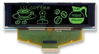
MCOT256064BA-GM
Graphic OLED, 256 x 64, Green on Black, 2.8V, Multi, 88mm x 27.8mm, -30 °C
⚠️ Reference pricing provided. In case of supply shortages, we will connect you with our trusted procurement partners to ensure your project's continuity.
- Manufacturer: MIDAS
- Product type: Graphic OLED Displays
- Resolution: 256 x 64
- Module Size: 88mm x 27.8mm
- Logic Voltage: 2.8V
- Product Range: MCOT256064BA
- Interface Type: Multi
- Display Appearance: Green on Black
- Display Construction: COT
- Operating Temperature Max: 85°C
- Operating Temperature Min: -30°C
| Delivery and price | |
|---|---|
| Units per pack | 1 |
| Price | 32.02 € |
| Current stock | 10+ |
| Lead time | 30 days |
Datasheet

Electra House, 32 Southtown Road Great Yarmouth, Norfolk NR31 0DU, England Telephone +44 (0)1493 602602 Fax +44 (0)1493 665111 Email:sales@midasdisplays.com www.midasdisplays.com |MCOT256064BA-GM|MCOT256064BA-GM|256 x 64|256 x 64|OLED Module| |---|---|---|---|---| |**Specification **||||| |Version: 1|||Date: 27/03/2017|| |**Revision**||||| |1|23/03/2017||First Issue|| |DisplayFeatures|DisplayFeatures| |---|---| |Resolution|256 x 64| |Appearance|Green on Black| |Logic Voltage|2.8V| |Interface|Multi| |Module Size|88.00 x 27.80 x 2.00mm| |OperatingTemperature|-40°C ~ +85°C| |Construction|COT| Box Quantity Weight / Display ----- * - For full design functionality, please use this specification in conjunction with the SSD1322 specification. (Provided Separately) |**Display Accessories**|**Display Accessories**| |---|---| |**Part Number**|**Description**| ||Interface board compatible with any| ||display that requires a direct solder| |MPBV4-Iss2|connection to 0.7, 0.8 , 0.845 or 1 mm.| ||Supports any driver board that can be| ||wired to a 2mm pitch 44-way DIL.| |**Optional Variants**|| |---|---| |**Appearance**|**Voltage**| ## **Functions and Features** - 256 x 64 Graphic - Built ‐ in controller - viewing angle Free - Wide Temperature -40 ℃ ~ +85 ℃ (Operating) - RoHS compliant ## **Mechanical Specification** |**Item**|**Description**|| |---|---|---| |Product No.|MCOT256064BA-GM|| |Inch|3.12”|| |Color|Green|| |Active Area|76.78(W)×19.18(H)|mm| |Panel Size|88.00(W)×27.80(H)×2.00(D)|mm| |Dot Size|0.28(W)×0.28(H)|mm| |Dot Pitch|0.3(W)×0.3(H)|mm| |Display Format|256×64|| |Duty Ratio|1/64 Duty|Duty| |Controller|SSD1322 or Equivalent|| |Operation Temperature|-40~85|°C| |Storage Temperature|-40~90|°C| |Response Time|≤10|us| |Assembly|Connector|| **==> picture [171 x 18] intentionally omitted <==** **----- Start of picture text -----**<br> Mechanical Drawing<br>**----- End of picture text -----**<br> ## **Pin Description** ## **Power Supply** |**Power Supply**|**Power Supply**||| |---|---|---|---| |**Pin Number**|**Symbol**|**Type**|**Function**| |26|VCI|P|**Power Supply for Operation**<br>This is a voltage supply pin. It must be connected to external source &<br>always be equal to or higher than VDD & VDDIO.| |25|VDD||**Power Supply for Core Logic Circuit**<br>This is a voltage supply pin. It can be supplied externally (within the range<br>of 2.4~2.6V) or regulated internally from VCI. A capacitor should be<br>connected between this pin & VSS under all circumstances.| |24|VDDIO||**Power Supply for I/O Pin**<br>This pin is a power supply pin of I/O buffer. It should be connected to<br>VDD or external source. All I/O signal should have VIH reference to<br>VDDIO. When I/O signals pins (BS0~BS1, D0~D7, control signals…) pull<br>high, they should be connected to VDDIO.| |2|VSS||**Ground of Logic Circuit**<br>This is a ground pin. It also acts as a reference for the logic pins. It must<br>be connected to external ground.| |3,29|VCC||**Power Supply for OEL Panel**<br>These are the most positive voltage supply pin of the chip. They must be<br>connected to external source.| |5,28|VLSS||**Ground of Analog Circuit**<br>These are the analog ground pins. They should be connected to VSS<br>externally.| |**Testing Pads**|||| |---|---|---|---| |**Pin Number**|**Symbol**|**Type**|**Function**| ||||**This pin is No Connection. Should be left open individually.**| |21|NC|O|| ## **Interface** |**Interface**|||||| |---|---|---|---|---|---| |**Pin Number**|**Symbol**|**Type**|**Function**||| |16<br>17|BS0<br>BS1|I|**Communicating Protocol Select**<br>These pins are MCU interface selection input. See the following table:||| |||||BS1|BS2| ||||3-wire SPI|1|0| ||||4-wire SPI|0|0| ||||8-bit 68xx Parallel|1|1| ||||8-bit 80xx Parallel|0|1| |20|RES#||**Power Reset for Controller and Driver**<br>This pin is reset signal input. When the pin is low, initialization of the chip<br>is executed.||| |19|CS#||**Chip Select**<br>This pin is the chip select input. The chip is enabled for MCU<br>communication only when CS# is pulled low.||| |18|D/C#||**Data/Command Control**<br>This pin is Data/Command control pin. When the pin is pulled high, the<br>input at D7~D0 is treated as display data. When the pin is pulled low, the<br>input at D7~D0 will be transferred to the command register. For detail<br>relationship to MCU interface signals, please refer to the Timing<br>Characteristics Diagrams.||| |14|E/RD#||**Read/Write Enable or Read**<br>This pin is MCU interface input. When interfacing to a 68XX-series<br>microprocessor, this pin will be used as the Enable (E) signal. Read/write<br>operation is initiated when this pin is pulled high and the CS# is pulled<br>low. When connecting to an 80XX-microprocessor, this pin receives the<br>Read (RD#) signal. Data read operation is initiated when this pin is pulled<br>low and CS# is pulled low. When serial mode is selected, this pin must be<br>connected to VSS.||| |15|R/W#||**Read/Write Select or Write**<br>This pin is MCU interface input. When interfacing to a 68XX-series<br>microprocessor, this pin will be used as Read/Write (R/W#) selection<br>input. Pull this pin to “High” for read mode and pull it to “Low” for write<br>mode. When 80XX interface mode is selected, this pin will be the Write<br>(WR#) input. Data write operation is initiated when this pin is pulled low<br>and the CS# is pulled low. When serial or I2C mode is selected, this pin<br>must be connected to VSS.||| **Host Data Input/output Bus** These pins are 8-bit bi-directional data bus to be connected to the 6~13 D7~D0 I/O microprocessor’s data bus. When serial mode is selected, D1 will be the serial data input SDIN and D0 will be the serial clock input SCLK. Unused pins must be connected to VSS except for D2 in serial mode. ~~TT~~ **Reserve Pin Number Symbol Type Function Reserved Pin** 23 N.C. - The N.C. pin between function pins is reserved for compatible and flexible design. **Reserved Pin (Supporting Pin)** N.C. - 1,30 The supporting pins can reduce the influences from stresses on the (GND) function pins. These pins must be connected to external ground. ~~a~~ ## **Block Diagram** MCU Interface Selection: BS0 and BS1 Pins connected to MCU interface: D7~D0, E/RD#, R/W#, D/C#, CS#, and RES# C1, C3, C5: 0.1 μ F C2, C4: 4.7 μ F C6: 10 μ F C7: 1 μ F C8: 4.7 μ F / 25V Tantalum Capacitor R1: 680k Ω, R1 = (Voltage at IREF – VSS) / IREF R2: 50 Ω, 1/4W D1: ≤1.4V, 0.5W ## **DC Characteristics** |**Item**|**Symbol**|**Condition**|**Min.**|**Type**|**Max.**|**Unit**| |---|---|---|---|---|---|---| |Supply Voltage for Operation|VCI||2.4|2.8|3.5|Volt| |Supply Voltage for Logic|VDD||2.4|2.5|2.6|Volt| |Supply Voltage for I/O Pins|VDDIO||1.65|1.8|VCI|Volt| |Supply Voltage for Display|VCC|Note 3|11.5|12|12.5|Volt| |Operating Current for VCI|ICI||-|1.8|2.25|mA| |Operating Current for VCC|ICC|Note 4|-|26.3|32.9|mA| |||Note 5|-|41.1|51.4|mA| |Sleep Mode Current for VCI|ICI,SLEEP||-|1|5|μA| |Sleep Mode Current for VCC|ICC,SLEEP||-|1|5|μA| Note 3: Brightness (Lbr) and Supply Voltage for Display (VCC) are subject to the change of the panel characteristics and the customer’s request. Note 4: VCI = 2.8V, VCC = 12V, 50% Display Area Turn on. Note 5: VCI = 2.8V, VCC = 12V, 100% Display Area Turn on. ## **Optical Characteristics** |Item|Symbol|Conditions|Min.|Typ|Max.|Unit| |---|---|---|---|---|---|---| |Brightness(Green)|Lbr|-||120|-|cd/㎡| |C.I.E. (Green)|(X)<br>(Y)|C.I.E|0.27<br>0.58|0.31<br>0.62|0.35<br>0.66|| |Dark Room Contrast|CR|-|-|>10000:1|-|| |Viewing anglerange|-|-|-|Free|-|Degree| * Optical measurement taken at VDD = 2.8V, VCC = 12V. ## **Absolute Maximum rating** |**Item**|**Symbol**|**Min.**|**Typ.**|**Max.**|**Unit**|**Notes**| |---|---|---|---|---|---|---| |Supply Voltage for Operation|VCI|-0.3|-|4|Volt|1,2| |Supply Voltage for Logic|VDD|-0.5|-|2.75|Volt|1,2| |Supply Voltage for I/O Pins|VDDIO|-0.5|-|VCI|Volt|1,2| |Supply Voltage for Display|Vcc|-0.5|-|16|Volt|1,2| |Life Time (60 cd/㎡)||---|100,000|---|Hour|| Note 1: All the above voltages are on the basis of “VSS = 0V”. Note 2: When this module is used beyond the above absolute maximum ratings, permanent breakage of the module may occur. Also, for normal operations, it is desirable to use this module under the conditions according to Section. “Optics”. If this module is used beyond these conditions, malfunctioning of the module can occur and the reliability of the module may deteriorate. ## **AC Characteristics** Please refer “SSD1322 specification. ## **Actual Application Example** Command usage and explanation of an actual example <Initialization> If the noise is accidentally occurred at the displaying window during the operation, please reset the display in order to recover the display function.
Updated at February 9, 2023
About Novapart
Novapart is a B2B electronic component broker specialising in stock shortages and cost reduction. We source hard-to-find parts and identify compliant alternatives across a catalogue of 410,000+ components from 500+ manufacturers.
Learn more →Stock Shortage Specialist
When a component is unavailable, discontinued or has an unacceptable lead time, we tap into our network of vetted European and Asian distributors to source what you need — without compromising on quality or traceability.
Request a quote →Compliant Alternatives
We identify pin-to-pin, electrically equivalent substitutes that meet the same certifications (RoHS, AEC-Q100, REACH) as your original specification — validated against datasheets, not just part numbers. Often at a lower cost.
BOM Analysis service →