
Image not available
Illustrative purposes only

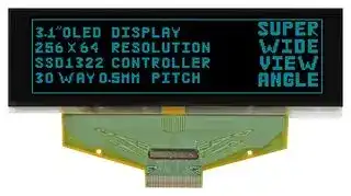
MCOT256064B1A-BM
Graphic OLED, 256 x 64 Pixels, Blue on Black, 2.5V, Multi, 88mm x 27.8mm, -40 °C
⚠️ Reference pricing provided. In case of supply shortages, we will connect you with our trusted procurement partners to ensure your project's continuity.
- Manufacturer: MIDAS
- Product type: Graphic OLED Displays
- Resolution: 256 x 64 Pixels
- Module Size: 88mm x 27.8mm
- Logic Voltage: 2.5V
- Interface Type: Multi
- Display Appearance: Blue on Black
- Display Construction: COT
- Operating Temperature Max: 70°C
- Operating Temperature Min: -40°C
| Delivery and price | |
|---|---|
| Units per pack | 50 |
| Price | 33.47 € |
| Current stock | 10+ |
| Lead time | 30 days |
Datasheet

Electra House, 32 Southtown Road Great Yarmouth, Norfolk NR31 0DU, England

Telephone +44 (0)1493 602602 Fax +44 (0)1493 665111 Email:sales@midasdisplays.com www.midasdisplays.com

|MCOT256064B1A-BM|MCOT256064B1A-BM|256 x 64|256 x 64|OLED Module|
|---|---|---|---|---|
|**Specification**|||||
|Version:    1|||Date:05/09/2019||
|**Revision**|||||
|1|02/09/2019||First Issue||


## Display Features

|Resolution|256 x 64|
|---|---|
|Appearance|Blue on Black|
|Logic Voltage|2.5V|
|Interface|Multi|
|Module Size|88.00 x 27.80 x 2.05mm|
|OperatingTemperature|-40°C ~ +70°C|
|Construction|COT|


Box Quantity Weight / Display -----

* - For full design functionality, please use this specification in conjunction with the SSD1322 specification. (Provided Separately)

|**Display Accessories**|**Display Accessories**|
|---|---|
|**Part Number**|**Description**|
||Interface board compatible with any|
||display that requires a direct solder|
|MPBV4-Iss2|connection to 0.7, 0.8 , 0.845 or 1 mm.|
||Supports any driver board that can be|
||wired to a 2mm pitch 44-way DIL.|


|**Optional Variants**||
|---|---|
|**Appearance**|**Voltage**|


## **General Specification**

The Features is described as follow:

- Module dimension: 88.0 × 27.8 × 2.05 mm

- Active area: 76.778 `×` 19.178 mm

- Dot Matrix : 256 `×` 64

- Dot Size: 0.278 `×` 0.278 mm

- Dot Pitch: 0.3 `×` 0.3mm

- Display Mode: Passive Matrix

- Duty: 1/64

- Display Color: Sky Blue

- IC: SSD1322

- Interface: 6800,8080,SPI

- Size: 3.12 inch

## **Interface Pin Function**

|**Pin**<br>**Number**|**Symbol**|**I/O Function**|**I/O Function**|
|---|---|---|---|
|**_Power Supply_**||||
|**26**|**VCI**|P|**_Power Supply for Operation_**<br>This is a voltage supply pin. It must be connected to<br>external source & always be equal to or higher than VDD<br>& VDDIO.|
|**25**|**VDD**|P|**_Power Supply for Core Logic Circuit_**<br>This is a voltage supply pin. It can be supplied externally (within<br>the range of 2.4~2.6V) or regulated internally from VCI. A<br>capacitor should be connected between this pin & VSS under<br>all circumstances.|
|**24**|**VDDIO**|P|**_Power Supply for I/O Pin_**<br>This pin is a power supply pin of I/O buffer. It should be<br>connected to VDD or external source. All I/O signal should have<br>VIH reference to VDDIO. When I/O signal pins (BS0~BS1,<br>D0~D7, control signals…) pull high, they should be connected<br>to VDDIO.|
|**2**|**VSS**|P|**_Ground of Logic Circuit_**<br>This is a ground pin. It also acts as a reference for the logic<br>pins. It must be connected to external ground.|
|**3,29**|**VCC**|P|**_Power Supply for OLED Panel_**<br>These are the most positive voltage supply pin of the chip. They<br>must be connected to external source.|
|**5,28**|**VLSS**|P|**_Ground of Analog Circuit_**<br>These are the analog ground pins. They should be connected<br>to VSS externally.|
|**_Driver_**||||
|**22**|**IREF**|I|**_Current Reference for Brightness Adjustment_**<br>This pin is segment current reference pin. A resistor should be<br>connected between this pin and VSS. Set the current lower<br>than 10uA.|
|**4**|**VCOMH**|P|**_Voltage Output High Level for COM Signal_**<br>This pin is the input pin for the voltage output high level for<br>COM signals. A tantalum capacitor should be connected<br>between this pin and VSS.|
|**27**|**VSL**|P|**_Voltage Output Low Level for SEG Signal_**<br>This is segment voltage reference pin.<br>When external VSL is not used, this pin should be left open.<br>When external VSL is used, this pin should connect with<br>resistor and diode to ground.|


|~~TT~~|~~TT~~|~~TT~~|~~TT~~|
|---|---|---|---|
|**_Testing Pads_**<br>~~TT~~||||
|**21**<br>~~TT~~|**FR**<br>~~TT~~|O|**_Frame Frequency Triggering Signal_**<br>This pin will send out a signal that could be used to identify the<br>driver status. Nothing should be connected to this pin. It should<br>be left open individually.|
|**16**<br>~~ee~~|**BS0**<br>~~ee~~|I|**_Communicating Protocol Select_**<br>These pins are MCU interface selection input. See the following<br>table:<br>sos]<br>a<br>p4wieSPL<br>|<br>[oT<br>[8-bit 8XXParallel | fa<br>~~[-8:bit6OXXParallel|oT~~|
|**17**<br>~~ee~~|**BS1**<br>~~ee~~|||
|**20**|**RES#**|I|**_Power Reset for Controller and Driver_**<br>This pin is reset signal input. When the pin is low, initialization<br>of the chip is executed.<br>~~[-8:bit 6OXXParallel | oT~~|
|**19**|**CS#**|I|**_Chip Select_**<br>This pin is the chip select input. The chip is enabled for MCU<br>communication only when CS# is pulled low.|
|**18**|**D/C#**|I|**_Data/Command Control_**<br>This pin is Data/Command control pin. When the pin is pulled<br>high, the input at D7~D0 is treated as display data.<br>When the pin is pulled low, the input at D7~D0 will be<br>transferred to the command register. For detail relationship to<br>MCU interface signals, please refer to the<br>Timing Characteristics Diagrams.|
|**14**|**E/RD#**|I|**_Read/Write Enable or Read_**<br>This pin is MCU interface input. When interfacing to a<br>68XX-series microprocessor, this pin will be used as the<br>Enable (E) signal. Read/write operation is initiated when this<br>pin is pulled high and the CS# is pulled low.<br>When connecting to an 80XX-microprocessor, this pin receives<br>the Read (RD#) signal. Data read operation is initiated when<br>this pin is pulled low and CS# is pulled low.<br>When serial mode is selected, this pin must be connected to<br>VSS.|
|**15**|**R/W#**|I|**_Read/Write Select or Write_**<br>This pin is MCU interface input. When interfacing to a<br>68XX-series microprocessor, this pin will be used as<br>Read/Write (R/W#) selection input. Pull this pin to “High” for<br>read mode and pull it to “Low” for write mode.<br>When 80XX interface mode is selected, this pin will be the<br>Write (WR#) input. Data write operation is initiated when this<br>pin is pulled low and the CS# is pulled low.<br>When serial mode is selected, this pin must be connected to<br>VSS.|
|**6~13**|**D7~D0**|I/O|**_Host Data Input/Output Bus_**<br>These pins are 8-bit bi-directional data bus to be connected to<br>the microprocessor’s data bus. When serial mode is selected,|


||||D1 will be the serial data input SDIN and D0 will be the serial<br>clock input SCLK.<br>Unused pins must be connected to VSS except for D2 in serial<br>mode.|
|---|---|---|---|
|**_Reserve_**||||
|**23**|**N.C.**|-|**_Reserved Pin_**<br>The N.C. pin between function pins are reserved for compatible<br>and flexible design.|
|**1,30**|**N.C.**<br>**(GND)**|-|**_Reserved Pin_**(Supporting Pin)<br>The supporting pins can reduce the influences from stresses<br>on the function pins. These pins must be connected to external<br>ground.|


## **Contour Drawing & Block Diagram**

**==> picture [455 x 671] intentionally omitted <==**

**----- Start of picture text -----**<br>
27.8¡ 0Ó.3(Panel Size)<br>! ! 25.8(Cap Size)<br>7 — _<br>19.7¡ Ó0.3<br>24.8¡ Ó0.3(Polarizer) 0.5¡ Ó0.5<br>11.01<br>21.18(VA) 2.0<br>9.2<br>19.178(AA) 3.0<br>8.7<br>4.36<br>4.0<br>3.0<br>i | ee ee |<br>!<br>A<br>A<br>!<br>Aoaey<br>A<br>1! |<br>' j<br>! |<br>Y oroy<br>wr<br>oy yy, aN on<br>| ~ |<br>0.3<br>4.0<br>0.278<br>io<br>r oy<br>(Row 1) Common A63 (Row 64) Common A0<br>(Column 1) Segment 112 (Column 128) Segment 239<br>(Column 256) Segment 357 5.61 4.61 0.5¡ Ó0.5<br>(Column 129) Segment 240<br>        (Row 1) Common B63 (Row 64) Common B0<br>14.0<br>0.5<br>1<br>60.0¡ Ó0.2 40.0¡ Ó0.1 15.50 P0.5*29=14.5 0.3 SSD1322 256*64 Pixels Active Area 3.12"  76.778(AA) 78.78(VA) 87.0¡ Ó0.3(Polarizer) 88.0¡ Ó0.3(Cap Size) 88.0¡ 0Ó.3(Panel Size)<br>30<br>2-R0.5¡ Ó0.05<br>T=0.15Max REMOVE TAPE<br>Contact Side<br>0.8MAX 0.3¡ Ó0.05 Polarizer<br>Stiffener 1.1 0.7 2.05<br>0.3<br>The non-specified tolerance of dimension is<br>SCALE 30/1 DOT SIZE<br>0.278<br>30 29 28 27 26 25 24 23 22 21 20 19 18 17 16 15 14 13 12 11 10 9 8 7 6 5 4 3 2 1<br>0.3mm.<br>NC(GND) VCC VLSS VSL VCI VDD VDDIO NC IREF FR RES# CS# DC# BS1 BS0 R/W# E/RD# D0 D1 D2 D3 D4 D5 D6 D7 VLSS VCOMH VCC VSS NC(GND)<br>**----- End of picture text -----**<br>


## **FUNCTION BLOCK DIAGRAM**

*For more information, please refer to Application Note provided by Midas Displays.

## **Absolute Maximum Ratings**

|**Parameter**|**Symbol**|**Min**|**Max**|**Unit**<br>**Notes**|**Notes**|
|---|---|---|---|---|---|
|Supply Voltage for<br>Operation|VCI|-0.3|4|V<br>1, 2|1, 2|
|Supply Voltage for Logic|VDD|-0.5|2.75|V<br>1, 2|1, 2|
|Supply Voltage for I/O Pins VDDIO|Supply Voltage for I/O Pins VDDIO|-0.5|VCI|V<br>1, 2|1, 2|
|Supply Voltage for Display|VCC|-0.5|20|V<br>1, 2|1, 2|
|Operating Temperature|TOP|-40|70|°C<br>-|-|
|Storage Temperature|TSTG|-40|85|°C<br>-|-|


Note 1: All the above voltages are on the basis of “VSS = 0V”. Note 2: When this module is used beyond the above absolute maximum ratings, permanent breakage of the module may occur. Also, for normal operations, it is desirable to use this module under the conditions according to Section 6 ‘’Electrical Characteristics’’. If this module is used beyond these conditions, malfunctioning of the module can occur and the reliability of the module may deteriorate

## **Electrical Characteristics**

|**Item**|**Symbol**|**Condition**|**Min**|**Typ**|**Max**|**Unit**|
|---|---|---|---|---|---|---|
|Supply Voltage for Logic|VDD|-|2.4|2.5|2.6|V|
|Power Supply for I/O pins VDDIO|Power Supply for I/O pins VDDIO|-|1.65|3.0|VCI|V|
|Low voltage power supply|VCI|-|2.4|3.0|3.5|V|
|Supply Voltage for Display|Supply Voltage for Display<br>VCC|-|14.0|14.5|15.0|V|
|High Level Input|VIH|-|0.8×VDDIO|-|VDDIO|V|
|Low Level Input|VIL|-|0|-|0.2×VDDIO|V|
|High Level Output|VOH|-|0.9×VDDIO|-|VDDIO|V|
|Low Level Output|VOL|-|0|-|0.1×VDDIO|V|
|50% Check Board operating<br>Current||VCC =14.5V|25.0|26.0|32.0|mA|


## **Optical Characteristics**

|**Item**|**Symbol**|**Condition**|**Min**|**Typ**|**Max**|**Unit**|
|---|---|---|---|---|---|---|
|View Angle|(V)θ|-|160|-|-|deg|
||(H)φ|-|160|-|-|deg|
|Contrast Ratio|CR|Dark|2000:1|-|-|-|
|Response Time|T rise|-|-|10|-|μs|
||T fall|-|-|10|-|μs|
|Display with 50% check Board Brightness|||60|80|-|cd/m2|
|CIEx(Skyblue)||(CIE1931)|0.12|0.16|0.20|-|
|CIEy(Skyblue)||(CIE1931)|0.22|0.26|0.30|-|


## **OLED Lifetime**

|**ITEM**|**Conditions**|**Min**|**Typ**|**Remark**|
|---|---|---|---|---|
|Operating<br>Life Time|Ta=25°C<br>/ Initial 50% check board<br>brightness Typical Value|20,000 Hrs|-|Note|


## Notes:

1. Life time is defined the amount of time when the luminance has decayed to <50% of the initial value.

2. This analysis method uses life data obtained under accelerated conditions to extrapolate an estimated probability density function ( _pdf_ ) for the product under normal use conditions.

3. Screen saving mode will extend OLED lifetime.

## **Reliability**

## **Content of Reliability Test**

|**Content of Reliability Testy Test Test**|**Content of Reliability Testy Test Test**|**Content of Reliability Testy Test Test**|**Content of Reliability Testy Test Test**|**Content of Reliability Testy Test Test**|
|---|---|---|---|---|
|**Environmental Test**|||||
|**Test Item**|**Content of Test**|**Test Condition**|**Applicable**<br>**Standard**||
|High<br>Temperature<br>storage|Endurance test applying the high<br>storage temperature for a long time.|85℃<br>240hrs|——||
|Low<br>Temperature<br>storage|Endurance test applying the low storage<br>temperature for a long time.|Endurance test applying the low storage<br>-40℃<br>240hrs|——||
|High<br>Temperature<br>Operation|Endurance test applying the electric<br>stress (Voltage & Current) and the<br>thermal stress to the element for a long<br>time.|70℃<br>240hrs|——||
|Low<br>Temperature<br>Operation|Endurance test applying the electric<br>stress under low temperature for a long<br>time.|-40℃<br>240hrs|——||
|High<br>Temperature/<br>Humidity<br>Storage|Endurance test applying the high<br>temperature and high humidity storage<br>for a long time.|60℃,90%RH<br>240hrs|——||
|High<br>Temperature/<br>Humidity<br>Operation|Endurance test applying the high<br>temperature and high humidity<br>Operation for a long time.|60℃,90%RH<br>120hrs|||
|Temperature<br>Cycle|Endurance test applying the low and<br>high temperature cycle.<br>-40℃25℃80℃<br>30min    5min     30min<br>1cycle|-40℃/80℃<br>30 cycles|——||
|Mechanical Test|||||
|Vibration test|Endurance test applying the vibration<br>during transportation and using.|Frequency:10~55Hz<br>amplitude:1.5mm<br>Time:0.5hrs/axis<br>Test axis:X,Y,Z|——||
|Others|||||
|Static<br>electricity test|Endurance test applying the electric<br>stress to the finished product housing.|Air Discharge model<br>±4kv,10 times||——|


*** Supply voltage for OLED system =Operating voltage at 25 ℃

## **Test and measurement conditions**

1. All measurements shall not be started until the specimens attain to temperature stability. After the completion of the described reliability test, the samples were left at room temperature for 2 hrs prior to conducting the failure test at 23±5°C; 55±15% RH.

2. All-pixels-on is used as operation test pattern.

3. The degradation of Polarizer are ignored for High Temperature storage, High Temperature/ Humidity Storage, Temperature Cycle

## **Evaluation criteria**

1. The function test is OK.

2. No observable defects.

3. Luminance: > 50% of initial value.

4. Current consumption: within ± 50% of initial value.

## **APPENDIX:**

## **RESIDUE IMAGE**

Because the pixels are lighted in different time, the luminance of active pixels may reduce or differ from inactive pixels. Therefore, the residue image will occur. To avoid the residue image, every pixel needs to be lighted up uniformly.

**Inspection specification**

NO Item Criterion AQL 01 Electrical 1.1 Missing vertical, horizontal segment, segment contrast Testing defect. 1.2 Missing character , dot or icon. 1.3 Display malfunction. 1.4 No function or no display. 0.65 1.5 Current consumption exceeds product specifications. 1.6 OLED viewing angle defect. 1.7 Mixed product types. 1.8 Contrast defect. ~~al~~ 02 Black or 2.1 White and black spots on display ≦ 0.25mm, no more than white three white or black spots present. spots on 2.2 Densely spaced: No more than two spots or lines within 2.5 OLED 3mm. (display only) 03 OLED 3.1 Round type : As black following drawing SIZE Acceptable Q ~~a~~ spots, Φ=( x + y ) / 2 ~~l~~ TY white Φ ≦ 0.10 Accept no spots, dense contamina 0.10 < 2 tion Φ ≦ 0.20 (non-displ 0.20 < 1 ay) Φ ≦ 0.25 0.25 < Φ 0 |IN ~~AS~~ 3.2 Line type : (As following drawing) Length Width Acceptable Q TY --W ≦ 0.02 Accept no dense 2.5 L ≦ 3.0 0.02 < W ≦ 0.03 2 L ≦ 2.5 0.03 < W ≦ 0.05 --0.05 < W As round type ~~===~~ 04 Polarizer bubbles If bubbles are visible, Size Φ Acceptable Q TY judge using black spot Φ ≦ 0.20 Accept no dense specifications, not easy 0.20 < Φ ≦ 0.50 3 2.5 to find, must check in 0.50 < Φ ≦ 1.00 2 specify direction. 1.00 < Φ 0 Total Q TY 3 ~~TT ==~~

|NO<br>~~a~~|Item<br>~~a~~|Criterion<br>~~a~~|AQL<br>~~a~~|
|---|---|---|---|
|05<br>~~a~~<br>~~a~~|Scratches<br>~~a~~<br>~~a~~|Follow NO.3 OLED black spots, white spots, contamination<br>~~a~~<br>~~a~~|~~a~~<br>~~a~~|
|06<br>~~a~~|Chipped<br>glass<br>~~a~~|Symbols Define:<br>x: Chip length      y: Chip width     z: Chip thickness<br>k: Seal width       t: Glass thickness  a: OLED side length<br>L: Electrode pad length:<br>6.1 General glass chip :<br>6.1.1 Chip on panel surface and crack between panels:<br>z: Chip thickness<br>y: Chip width<br>x: Chip length<br>Z≦1/2t<br>Not over viewing<br>area<br>x≦1/8a<br>1/2t<z≦2t<br>Not exceed 1/3k<br>x≦1/8a<br>☉If there are 2 or more chips, x is total length of each chip.<br>6.1.2 Corner crack:<br>z: Chip thickness<br>y: Chip width<br>x: Chip length<br>Z≦1/2t<br>Not over viewing<br>area<br>x≦1/8a<br>1/2t<z≦2t<br>Not exceed 1/3k<br>x≦1/8a<br>☉If there are 2 or more chips, x is the total length of each chip.<br>~~a~~<br>Ve|2.5<br>~~a~~|


**==> picture [475 x 508] intentionally omitted <==**

**----- Start of picture text -----**<br>
a NO Item  Criterion  AQL<br>Symbols :<br>x: Chip length      y: Chip width     z: Chip thickness<br>k: Seal width       t: Glass thickness  a: OLED side length<br>L: Electrode pad length<br>6.2 Protrusion over terminal :<br>6.2.1 Chip on electrode pad :<br>Z<br>y: Chip width  x: Chip length  z: Chip thickness<br>y ≦ 0.5mm  x ≦ 1/8a  0  <  z  ≦  t<br>6.2.2 Non-conductive portion:<br>L L,<br>Glass<br>06  2.5<br>crack<br>K A<br>y: Chip width  x: Chip length  z: Chip<br>thickness<br>y ≦  L  x ≦ 1/8a  0  <  z  ≦  t<br>☉ If the chipped area touches the ITO terminal, over 2/3 of the ITO<br>must remain and be inspected according to electrode terminal<br>specifications.<br>☉ If the product will be heat sealed by the customer, the alignment<br>mark not be damaged.<br>6.2.3 Substrate protuberance and internal crack.<br>x<br>y: width  x: length<br>y ≦ 1/3L  x  ≦  a<br>**----- End of picture text -----**<br>


|NO|Item|Criterion|AQL|
|---|---|---|---|
|07|Cracked<br>glass|The OLED with extensive crack is not acceptable.|2.5|
|08|Backlight<br>elements|8.1 Illumination source flickers when lit.<br>8.2 Spots or scratched that appear when lit must be judged.<br>Using OLED spot, lines and contamination standards.<br>8.3 Backlight doesn’t light or color wrong.|0.65<br>2.5<br>0.65|
|09|Bezel|9.1 Bezel may not have rust, be deformed or have<br>fingerprints, stains or other contamination.<br>9.2 Bezel must comply with job specifications.|2.5<br>0.65|
|10|PCB、COB|10.1 COB seal may not have pinholes larger than 0.2mm or<br>contamination.<br>10.2 COB seal surface may not have pinholes through to the<br>IC.<br>10.3 The height of the COB should not exceed the height<br>indicated in the assembly diagram.<br>10.4 There may not be more than 2mm of sealant outside the<br>seal area on the PCB. And there should be no more than<br>three places.<br>10.5 No oxidation or contamination PCB terminals.<br>10.6 Parts on PCB must be the same as on the production<br>characteristic chart. There should be no wrong parts,<br>missing parts or excess parts.<br>10.7 The jumper on the PCB should conform to the product<br>characteristic chart.<br>10.8 If solder gets on bezel tab pads, OLED pad, zebra pad<br>or screw hold pad, make sure it is smoothed down.|2.5<br>2.5<br>0.65<br>2.5<br>2.5<br>0.65<br>0.65<br>2.5|
|11|Soldering|11.1 No un-melted solder paste may be present on the PCB.<br>11.2 No cold solder joints, missing solder connections,<br>oxidation or icicle.<br>11.3 No residue or solder balls on PCB.<br>11.4 No short circuits in components on PCB.|2.5<br>2.5<br>2.5<br>0.65|


|NO|Item|Criterion|AQL|
|---|---|---|---|
|12|General<br>appearance|12.1 No oxidation, contamination, curves or, bends on<br>interface Pin (OLB) of TCP.<br>12.2 No cracks on interface pin (OLB) of TCP.<br>12.3 No contamination, solder residue or solder balls on<br>product.<br>12.4 The IC on the TCP may not be damaged, circuits.<br>12.5 The uppermost edge of the protective strip on the<br>interface pin must be present or look as if it cause the<br>interface pin to sever.<br>12.6 The residual rosin or tin oil of soldering (component or<br>chip component) is not burned into brown or black color.<br>12.7 Sealant on top of the ITO circuit has not hardened.<br>12.8 Pin type must match type in specification sheet.<br>12.9 OLED pin loose or missing pins.<br>12.10 Product packaging must the same as specified on<br>packaging specification sheet.<br>12.11 Product dimension and structure must conform to<br>product specification sheet.|2.5<br>0.65<br>2.5<br>2.5<br>2.5<br>2.5<br>2.5<br>0.65<br>0.65<br>0.65<br>0.65|


**Check Item Classification Criteria** No Display Major Missing Line Major ~~a~~ Pixel Short Major ~~| wi |~~ Darker Short Major ~~ee, |~~ Wrong Display Major ~~on |~~ Un-uniform B/A x 100% < 70% Major A/C x 100% < 70% ~~oF~~

## **Precautions in use of OLED Modules**

- (1) Avoid applying excessive shocks to module or making any alterations or modifications to it.

- (2) Don’t make extra holes on the printed circuit board, change the components or modify its shape of OLED display module.

- (3) Don’t disassemble the OLED display module.

- (4) Do not apply input signals while the logic power is off.

- (5) Don’t operate it above the absolute maximum rating.

- (6) Don’t drop, bend or twist OLED display module.

- (7) Soldering: only to the I/O terminals.

- (8) Hot-Bar FPC soldering condition: 280~350C, less than 5 seconds.

- (9) Midas has the right to change the passive components (Resistors, capacitors and other passive components will have different appearance and color caused by the different supplier.) and change the PCB Rev. (In order to satisfy the supplying stability, management optimization and the best product performance...etc, under the premise of not affecting the electrical characteristics and external dimensions, Midas have the right to modify the version.)

- (10) Midas has the right to upgrade or modify the product function.

## **1. Handling Precautions**

- (1) Since the display panel is being made of glass, do not apply mechanical impacts such as dropping from a high position.

- (2) If the display panel is broken by some accident and the internal organic substance leaks out, be careful not to inhale nor lick the organic substance.

- (3) If pressure is applied to the display surface or its neighborhood of the OLED display module, the cell structure may be damaged. So, be careful not to apply pressure to these sections.

- (4) The polarizer covering the surface of the OLED display module is soft and easily scratched.

- (5) When the surface of the polarizer of the OLED display module has soil, clean the surface. It takes advantage by using following adhesion tape.

   - Scotch Mending Tape No. 810 or an equivalent

   - Never try to breathe upon the soiled surface nor wipe the surface using cloth containing solvent such as ethyl alcohol, since the surface of the polarizer will become cloudy. Also, pay attention that the following liquid and solvent may spoil the polarizer:

   - Water

   - Ketone

   - Aromatic Solvents

- (6) Protection film is being applied to the surface of the display panel and removes the protection film before assembling it. At this time, if the OLED display module has been stored for a long period of time, residue adhesive material of the protection film may remain on the surface of the display panel after removed of the film. In such case, remove the residue material by the method introduced in the above Section 5.

- (7) Do not touch the following sections whenever possible while handling the OLED display modules.

   - Pins and electrodes

   - Pattern layouts such as the TCP & FPC

- (8) Hold OLED display module very carefully when placing OLED display module into the System housing. Do not apply excessive stress or pressure to OLED display module. And, do not over bend the film with electrode pattern layouts. These stresses will influence the display performance. Also, secure sufficient rigidity for the outer cases.

- (9) Do not apply stress to the LSI chips and the surrounding molded sections.

- (10) Pay sufficient attention to the working environments when handing OLED display modules to prevent occurrence of element breakage accidents by static electricity.

   - Be sure to make human body grounding when handling OLED display modules.

   - Be sure to ground tools to use or assembly such as soldering irons.

   - To suppress generation of static electricity, avoid carrying out assembly work under dry

   - environments.

* Protective film is being applied to the surface of the display panel of the OLED display module. Be careful since static electricity may be generated when exfoliating the protective film.

## **2. Storage Precautions**

- (1) When storing OLED display modules, put them in static electricity preventive bags to avoid be directly exposed to sun or lights of fluorescent lamps. (We recommend you to store these modules in the packaged state when they were shipped from Midas. At that time, be careful not to let water drops adhere to the packages or bags.)

- (2) When the OLED display module is being dewed or when it is placed under high temperature or high humidity environments, the electrodes may be corroded if electric current is applied. Please store it in clean environment.

## **3. Designing Precautions**

- (1) The absolute maximum ratings are the ratings which cannot be exceeded for OLED display module, and if these values are exceeded, OLED display module may be damaged.

- (2) To prevent occurrence of malfunctioning by noise, pay attention to satisfy the VIL and VIH specification and to make the signal line cable as short as possible.

- (3) We recommend you to install excess current preventive unit (fuses, etc.) to the power circuit (VDD / VCC). (Recommend value: 0.5A)

- (4) Pay sufficient attention to avoid occurrence of mutual noise interference with the nearby devices.

- (5) As for EMI, take necessary measures on the equipment side basically.

- (6) If the power supplied to the OLED display module is forcibly shut down by such errors as taking out the main battery while the OLED display panel is in operation, we cannot guarantee the quality of this OLED display module.

   - Connection (contact) to any other potential than the above may lead to rupture of the IC.

- (7) If this OLED driver is exposed to light, malfunctioning may occur and semiconductor elements may change their characteristics.

- (8) The internal status may be changed, if excessive external noise enters into the module. Therefore, it is necessary to take appropriate measures to suppress noise generation or to protect module from influences of noise on the system design.

- (9) We recommend you to make periodical refreshment of the operation statuses (re-setting of

the commands and re-transference of the display data) to cope with catastrophic noise.

- (10) It's pretty common to use "Screen Saver" to extend the lifetime and Don't use the same image for long time in real application. When an OLED display module is operated for a long of time with fixed pattern, an afterimage or slight contrast deviation may occur.

- (11) The limitation of FPC and Film bending.

(12) The module should be fixed balanced into the housing, or the module may be twisted.

**==> picture [254 x 50] intentionally omitted <==**

**----- Start of picture text -----**<br>
0.1<br>aan<br>(0.1 Max.)<br>**----- End of picture text -----**<br>


## **4. Precautions when disposing of the OLED display modules**

- (1) Request the qualified companies to handle industrial wastes when disposing of the OLED display modules. Or, when burning them, be sure to observe the environmental and hygienic laws and regulations.
Updated at February 9, 2023
About Novapart
Novapart is a B2B electronic component broker specialising in stock shortages and cost reduction. We source hard-to-find parts and identify compliant alternatives across a catalogue of 410,000+ components from 500+ manufacturers.
Learn more →Stock Shortage Specialist
When a component is unavailable, discontinued or has an unacceptable lead time, we tap into our network of vetted European and Asian distributors to source what you need — without compromising on quality or traceability.
Request a quote →Compliant Alternatives
We identify pin-to-pin, electrically equivalent substitutes that meet the same certifications (RoHS, AEC-Q100, REACH) as your original specification — validated against datasheets, not just part numbers. Often at a lower cost.
BOM Analysis service →