
Image not available
Illustrative purposes only

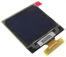
MCOT128128BV-WM
Graphic OLED, 128 x 128, White on Black, 2.8V, I2C, Parallel, SPI, 33.8mm x 43.7mm, -40 °C
⚠️ Reference pricing provided. In case of supply shortages, we will connect you with our trusted procurement partners to ensure your project's continuity.
- Manufacturer: MIDAS
- Product type: Graphic OLED Displays
- Resolution: 128 x 128
- Module Size: 33.8mm x 43.7mm
- Logic Voltage: 2.8V
- Product Range: MCOT128128BV
- Interface Type: I2C, Parallel, SPI
- Display Appearance: White on Black
- Display Construction: TAB
- Operating Temperature Max: 70°C
- Operating Temperature Min: -40°C
| Delivery and price | |
|---|---|
| Units per pack | 50 |
| Price | 12.98 € |
| Current stock | 10+ |
| Lead time | 30 days |
Datasheet

**Midas Components Limited Telephone** +44 (0)1493 602602 Electra House **Fax** +44 (0)1493 665111 32 Southtown Road **Email** sales@midasdisplays.com Great Yarmouth **Website** www.midasdisplays.com Norfolk NR31 0DU England

**S ecification p** Part Number: ~~|~~ Version: ~~meoranaaee ee~~ Date: ~~a~~ **Revision** ~~|~~ **No.** ~~N~~ **Date** ~~git~~ **Description** ~~Vs)~~ **Item** ~~er,~~ **Page**

## **REVISION RECORD**

REV. REVISION DESCRIPTION REV. DATE REMARK

## **CONTENTS**

|**CONTENTS**||
|---|---|
|ITEM|PAGE|
|**1. SCOPE**|4|
|**2. WARRANTY**|4|
|**3. FEATURES**|4|
|**4. MECHANICAL DATA**|5|
|**5. MAXIMUM RATINGS**|6|
|**6. ELECTRICAL CHARACTERISTICS**|7|
|**6.1 D.C ELECTRICALCHARACTERISTICS**||
|**6.2 ELECTRO-OPTICAL CHARACTERISTICS**||
|**7. INTERFACE**|9|
|**7.1 FUNCTION BLOCK DIAGRAM**||
|**7.2 PANEL LAYOUT DIAGRAM**||
|**7.3 PIN ASSIGNMENTS**||
|**7.4 GRAPHIC DISPLAY DATA RAM ADDRESS MAP**||
|**7.5 INTERFACE TIMING CHART**||
|**8. POWER ON / OFF SEQUENCE & APPLICATION CIRCUIT**|15|
|**8.1 POWERON / OFFSEQUENCE **||
|**8.2 APPLICATION CIRCUIT**||
|**8.3 COMMAND TABLE**||
|**9. RELIABILITY TEST CONDITIONS**|17|
|**10. EXTERNAL DIMENSION**|18|
|**10.1 MODULE ASSEMBLY DRAWING**||
|**10.2 FOOTPRINT DRAWING**||


## **1. SCOPE**

The purpose of this specification is to define the general provisions and quality requirements that apply to the supply of display cells manufactured by Midas. This document, together with the Module Assembly Drawing, is the highest-level specification for this product. It describes the product, identifies supporting documents and contains specifications.

## **2. WARRANTY**

Midas warrants that the products delivered pursuant to this specification (or order) will conform to the agreed specifications for twelve (12) months from the shipping date ("Warranty Period"). Midas is obligated to repair or replace the products which are found to be defective or inconsistent with the

specifications during the Warranty Period without charge, on condition that the products are stored or used as the conditions specified in the specifications. Nevertheless, Midas  is not obligated to repair or replace the products without charge if the defects or inconsistency are caused by the force majeure or the reckless behaviors of the customer.

After the Warranty Period, all repairs or replacements of the products are subject to charge.

## **3. FEATURES**

- Small molecular organic light emitting diode.

- Color : White

- Panel resolution : 128*128

- Driver IC : SSD1327

- Excellent Quick response time : 10µs

- Extremely thin thickness for best mechanism design : 1.41 mm

- High contrast : 10000:1

- Wide viewing angle : Free

- Strong environmental resistance.

- 8-bit 6800-series Parallel Interface, 8-bit 8080-series Parallel Interface, Serial Peripheral Interface, I2C Interface.

- Wide range of operating temperature : -40 to 80°C

- Anti-glare polarizer.

## **4. MECHANICAL DATA**

|NO|ITEM|SPECIFICATION|UNIT|
|---|---|---|---|
|1|Dot Matrix|128 x 128|dot|
|2|Dot Size|0.19(W)x 0.19(H)|2<br>mm|
|3|Dot Pitch|0.21(W)x 0.21(H)|2<br>mm|
|4|Aperture Rate|82|%|
|5|Active Area|26.86(W)x 26.86(H)|2<br>mm|
|6|Panel Size|33.8(W)x 36.5(H)|2<br>mm|
|7*|Panel Thickness|1.22±0.1|mm|
|8|Module Size|33.8(W)x 43.7(H)x 1.41(T)|3<br>mm|
|9|Diagonal A/A size|1.5|inch|
|10|Module Weight|3.48±10%|gram|


* Panel thickness includes substrate glass, cover glass and UV glue thickness.

## **5. MAXIMUM RATINGS**

|ITEM|MIN|MAX|UNIT|Condition|Remark|
|---|---|---|---|---|---|
|Supply Voltage (VCI)|-0.3|4|V|Ta = 25°C|IC maximum<br>rating|
|Supply Voltage (Vcc)|8|19|V|Ta = 25°C|IC maximum<br>rating|
|OperatingTemp.|-40|70|°C|||
|Storage Temp|-40|85|°C|||
|Humidity||85|%|||
|Life Time (20K)(typ)|||Hrs|100 cd/m², 50%<br>checkerboard|Note (1)|
|Life Time (25K)(typ)|||Hrs|90 cd/m², 50%<br>checkerboard|Note (2)|
|Life Time (30K)(typ)|||Hrs|80 cd/m², 50%<br>checkerboard|Note (3)|


## Note:

   - (A) Under Vcc = 15V, Ta = 25°C, 50% RH.

   - (B) Life time is defined the amount of time when the luminance has decayed to less than 50% of the initial measured luminance.

- (1) Setting of 100 cd/m2 :

   - Contrast setting : 0x9b

   - Frame rate : 105Hz

   - Duty setting : 1/128

- (2) Setting of 90 cd/m2 :

   - Contrast setting : 0x77

   - Frame rate : 105Hz

   - Duty setting : 1/128

- (3) Setting of 80 cd/m2 :

   - Contrast setting : 0x60

   - Frame rate : 105Hz

   - Duty setting : 1/128

## **6. ELECTRICAL CHARACTERISTICS**

## **6.1 D.C ELECTRICAL CHARACTERISTICS**

|SYMBOL|SYMBOL<br>PARAMETERS|TEST<br>CONDITION|MIN|TYP|MAX|UNIT|
|---|---|---|---|---|---|---|
|VCC|Driver power supply<br>(for OLED panel)|-|14.5|15|15.5|V|
|VCI|Low voltage power<br>supply|-|2.6|-|3.5|V|
|VOH|High logic output level|Iout=100 uA,|0.9*VCI|-|VCI|V|
|VOL|Low logic output level|Iout=100uA,|0|-|0.1*VCI|V|
|VIH|High logic input level|Iout=100uA,|0.8*VCI|-|VCI|V|
|VIL|Low logic input level|Iout=100uA,|0|-|0.2*VCI|V|
|ICC|VCCSupply Current|VCI= 3.5V,<br>VCC= 18V,<br>Display ON,<br>No panel<br>attached,<br>contrast=FF|External<br>VDD= 2.5V|600|750|uA|
||||Internal<br>VDD= 2.5V|600|750||
|ICI|VCISupply Current|VCI= 3.5V,<br>VCC= 18V,<br>Display ON,<br>No panel<br>attached,<br>contrast=FF|External<br>VDD= 2.5V|35|50|uA|
||||Internal<br>VDD= 2.5V|95|120||
|ISEG|Segment output<br>current Setting<br>VCC=18V, IREF=10uA|Contrast=FF|-|300|370|uA|
|||Contrast=AF|-|206|-|uA|
|||Contrast=7F|-|150|-|uA|
|||Contrast=3F|-|75|-|uA|
|||Contrast=1F|-|37.5|-|uA|


## **6.2 ELECTRO-OPTICAL CHARACTERISTICS**

## **PANEL ELECTRICAL SPECIFICATIONS**

|PARAMETER|MIN|TYP.|MAX|UNITS|COMMENTS|
|---|---|---|---|---|---|
|Normal mode current<br>consumption|-|32|34|mA|All pixels on|
|Standby mode<br>current consumption|-|3|4|mA|Standby mode<br>10% pixels on|
|Normal mode power<br>consumption|-|480|510|mW|All pixels on|
|Standby mode power<br>consumption|-|45|60|mW|Standby mode<br>10% pixels on|
|Pixel Luminance|70|90||2<br>cd/m|DisplayAverage|
|StandbyLuminance||20||2<br>cd/m||
|CIEx(White)|0.24|0.28|0.32||CIE1931|
|CIEy (White)|0.28|0.32|0.36||CIE1931|
|Dark Room Contrast|10000:1|10000:1||||
|ViewingAngle|fF|fF<br>Free||degree||
|Response Time||10||µs||


- Driving Voltage : 15V

- Contrast setting : 0x77

- Frame rate : 105Hz

- Duty setting : 1/128 Standby mode condition :

- Driving Voltage : 15V

- Contrast setting : 0x14

- Frame rate : 105Hz

- Duty setting : 1/128

## **7. INTERFACE**

## **7.1 FUNCTION BLOCK DIAGRAM**

## **7.2 PANEL LAYOUT DIAGRAM**

## **7.3 PIN ASSIGNMENTS**

|PIN<br>NAME|PIN NO|DESCRIPTION|
|---|---|---|
|VSS|1|Ground.|
|VCC|2|Power supply for analog circuit.|
|VCOMH|3|Com Voltage Output. A capacitor should be connected<br>between this pin and VSS.|
|GPIO|4|General I/O port.|
|VCI|5|Power supply for logic circuit.|
|VDD|6|A capacitor should be connected between this pin and<br>VSS.|
|BS1|7|MCU bus interface selection pins.|
|BS2|8|MCU bus interface selection pins.|
|VSS|9|Ground.|
|IREF|10|Reference current input pin.<br>A resistor should be connected between this pin and VSS.|
|CS#|11|Chip select input.|
|RES#|12|Reset signal input.<br>When it’s low, initialization of SSD1327 is executed.|
|D/C|13|Data/ Command control.<br>Pull high for write/read display data.<br>Pull low for write command or read status.|
|WR#|14|MCU interface input.<br>Data write operation is initiated when it’s pull low.|
|RD#|15|MCU interface input.<br>Data read operation is initiated when it’s pull low.|
|D0|16|Data bus(for parallel interface)|
|D1|17||
|D2|18||
|D3|19||
|D4|20||
|D5|21||
|D6|22||
|D7|23||
|VCC|24|Power supply for analog circuit.|
|VSS|25|Ground.|


## **7.4 GRAPHIC DISPLAY DATA RAM ADDRESS MAP**

The GDDRAM is a bit mapped static RAM holding the bit pattern to be displayed. The size of the RAM is 128x128x4 bits. For mechanical flexibility, re-mapping on both Segment and Common outputs can be selected by software. The GDDRAM address maps below tables show some examples on using the command “Set Re-map” A0h to re-map the GDDRAM. In the following tables, the lower nibble and higher nibble of D0, D1, D2 … D8189, D8190, D8191 represent the 128x128 data bytes in the GDDRAM.

The GDDRAM map under the following condition: Command “Set Re-map” A0h is set to: Disable Column Address Re-map (A[0]=0) Disable Nibble Re-map (A[1]=0) Enable Horizontal Address Increment (A[2]=0) Disable COM Re-map (A[4]=0) Display Start Line=00h Data byte sequence: D0, D1, D2 … D8191

The GDDRAM map under the following condition: Command “Set Re-map” A0h is set to:

Disable Column Address Re-map (A[0]=0) Disable Nibble Re-map (A[1]=0) Enable Vertical Address Increment (A[2]=1) Disable COM Re-map (A[4]=0) Display Start Line=00h Data byte sequence: D0, D1, D2 … D8191

The GDDRAM map under the following condition: Command “Set Re-map” A0h is set to: Enable Column Address Re-map (A[0]=1) Enable Nibble Re-map (A[1]=1) Enable Horizontal Address Increment (A[2]=0) Disable COM Re-map (A[4]=0) Display Start Line=00h

Data byte sequence: D0, D1, D2 … D8191

The example in which the display start line register is set to 10h with the following condition:

Command “Set Re-map” A0h is set to:

Disable Column Address Re-map (A[0]=0)

Disable Nibble Re-map (A[1]=0)

Enable Horizontal Address Increment (A[2]=0)

Enable COM Re-map (A[4]=1)

Display Start Line=78h (corresponds to COM119)

Data byte sequence: D0, D1, D2 … D8191

The GDDRAM map under the following condition: Command “Set Re-map” A0h is set to:

Disable Column Address Re-map (A[0]=0) Disable Nibble Re-map (A[1]=0)

Enable Horizontal Address Increment (A[2]=0) Disable COM Re-map (A[4]=0)

Display Start Line=00h Column Start Address=01h Column End Address=3Eh Row Start Address=01h Row End Address=7Eh

Data byte sequence: D0, D1, D2 … D7811

## **7.5 INTERFACE TIMING CHART**

## **8. POWER ON / OFF SEQUENCE & APPLICATION CIRCUIT**

## **8.1 POWER ON / OFF SEQUENCE**

## _**Power ON sequence:**_

1. Power ON VCI.

2. After VCI becomes stable, set wait time at least 1ms (t0) for internal VDD become stable. Then set RES# pin LOW (logic low) for at least 100us (t1) (4) and then HIGH (logic high).

3. After set RES# pin LOW (logic low), wait for at least 100us (t2). Then Power ON VCC.(1)

4. After VCC become stable, send command AFh for display ON. SEG/COM will be ON after 200ms(tAF).

**==> picture [107 x 10] intentionally omitted <==**

**----- Start of picture text -----**<br>
Power OFF sequence :<br>**----- End of picture text -----**<br>


1. Send command AEh for display OFF.

2. Power OFF VCC.(1), (2), (3)

3. Wait for tOFF. Power OFF VCI.(where Minimum tOFF=80ms (5), Typical tOFF=100ms)

## **Note:**

- (1) Since an ESD protection circuit is connected between VCI and VCC, VCC becomes lower than VCI whenever VCI is ON and VCC is OFF as shown in the dotted line of VCC in above figures.

- (2) VCC should be kept disable when it is OFF.

- (3) Power pins (VCI, VCC) can never be pulled to ground under any circumstance.

- (4) The register values are reset after t1.

- (5) VCI should not be Power OFF before VCC Power OFF

## **8.2 APPLICATION CIRCUIT**

## **Component:**

C1, C2: 4.7uF/35V(Tantalum type) or VISHAY (572D475X0025A2T)

C3, C4: 1uF/16V(0603)

R1: 1M ohm (0603) 1%

**This circuit is for 8080 8bits interface.**

## **8.3 COMMAND TABLE**

Refer to IC Spec.: SSD1327

## **9. RELIABILITY TEST CONDITIONS**

|No.|Items|Specification|Quantity|
|---|---|---|---|
|1|High temp.<br>(Non-operation)|85°C, 240hrs|5|
|2|High temp.(Operation)|70°C, 120hrs|5|
|3|Low temp.(Operation)|-40°C, 120hrs|5|
|4|High temp. / High<br>humidity (Operation)|65°C, 90%RH, 120hrs|5|
|5|Thermal shock<br>(Non-operation)|-40°C ~85°C (-40°C /30min;<br>transit /3min; 85°C /30min; transit<br>/3min) 1cycle: 66min, 100 cycles|5|
|6|Vibration|Frequency : 5~50HZ, 0.5G<br>Scan rate : 1 oct/min<br>Time : 2 hrs/axis<br>Test axis : X, Y, Z|1 Carton|
|7|Drop|Height: 120cm<br>Sequence : 1 angle、3 edges and<br>6 faces<br>Cycles: 1|1 Carton|
|8|ESD (Non-operation)|Air discharge model, ±8kV, 10<br>times|5|


## **Test and measurement conditions**

1. All measurements shall not be started until the specimens attain to temperature stability.

2. All-pixels-on is used as operation test pattern.

3. The degradation of Polarizer are ignored for item 1, 4 & 5.

## **Evaluation criteria**

1. The function test is OK.

2. No observable defects.

3. Luminance: > 50% of initial value.

4. Current consumption: within ± 50% of initial value.

**==> picture [213 x 10] intentionally omitted <==**

**----- Start of picture text -----**<br>
10.1 MODULE ASSEMBLY DRAWING<br>**----- End of picture text -----**<br>


**10.2 FOOTPRINT DRAWING**
Updated at February 9, 2023
About Novapart
Novapart is a B2B electronic component broker specialising in stock shortages and cost reduction. We source hard-to-find parts and identify compliant alternatives across a catalogue of 410,000+ components from 500+ manufacturers.
Learn more →Stock Shortage Specialist
When a component is unavailable, discontinued or has an unacceptable lead time, we tap into our network of vetted European and Asian distributors to source what you need — without compromising on quality or traceability.
Request a quote →Compliant Alternatives
We identify pin-to-pin, electrically equivalent substitutes that meet the same certifications (RoHS, AEC-Q100, REACH) as your original specification — validated against datasheets, not just part numbers. Often at a lower cost.
BOM Analysis service →