


MCOT128032CY-WS
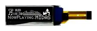
Graphic OLED, 128 x 32 Pixels, White on Black, 2.8V, SPI, 48mm x 11.5mm, -40 °C
- Manufacturer: MIDAS DISPLAYS
- Product type: Graphic OLED Displays
- Resolution:128 x 32 Pixels; Display Appearance:White on Black; Logic Voltage:2.8V; Interface Type:SPI; Module Size:48mm x 11.5mm; Operating Temperature Min:-40°C; Operating Temperature
- MSL: -
- SVHC: No SVHC (25-Jun-2025)
- Resolution: 128 x 32 Pixels
- Module Size: 48mm x 11.5mm
- Logic Voltage: 2.8V
- Product Range: -
- Interface Type: SPI
- Display Appearance: White on Black
- Display Construction: TAB
- Operating Temperature Max: 70°C
- Operating Temperature Min: -40°C
| Delivery and price | |
|---|---|
| Units per pack | 250 |
| Price | 7.93 € |
| Current stock | 10+ |
| Lead time | 30 days |
**Sauls Wharf House Crittens Road Great Yarmouth Norfolk NR31 0AG**

Telephone +44 (0)1493 602602 Email:sales@midasdisplays.com Email:tech@midasdisplays.com www.midasdisplays.com

|MCOT128032CY-WS|MCOT128032CY-WS|128 x 32|128 x 32|OLED Module|
|---|---|---|---|---|
|**Specification**|||||
|Version:    1|||Date: 10/12/2016||
|**Revision**|||||
|1|07/12/2016||First Issue||


|DisplayFeatures|DisplayFeatures|||
|---|---|---|---|
|Resolution|128 x 32|||
|Appearance|Whiteon Black|||
|Logic Voltage|2.8V|||
|Interface|SPI|||
|Module Size|48.00 x 11.50 x 1.40mm|||
|OperatingTemperature|-40°C ~ +80°C|BoxQuantity|Weight / Display|
|Construction|COT|---|---|


* - For full design functionality, please use this specification in conjunction with the SSD1306 specification. (Provided Separately)

|**Display Accessories**|**Display Accessories**|
|---|---|
|**Part Number**|**Description**|


|**Optional Variants**||
|---|---|
|**Appearance**|**Voltage**|


Page 1 of 15

## **`Basic Specifications`**

## Display Specifications

- 1) Display Mode : Passive Matrix

- 2) Display Color : Monochrome (white) 3) Drive Duty : 1/32 Duty

## Mechanical Specifications

- 1) Outline Drawing : According to the annexed outline drawing

- 2) Number of Pixels : 128 × 32

- 3) Module Size : 48.00 × 11.50 × 1.40 (mm)

- 4) Panel Size : 30.00 × 11.50 × 1.40 (mm)  including “Anti-Glare polarizer”

- 5) Active Area : 22.384 × 5.584 (mm)

- 6) Pixel Pitch : 0.175 × 0.175 (mm) 7) Pixel Size : 0.159 × 0.159 (mm) 8) Weight : TBD (g) ± 10%

## Active Area / Memory Mapping & Pixel Construction

**==> picture [390 x 230] intentionally omitted <==**

**----- Start of picture text -----**<br>
P0.175x128-0.016=22.384<br>Driver IC Memory Mapping<br>(128  x  32 in 128  x  64)<br>0.175<br>(0, 0) "A" 0.159<br>Segment 127 Segment 0 (127, 31)<br>(  Column 1  ) (  Column 128  )<br>Common 0<br>Detail "A"<br>(  Row 32  )<br>Scale (10:1)<br>Common 31<br>(  Row 1  )<br>0.175<br>P0.175x32-0.016=5.584 0.159<br>**----- End of picture text -----**<br>


Page 2 of 15

**==> picture [444 x 818] intentionally omitted <==**

**----- Start of picture text -----**<br>
i i : -0.0<br>ay<br>q<br>=}<br>|<br>s 4.84.07<br>S fj PO-3x(15-1)=4.220.05 3<br>g W=0.340.05<br>+<br>- os i)<br>2-G0.80.1 anc 4 ss |<br>(0.86) YU;4<br>SE 3 %<br>5 | A<br>o| x +<br>ose<br>7 00<br>pis 7 :<br>eel =<br>|<br>ss| i |<br>= 3 a | I ee ee<br>(2.1) ipa<br>(1.1) tL ee.594 cvia)<br>0,540.5 3 940.5 (Polarizer<br>11.5+0.2 (Cap Size)<br>11.540.2 (Panel Size)<br>Page 3 of 15<br>(Row 1)  (Row32)  Symbol  C2P  C2N CIP  CIN  VDDB vss  VDD  CS# RES# DIC# DO(SCI.K)  Dl(SDIN)  IREF VCOMH  vcc<br>ommon31  CommonO<br>r<br>Pin  I  2  3  4  5  6  7  8  9  10  11  12  13  14  15<br>SegmentO  Column 128)<br>(<br>□ 7 [<br>: 1)<br>li-- .0v·<br>□□□□□□□□□ Detail "A"  Scale (10<br>175-+--+<br>Segment 127  Column 1)  (  0 .159--.! ==I=  '°<br>0.<br>5: C:  --l---4p<br>+-2.5±0. 2<br>+--<br>Contact Side<br>-----18±0.3-------i<br>-----------------, ( 5)---<br>..i1<br>-+-+<br>- -+<br>--< 10)1--<br>+--<br>30±0.2 (Panel Size)- 24.384 (VIA)-------+ 22.384 (A/A)-<br>-25.9±0.5 (Polarizer)-<br>. m<br> with above materials should be 1.75 Max.<br>---------------148)1-- ----26.6±0.2 (Cap Size)------i<br>-i-------i---- t=<br>(2.1)<br>(1.1)  i--- $  t--<br> (1.5 Max) is without polarizer pr otective film & remove tape.<br>0.35±0.3--<br>embled total thicknes<br>Color:Driver IC: SSD1306  General Tolerance: ±0.30The total thicknesThe actual as<br>Notes:  1. 2. 3. Connector: HIROSE(HRS) FH26-1SS-0.3SHW(0S) Farnell: 2427760 or Equivalent) 4. Interface: 4-wire SPI 5. 6.<br>_<br>!::><br>=====t<br>•l<br>n=·ffi=<br>S<br>=±0=.=3(<br>3<br>**----- End of picture text -----**<br>


## Pin Definition

|Pin Definition||||
|---|---|---|---|
|Pin Number|Symbol|I/O|Function|
|**Power Supply**||||
|6<br>7<br>15|VSS<br>VDD<br>VCC|P<br>P<br>P|**Ground of OEL System**<br>This is a ground pin.  It also acts as a reference for the logic pins, the OEL driving<br>voltages, and the analog circuits.  It must be connected to external ground.<br>**Power Supply for Logic**<br>This is a voltage supply pin.  It must be connected to external source.<br>**Power Supply for OEL Panel**<br>This is the most positive voltage supply pin of the chip. A stabilization capacitor<br>should be connected between this pin and VSSwhen the converter is used.  It<br>must be connected to externalsourcewhenthe converter isnot used.|
|**Driver**||||
|13<br>14|IREF<br>VCOMH|I<br>O|**Current Reference for Brightness Adjustment**<br>This pin is segment current reference pin.  A resistor should be connected<br>between this pin and VSS.  Set the current at 12.5µA maximum.<br>**Voltage Output High Level for COM Signal**<br>This pin is the input pin for the voltage output high level for COM signals.<br>A capacitor should be connected between this pin and VSS.|
|**DC/DC Converter**||||
|1 / 2<br>3 / 4<br>5|C2P / C2N<br>C1P / C1N<br>VDDB|I<br>P|**Positive Terminal of the Flying Inverting Capacitor**<br>**Negative Terminal of the Flying Boost Capacitor**<br>The charge-pump capacitors are required between the terminals.  They must be<br>floated when the converter is not used.<br>**Power Supply for DC/DC Converter Circuit**<br>This is the power supply pin for the internal buffer of the DC/DC voltage converter.<br>It must be connected to external source when the converter is used.  It should be<br>connected toVDDwhenthe converter isnot used.|
|**Interface**||||
|8<br>9<br>10<br>11<br>12|CS#<br>RES#<br>D/C#<br>SCLK<br>SDIN|I<br>I<br>I<br>I<br>I|**Chip Select**<br>This pin is the chip select input.  The chip is enabled for MCU communication only<br>when CS# is pulled low.<br>**Power Reset for Controller and Driver**<br>This pin is reset signal input.  When the pin is low, initialization of the chip is<br>executed.<br>**Data/Command Control**<br>This pin is Data/Command control pin.  When the pin is pulled high, the data at<br>SDIN is treated as data.  When it is pulled low, the data at SDIN will be<br>transferred to the command register.  For detail relationship to MCU interface<br>signals, please refer to the Timing Characteristics Diagrams.<br>**Serial Clock Input Signal**<br>The transmission of information in the bus is following a clock signal.  Each<br>transmission of data bit is taken place during a single clock period of this pin.<br>**Serial Data Input Signal**<br>This pin acts as a communication channel.  The input data through SDIN are<br>latched at the rising edge of SCLK in the sequence of MSB first and converted to<br>8-bit parallel data and handled at the rising edge of last serial clock.<br>SDIN is identified to display data or command by D/C# bit data at the rising of first<br>SCLK.|


Page 4 of 15

## **`Absolute Maximum Ratings`**

|Parameter|Symbol|Min|Max|Unit|Notes|
|---|---|---|---|---|---|
|Supply Voltage for Logic<br>Supply Voltage for Display<br>Supply Voltage for DC/DC<br>Operating Temperature<br>Storage Temperature<br>Lifetime(70 nits) (Typ)30K                                                hour           4|VDD<br>VCC<br>VDDB<br>TOP<br>TSTG<br>30K                                                hour           4|-0.3<br>0<br>-0.3<br>-40<br>-40<br>30K                                                hour           4|4<br>11<br>5<br>70<br>85<br>30K                                                hour           4|V<br>V<br>V<br>°C<br>°C<br>30K                                                hour           4|1, 2<br>1, 2<br>1, 2<br>3<br>30K                                                hour           4|


Note 1: All the above voltages are on the basis of “V `SS` = 0V”.

- Note 2: When this module is used beyond the above absolute maximum ratings, permanent breakage of the module may occur.  Also, for normal operations, it is desirable to use this module under the conditions according to Section 3. “Optics & Electrical Characteristics”.  If this module is used beyond these conditions, malfunctioning of the module can occur and the reliability of the module may deteriorate.

- Note 3: The defined temperature ranges do not include the polarizer. The maximum withstood temperature of the polarizer should be 80 ° C.

- Note 4: End of lifetime is specified as 50% of initial brightness reached. The reference average operation life time at room temperature is estimated by the accelerated at high temperature conditions.

Page 5 of 15

## **`Optics & Electrical Characteristics`**

## Optics Characteristics

|Optics Characteristics|||||||
|---|---|---|---|---|---|---|
|Characteristics|Symbol|Conditions|Min|Typ|Max|Unit|
|Brightness<br>C.I.E. (White)<br>Dark Room Contrast<br>Viewing Angle|Lbr<br>(x)<br>(y)<br>CR|Note 5<br>C.I.E. 1931|120<br>0.25<br>0.27<br>-<br>-|150<br>0.29<br>0.31<br>>10,000:1<br>Free|-<br>0.33<br>0.35<br>-<br>-|cd/m2<br>degree|


* Optical measurement taken at V `DD` = 2.8V, V `CC` = 7.5V. Software configuration follows Section 4.5 Initialization.

## DC Characteristics

V `CC` Supplied Externally

|Characteristics|Symbol|Conditions|Min|Typ|Max|Unit|
|---|---|---|---|---|---|---|
|Supply Voltage for Logic<br>Supply Voltage for Display<br>(Supplied Externally)<br>High Level Input<br>Low Level Input<br>High Level Output<br>Low Level Output<br>Operating Current for VDD<br>Operating Current for VCC<br>(VCCSupplied Externally)<br>Sleep Mode Current for VDD<br>Sleep Mode Current for VCC|VDD<br>VCC<br>VIH<br>VIL<br>VOH<br>VOL<br>IDD<br>ICC<br>IDD, SLEEP<br>ICC, SLEEP|Note 5<br>(Internal DC/DC Disable)<br>IOUT= 100µA, 3.3MHz <br>IOUT= 100µA, 3.3MHz<br>Note 6<br>Note 7<br>Note 8|1.65<br>7.0<br>0.8×VDD<br>0<br> 0.9×VDD<br>0<br>-<br>-<br>-<br>-<br>-<br>-|2.8<br>7.5<br>-<br>-<br>-<br>-<br>180<br>2.8<br>4.4<br>8.2<br>1<br>2|3.3<br>8.0<br>VDD<br>0.2×VDD<br>VDD<br>0.1×VDD<br>300<br>3.5<br>5.5<br>10.3<br>5<br>10|V<br>V<br>V<br>V<br>V<br>V<br>µA<br>mA<br>mA<br>mA<br>µA<br>µA|


Note 5: Brightness (L `br` ) and Supply Voltage for Display (V `CC` ) are subject to the change of the panel characteristics and the customer’s request.

Note 6: V `DD` = 2.8V, V `CC` = 7.5V, 30% Display Area Turn on.

Note 7: V `DD` = 2.8V, V `CC` = 7.5V, 50% Display Area Turn on. Note 8: V `DD` = 2.8V, V `CC` = 7.5V, 100% Display Area Turn on.

* Software configuration follows Section 4.5.1 Initialization.

Page 6 of 15

## 3.2.2 V `CC` Generated by Internal DC/DC Circuit

|Characteristics|Symbol|Conditions|Min|Typ|Max|Unit|
|---|---|---|---|---|---|---|
|Supply Voltage for Logic<br>Supply Voltage for DC/DC<br>Supply Voltage for Display<br>(Generated by Internal DC/DC)<br>High Level Input<br>Low Level Input<br>High Level Output<br>Low Level Output<br>Operating Current for VDD<br>Operating Current for VDDB<br>(VCCGenerated by Internal DC/DC)<br>Sleep Mode Current for VDD<br>Sleep Mode Current for VCC|VDD<br>VDDB<br>VCC<br>VIH<br>VIL<br>VOH<br>VOL<br>IDD<br>IDDB<br>IDD, SLEEP<br>ICC, SLEEP|Internal DC/DC Enable<br>Note 9<br>(Internal DC/DC Enable)<br>IOUT= 100µA, 3.3MHz <br>IOUT= 100µA, 3.3MHz<br>Note 10<br>Note 11<br>Note 12|1.65<br>3.0<br>7.0<br>0.8×VDD<br>0<br> 0.9×VDD<br>0<br>-<br>-<br>-<br>-<br>-<br>-|2.8<br>-<br>7.5<br>-<br>-<br>-<br>-<br>180<br>7.8<br>12.2<br>22.1<br>1<br>2|3.3<br>4.2<br>8.0<br>VDD<br>0.2×VDD<br>VDD<br>0.1×VDD<br>300<br>9.8<br>15.3<br>27.6<br>5<br>10|V<br>V<br>V<br>V<br>V<br>V<br>V<br>µA<br>mA<br>mA<br>mA<br>µA<br>µA|


Note 9: Brightness (L `br` ) and Supply Voltage for Display (V `CC` ) are subject to the change of the panel characteristics and the customer’s request.

Note 10: V `DD` = 2.8V, V `DDB` = 3.5V, V `CC` Generated by Internal DC/DC Circuit, 30% Display Area Turn on. Note 11: V `DD` = 2.8V, V `DDB` = 3.5V, V `CC` Generated by Internal DC/DC Circuit, 50% Display Area Turn on. Note 12: V `DD` = 2.8V, V `DDB` = 3.5V, V `CC` Generated by Internal DC/DC Circuit, 100% Display Area Turn on.

* Software configuration follows Section 4.5.2 Initialization.

Page 7 of 15

## AC Characteristics

|Symbol|Description|Min|Max|Unit|
|---|---|---|---|---|
|tcycle<br>tAS<br>tAH<br>tCSS<br>tCSH<br>tDSW<br>tDHW<br>tCLKL<br>tCLKH<br>tR<br>tF|Clock Cycle Time<br>Address Setup Time<br>Address Hold Time<br>Chip Select Setup Time<br>Chip Select Hold Time<br>Write Data Setup Time<br>Write Data Hold Time<br>Clock Low Time<br>Clock High Time<br>Rise Time<br>Fall Time|100<br>15<br>15<br>20<br>10<br>15<br>15<br>20<br>20<br>-<br>-|-<br>-<br>-<br>-<br>-<br>-<br>-<br>-<br>-<br>40<br>40|ns<br>ns<br>ns<br>ns<br>ns<br>ns<br>ns<br>ns<br>ns<br>ns<br>ns|


* (V `DD` - V `SS` = 1.65V to 3.3V, T `a` = 25°C)

Page 8 of 15

## **`Functional Specification`**

## Commands

Refer to the Technical Manual for the SSD1306

## Power down and Power up Sequence

To protect OEL panel and extend the panel life time, the driver IC power up/down routine should include a delay period between high voltage and low voltage power sources during turn on/off.  It gives the OEL panel enough time to complete the action of charge and discharge before/after the operation.

## 4.2.1 Power up Sequence:

   1. Power up V `DD` / V `DDB`

   2. Send Display off command

   3. Initialization

   4. Clear Screen

   5. Power up V `CC`

   6. Delay 100ms (When V `CC` is stable)

   7. Send Display on command

- 4.2.2 Power down Sequence:

   1. Send Display off command

   2. Power down V `CC` / V `DDB`

   3. Delay 100ms (When V `CC` / V `DDB` is reach 0 and panel is completely discharges)

   4. Power down V `DD`

**==> picture [165 x 208] intentionally omitted <==**

**----- Start of picture text -----**<br>
V [B] DD B / V B DDB B on<br>V [B] CC B on<br>Display on<br>VB CC<br>VB DD /VB DDB<br>VB SS B/Ground<br>Display off<br>V [B] CC B / V B DDB off<br>V [B] DD B off<br>VB CC /VB DDB<br>VB DD<br>VB SS B/Ground<br>**----- End of picture text -----**<br>


Note 9:

- 1) Since an ESD protection circuit is connected between V `DD` and V `CC` inside the driver IC, V `CC` becomes lower than V `DD` whenever V `DD` is ON and V `CC` is OFF.

- 2) V `CC` / V `DDB` should be kept float (disable) when it is OFF.

- 3) Power Pins (V `DD` , V `CC` , V `DDB` ) can never be pulled to ground under any circumstance.

- 4) V `DD` should not be power down before V `CC` / V `DDB` power down.

## Reset Circuit

When RES# input is low, the chip is initialized with the following status:

1. Display is OFF

2. 128 × 64 Display Mode

3. Normal segment and display data column and row address mapping (SEG0 mapped to column address 00h and COM0 mapped to row address 00h)

4. Shift register data clear in serial interface

5. Display start line is set at display RAM address 0

6. Column address counter is set at 0

7. Normal scan direction of the COM outputs

8. Contrast control register is set at 7Fh

9. Normal display mode (Equivalent to A4h command)

Page 9 of 15

## Application Circuit

V `CC` Supplied Externally

Page 10 of 15

V `CC` Generated by Internal DC/DC Circuit

Page 11 of 15

## Actual Application Example

Command usage and explanation of an actual example

## 4.5.1 V `CC` Supplied Externally

<Power up Sequence>

**==> picture [381 x 336] intentionally omitted <==**

**----- Start of picture text -----**<br>
Set Multiplex Ratio Set Pre-Charge Period<br>V DD /V CC  off State<br>0xA8, 0x1F  0xD9, 0x22<br>Power up VDD Set Display Offset Set VCOMH Deselect Level<br>(RES# as Low State)  0xD3, 0x00  0xDB, 0x30<br>Power Stabilized Set Display Start Line Set Entire Display On/Off<br>(Delay Recommended)  0x40  0xA4<br>Set RES# as High Set Charge Pump Set Normal/Inverse Display<br>(3µs Delay Minimum)  0x8D, 0x10  0xA6<br>Initialized State Set Segment Re-Map<br>Clear Screen<br>(Parameters as Default)  0xA1<br>Set Display Off Set COM Output Scan Direction Power up VCC<br>0xAE  0xC8  (100ms Delay Recommended)<br>Initial Settings  Set COM Pins Hardware Configuration Set Display On<br>Configuration  0xDA, 0x02  0xAF<br>Set Display Clock Divide Ratio/Oscillator Frequency Set Contrast Control<br>Display Data Sent<br>0xD5, 0x80  0x81, 0x9F<br>**----- End of picture text -----**<br>


If the noise is accidentally occurred at the displaying window during the operation, please reset the display in order to recover the display function.

<Power down Sequence>

**==> picture [347 x 63] intentionally omitted <==**

**----- Start of picture text -----**<br>
Normal Operation Power down V B CC B  V DD /V CC  off State<br>(100ms Delay Recommended)<br>Set Display Off<br>0xAE  Power down VDD<br>**----- End of picture text -----**<br>


Page 12 of 15

<Entering Sleep Mode>

**==> picture [259 x 261] intentionally omitted <==**

**----- Start of picture text -----**<br>
Normal Operation Power down VCC<br>Set Display Off<br>Sleep Mode<br>0xAE<br>a<br><Exiting Sleep Mode><br>Set Display On<br>Sleep Mode<br>0xAF<br>Power up VCC<br>Normal Operation<br>(100ms Delay Recommended)<br>=<br>**----- End of picture text -----**<br>


<Exiting Sleep Mode>

Page 13 of 15

## 4.5.2 V `CC` Generated by Internal DC/DC Circuit

<Power up Sequence>

**==> picture [377 x 336] intentionally omitted <==**

**----- Start of picture text -----**<br>
Set Display Clock Divide Ratio/Oscillator Frequency Set Contrast Control<br>V DD /V DDB  off State<br>0xD5, 0x80 0x81, 0x82<br>Power up VDD Set Multiplex Ratio Set Pre-Charge Period<br>(RES# as Low State)  0xA8, 0x1F 0xD9, 0xF1<br>Power Stabilized Set Display Offset Set VCOMH Deselect Level<br>(Delay Recommended)  0xD3, 0x00  0xDB, 0x30<br>Power up VDDB Set Display Start Line Set Entire Display On/Off<br>(100ms Delay Recommended) 0x40 0xA4<br>Set RES# as High Set Charge Pump Set Normal/Inverse Display<br>(3µs Delay Minimum) 0x8D,  0x14 0xA6<br>Initialized State Set Segment Re-Map<br>Clear Screen<br>(Parameters as Default) 0xA1<br>Set Display Off Set COM Output Scan Direction Set Display On<br>0xAE 0xC8 0xAF<br>Initial Settings  Set COM Pins Hardware Configuration<br>Display Data Sent<br>Configuration 0xDA, 0x02<br>**----- End of picture text -----**<br>


If the noise is accidentally occurred at the displaying window during the operation, please reset the display in order to recover the display function.

<Power down Sequence>

**==> picture [347 x 109] intentionally omitted <==**

**----- Start of picture text -----**<br>
Power Stabilized<br>Normal Operation V DD /V DDB  off State<br>(100ms Delay Recommended)<br>Set Display Off Power down V B DDB<br>0xAE (50ms Delay Recommended)<br>Set Charge Pump<br>0x8D, 0x10 Power down VDD<br>**----- End of picture text -----**<br>


Page 14 of 15

<Entering Sleep Mode>

**==> picture [417 x 261] intentionally omitted <==**

**----- Start of picture text -----**<br>
Set Charge Pump<br>Normal Operation Sleep Mode<br>0x8D, 0x10<br>Set Display Off<br>0xAE Power down VDDB<br>=SS —<br><Exiting Sleep Mode><br>Set Charge Pump<br>Sleep Mode Normal Operation<br>0x8D,  0x14<br>Power up VDDB Set Display On<br>(100ms Delay Recommended) 0xAF<br>=i<br>**----- End of picture text -----**<br>


Page 15 of 15
Updated at April 27, 2026
Midas Displays is a recognized specialist in the electronic display industry, dedicated to providing high-quality visual solutions tailored to a wide range of applications. Backed by a UK-based, in-house team of engineers, the company is known for its extensive technical knowledge and commitment to delivering fast, reliable service. This expertise ensures that designers and manufacturers receive best-in-class support when integrating displays into their projects. The core of the Midas Displays portfolio features an extensive selection of Liquid Crystal Displays (LCD). Ranging from standard character and graphic modules to advanced configurations, these LCD displays are engineered for exceptional clarity and durability. Designed to meet the rigorous demands of various industries, they provide reliable performance for both industrial and commercial applications requiring robust and cost-effective visual output. Complementing their primary LCD offerings, Midas Displays also provides a versatile range of Organic Light Emitting Diode (OLED) displays. These advanced modules deliver high-contrast, energy-efficient viewing solutions ideal for modern, compact electronic designs. To ensure seamless integration across all display types, the company supports its core products with a variety of complementary accessories, including touch screens, interconnects, and evaluation kits.
About Novapart
Novapart is a B2B electronic component broker specialising in stock shortages and cost reduction. We source hard-to-find parts and identify compliant alternatives across a catalogue of 410,000+ components from 500+ manufacturers.
Learn more →Stock Shortage Specialist
When a component is unavailable, discontinued or has an unacceptable lead time, we tap into our network of vetted European and Asian distributors to source what you need — without compromising on quality or traceability.
Request a quote →Compliant Alternatives
We identify pin-to-pin, electrically equivalent substitutes that meet the same certifications (RoHS, AEC-Q100, REACH) as your original specification — validated against datasheets, not just part numbers. Often at a lower cost.
BOM Analysis service →