
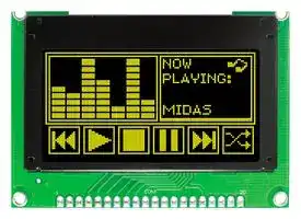


MCOB128064T1V-YP
Graphic OLED, 128 x 64 Pixels, Yellow on Black, 3V, Parallel, 75mm x 52.7mm, -40 °C
- Manufacturer: MIDAS DISPLAYS
- Product type: Graphic OLED Displays
- Resolution:128 x 64 Pixels; Display Appearance:Yellow on Black; Logic Voltage:3V; Interface Type:Parallel; Module Size:75mm x 52.7mm; Operating Temperature Min:-40°C; Operating Temperat
- MSL: -
- SVHC: No SVHC (25-Jun-2025)
- Resolution: 128 x 64 Pixels
- Module Size: 75mm x 52.7mm
- Logic Voltage: 3V
- Product Range: -
- Interface Type: Parallel
- Display Appearance: Yellow on Black
- Display Construction: COB
- Operating Temperature Max: 80°C
- Operating Temperature Min: -40°C
| Delivery and price | |
|---|---|
| Units per pack | 100 |
| Price | 23.94 € |
| Current stock | 10+ |
| Lead time | 30 days |
**Sauls Wharf House Crittens Road Great Yarmouth Norfolk NR31 0AG**

Telephone +44 (0)1493 602602 Email:sales@midasdisplays.com Email:tech@midasdisplays.com www.midasdisplays.com

|MCOB128064T1V-YP|MCOB128064T1V-YP|128 x 64|128 x 64|OLED Module|
|---|---|---|---|---|
|**Specification**|||||
|Version:    1|||Date:01/12/2017||
|**Revision**|||||
|1|29/11/2017||First Issue||


|DisplayFeatures|DisplayFeatures|||
|---|---|---|---|
|Resolution|128 x 64|||
|Appearance|Yellow on Black|||
|Logic Voltage|3V|||
|Interface|Parallel|||
|Module Size|75.00 x 52.70 x 8.50mm|||
|OperatingTemperature|-40°C ~ +80°C|BoxQuantity|Weight / Display|
|Construction|COB|---|---|


* - For full design functionality, please use this specification in conjunction with the SSD1309 specification. (Provided Separately)

|**Display Accessories**|**Display Accessories**|
|---|---|
|**Part Number**|**Description**|
|MCC1A20DILP<br>-20DILS-150|20 Way Dual in-line to Dual in-line<br>connector cable.|
|VBWFD2|USB PIC18F2550 micro-<br>controller board to 20 Way DIL<br>COB graphic LCD.|
|||


|**Optional Variants**||
|---|---|
|**Appearance**|**Voltage**|


Page 1 of 15

## **General Specification**

The Features is described as follow:

- Module dimension: 75.0 × 52.7 × 8.5 mm

- Active area: 55.01 × 27.49mm

- Dot Matrix: 128*64

- Pixel Size: 0.40 × 0.40 mm

- Pixel Pitch: 0.43 × 0.43 mm

- Display Mode:Passive Matrix

- Duty: 1/64 Duty

- Display Color: Monochrome (Yellow)

- Controller IC: SSD1309

- Interface: 8080

- SIZE: 2.42inch

## **Interface Pin Function**

|**No.**|**Symbol Function**|**mbol Function**|
|---|---|---|
|1|VDD|Power supply pin for core logic operation.|
|2|VSS|Ground.|
|3|NC|No connection|
|4~11|D0~D7|Data bus.|
|12|CS|This pin is the chip select input connecting to the MCU.<br>The chip is enabled for MCU communication only when CS# is pulled<br>LOW (active LOW).|
|13|NC|No connection|
|14|/RES|This pin is reset signal input.<br>When the pin is pulled LOW, initialization of the chip is executed.<br>Keep this pin pull HIGH during normal operation.|
|15|R/W|This pin is read / write control input pin connecting to the MCU<br>interface.<br>When 8080 interface mode is selected,this pin is pulled LOW and the<br>chip is selected|
|16|D/C|This pin is Data/Command control pin connecting to the MCU.|
|17|E|This pin is MCU interface input.<br>When 8080 interface mode is selected, this pin is pulled LOW and the<br>chip is selected|
|18|NC|No connection|
|19|DISP|Displayoff|
|20|NC|No connection|


- 80 Series Interface is default

Page 2 of 15

## **Contour Drawing & Block Diagram**

## **FUNCTION BLOCK DIAGRAM**

*For more information, please refer to Application Note provided by Midas Displays.

Page 3 of 15

## **Absolute Maximum Ratings**

|**Parameter**|**Symbol**|**Min**|**Max**|**Unit**|**Notes**|
|---|---|---|---|---|---|
|Supply Voltage for Logic|VDD|-0.3|4|V||
|Operating Temperature|TOP|-40|+80|°C|-|
|Storage Temperature|TSTG|-40|+85|°C|-|


Maximum ratings are those values beyond which damages to the device may occur. Functional operation should be restricted to the limits in the Electrical Characteristics tables or Pin Description section.

This device may be light sensitive. Caution should be taken to avoid exposure of this device to any light source during normal operation. This device is not radiation protected.

## **Electrical Characteristics**

|**Item**|**Symbol**|**Condition**|**Min**|**Typ**|**Max**|**Unit**|
|---|---|---|---|---|---|---|
|Supply Voltage for Logic|VDD|-|2.8|3.0|3.3|V|
|High Level Input|VIH|-|0.8×VDD|0.8×VDD<br>-|-|V|
|Low Level Input|VIL|-|-|-|0.2×VDD|0.2×VDD<br>V|
|High Level Output|VOH|-|0.9×VDD|0.9×VDD<br>-|-|V|
|Low Level Output|VOL|-|-|-|0.1×VDD|0.1×VDD<br>V|
|50% Check Board<br>operating Current|IDD|VDD =3.0V|130|135|150|mA|


Page 4 of 15

## **Optical Characteristics**

|**Item**|**Symbol**|**Condition**|**Min**|**Typ**|**Max**|**Unit**|
|---|---|---|---|---|---|---|
|View Angle|(V)θ|-|160|-|-|deg|
||(H)φ|-|160|-|-|deg|
|Contrast Ratio|CR|Dark|2000:1|-|-|-|
|Response Time|T rise|-|-|10|-|μs|
||T fall|-|-|10|-|μs|
|Display with 50% check Board Brightness|||80|100|-|-|
|CIEx(Yellow)||x,y(CIE1931)|0.45|0.47|0.49|-|
|CIEy(Yellow)||x,y(CIE1931)|0.48|0.50|0.52|-|


## **OLED Lifetime**

|ITEM|Conditions|Min|Typ|Remark|
|---|---|---|---|---|
|Operating<br>Life Time|Ta=25℃<br>/ Initial 50% check board<br>brightness Typical Value|50,000 Hrs|-|Note|


## Notes:

1. Life time is defined the amount of time when the luminance has decayed to <50% of the initial value.

2. This analysis method uses life data obtained under accelerated conditions to extrapolate an estimated probability density function ( _pdf_ ) for the product under normal use conditions.

3. Screen saving mode will extend OLED lifetime.

Page 5 of 15

## **Reliability**

## **Content of Reliability Test**

|**Contentntenttentntt of Reliability Testf Reliability Testeliability Testliability Testability Testility Testty Test Testest**|**Contentntenttentntt of Reliability Testf Reliability Testeliability Testliability Testability Testility Testty Test Testest**|**Contentntenttentntt of Reliability Testf Reliability Testeliability Testliability Testability Testility Testty Test Testest**|**Contentntenttentntt of Reliability Testf Reliability Testeliability Testliability Testability Testility Testty Test Testest**|**Contentntenttentntt of Reliability Testf Reliability Testeliability Testliability Testability Testility Testty Test Testest**|
|---|---|---|---|---|
|**Environmental Test**|||||
|**Test Item**|**Content of Test**|**Test Condition**|**Applicable**<br>**Standard**||
|High<br>Temperature<br>storage|Endurance test applying the high<br>storage temperature for a long time.|85℃<br>240hrs|——||
|Low<br>Temperature<br>storage|Endurance test applying the low storage<br>temperature for a long time.|Endurance test applying the low storage<br>-40℃<br>240hrs|——||
|High<br>Temperature<br>Operation|Endurance test applying the electric<br>stress (Voltage & Current) and the<br>thermal stress to the element for a long<br>time.|80℃<br>240hrs|——||
|Low<br>Temperature<br>Operation|Endurance test applying the electric<br>stress under low temperature for a long<br>time.|-40℃<br>240hrs|——||
|High<br>Temperature/<br>Humidity<br>Storage|Endurance test applying the high<br>temperature and high humidity storage<br>for a long time.|60℃,90%RH<br>240hrs|——||
|High<br>Temperature/<br>Humidity<br>Operation|Endurance test applying the high<br>temperature and high humidity<br>Operation for a long time.|60℃,90%RH<br>120hrs|||
|Temperature<br>Cycle|Endurance test applying the low and<br>high temperature cycle.<br>-40℃25℃80℃<br>30min    5min     30min<br>1cycle|-40℃/80℃<br>30 cycles|——||
|Mechanical Test|||||
|Vibration test|Endurance test applying the vibration<br>during transportation and using.|Frequency:10~55Hz<br>amplitude:1.5mm<br>Time:0.5hrs/axis<br>Test axis:X,Y,Z|——||
|Others|||||
|Static<br>electricity test|Endurance test applying the electric<br>stress to the terminal.|Air Discharge model<br>±4kv,10 times||——|


*** Supply voltage for OLED system =Operating voltage at 25 ℃

Page 6 of 15

## **Test and measurement conditions**

1. All measurements shall not be started until the specimens attain to temperature stability. After the completion of the described reliability test, the samples were left at room temperature for 2 hrs prior to conducting the failure test at 23±5°C; 55±15% RH.

2. All-pixels-on is used as operation test pattern.

3. The degradation of Polarizer are ignored for High Temperature storage, High Temperature/ Humidity Storage, Temperature Cycle

## **Evaluation criteria**

1. The function test is OK.

2. No observable defects.

3. Luminance: > 50% of initial value.

4. Current consumption: within ± 50% of initial value.

## **APPENDIX:**

## **RESIDUE IMAGE**

Because the pixels are lighted in different time, the luminance of active pixels may reduce or differ from inactive pixels. Therefore, the residue image will occur. To avoid the residue image, every pixel needs to be lighted up uniformly.

Page 7 of 15

**Inspection specification**

NO Item Criterion AQL 01 Electrical 1.1 Missing vertical, horizontal segment, segment contrast Testing defect. 1.2 Missing character , dot or icon. 1.3 Display malfunction. 1.4 No function or no display. 0.65 1.5 Current consumption exceeds product specifications. 1.6 OLED viewing angle defect. 1.7 Mixed product types. 1.8 Contrast defect. ~~al~~ 02 Black or 2.1 White and black spots on display ≦ 0.25mm, no more than white three white or black spots present. spots on 2.2 Densely spaced: No more than two spots or lines within 2.5 OLED 3mm. (display only) 03 OLED 3.1 Round type : As black following drawing SIZE Acceptable Q ~~r~~ spots, Φ=( x + y ) / 2 ~~e~~ TY white Φ ≦ 0.10 Accept no spots, dense contamina 0.10 < 2 2.5 tion Φ ≦ 0.20 (non-displ 0.20 < 1 ay) Φ ≦ 0.25 0.25 < Φ 0 im ~~==|~~ 3.2 Line type : (As following drawing) Length Width Acceptable Q TY --W ≦ 0.02 Accept no dense L ≦ 3.0 0.02 < W ≦ 0.03 2.5 2 L ≦ 2.5 0.03 < W ≦ 0.05 --0.05 < W As round type ~~PES~~ 04 Polarizer bubbles If bubbles are visible, Size Φ Acceptable Q TY judge using black spot Φ ≦ 0.20 Accept no dense specifications, not easy 0.20 < Φ ≦ 0.50 3 2.5 to find, must check in 0.50 < Φ ≦ 1.00 2 specify direction. 1.00 < Φ 0 Total Q TY 3 ~~TT ==~~ Page 8 of 15

|NO<br>~~a~~|Item|Criterion|AQL|
|---|---|---|---|
|05<br>~~a~~|Scratches|Follow NO.3 OLED black spots, white spots, contamination||
|06|Chipped<br>glass|Symbols Define:<br>x: Chip length      y: Chip width     z: Chip thickness<br>k: Seal width       t: Glass thickness  a: OLED side length<br>L: Electrode pad length:<br>6.1 General glass chip :<br>6.1.1 Chip on panel surface and crack between panels:<br>z: Chip thickness<br>y: Chip width<br>x: Chip length<br>Z≦1/2t<br>Not over viewing<br>area<br>x≦1/8a<br>1/2t<z≦2t<br>Not exceed 1/3k<br>x≦1/8a<br>☉If there are 2 or more chips, x is total length of each chip.<br>6.1.2 Corner crack:<br>z: Chip thickness<br>y: Chip width<br>x: Chip length<br>Z≦1/2t<br>Not over viewing<br>area<br>x≦1/8a<br>1/2t<z≦2t<br>Not exceed 1/3k<br>x≦1/8a<br>☉If there are 2 or more chips, x is the total length of each chip.|2.5|


Page 9 of 15

**==> picture [475 x 510] intentionally omitted <==**

**----- Start of picture text -----**<br>
a NO Item  Criterion  AQL<br>Symbols :<br>x: Chip length      y: Chip width     z: Chip thickness<br>k: Seal width       t: Glass thickness  a: OLED side length<br>L: Electrode pad length<br>6.2 Protrusion over terminal :<br>6.2.1 Chip on electrode pad :<br>Z<br>y: Chip width   x: Chip length  z: Chip thickness<br>y ≦ 0.5mm  x ≦ 1/8a  0  <  z  ≦  t<br>6.2.2 Non-conductive portion:<br>3 L<br>Glass<br>06  2.5<br>crack<br>x X<br>y: Chip width   x: Chip length  z: Chip<br>thickness<br>y ≦  L  x ≦ 1/8a  0  <  z  ≦  t<br>☉ If the chipped area touches the ITO terminal, over 2/3 of the ITO<br>must remain and be inspected according to electrode terminal<br>specifications.<br>☉ If the product will be heat sealed by the customer, the alignment<br>mark not be damaged.<br>6.2.3 Substrate protuberance and internal crack.<br>x<br>y: width   x: length<br>——— y ≦ 1/3L  x  ≦  a<br>**----- End of picture text -----**<br>


Page 10 of 15

|NO|Item|Criterion|AQL|
|---|---|---|---|
|07|Cracked<br>glass|The OLED with extensive crack is not acceptable.|2.5|
|08|Backlight<br>elements|8.1 Illumination source flickers when lit.<br>8.2 Spots or scratched that appear when lit must be judged.<br>Using OLED spot, lines and contamination standards.<br>8.3 Backlight doesn’t light or color wrong.|0.65<br>2.5<br>0.65|
|09|Bezel|9.1 Bezel may not have rust, be deformed or have<br>fingerprints, stains or other contamination.<br>9.2 Bezel must comply with job specifications.|2.5<br>0.65|
|10|PCB、COB|10.1 COB seal may not have pinholes larger than 0.2mm or<br>contamination.<br>10.2 COB seal surface may not have pinholes through to the<br>IC.<br>10.3 The height of the COB should not exceed the height<br>indicated in the assembly diagram.<br>10.4 There may not be more than 2mm of sealant outside the<br>seal area on the PCB. And there should be no more than<br>three places.<br>10.5 No oxidation or contamination PCB terminals.<br>10.6 Parts on PCB must be the same as on the production<br>characteristic chart. There should be no wrong parts,<br>missing parts or excess parts.<br>10.7 The jumper on the PCB should conform to the product<br>characteristic chart.<br>10.8 If solder gets on bezel tab pads, OLED pad, zebra pad<br>or screw hold pad, make sure it is smoothed down.|2.5<br>2.5<br>0.65<br>2.5<br>2.5<br>0.65<br>0.65<br>2.5|
|11|Soldering|11.1 No un-melted solder paste may be present on the PCB.<br>11.2 No cold solder joints, missing solder connections,<br>oxidation or icicle.<br>11.3 No residue or solder balls on PCB.<br>11.4 No short circuits in components on PCB.|2.5<br>2.5<br>2.5<br>0.65|


Page 11 of 15

|NO|Item|Criterion|AQL|
|---|---|---|---|
|12|General<br>appearance|12.1 No oxidation, contamination, curves or, bends on<br>interface Pin (OLB) of TCP.<br>12.2 No cracks on interface pin (OLB) of TCP.<br>12.3 No contamination, solder residue or solder balls on<br>product.<br>12.4 The IC on the TCP may not be damaged, circuits.<br>12.5 The uppermost edge of the protective strip on the<br>interface pin must be present or look as if it cause the<br>interface pin to sever.<br>12.6 The residual rosin or tin oil of soldering (component or<br>chip component) is not burned into brown or black color.<br>12.7 Sealant on top of the ITO circuit has not hardened.<br>12.8 Pin type must match type in specification sheet.<br>12.9 OLED pin loose or missing pins.<br>12.10 Product packaging must the same as specified on<br>packaging specification sheet.<br>12.11 Product dimension and structure must conform to<br>product specification sheet.|2.5<br>0.65<br>2.5<br>2.5<br>2.5<br>2.5<br>2.5<br>0.65<br>0.65<br>0.65<br>0.65|


Page 12 of 15

**==> picture [358 x 546] intentionally omitted <==**

**----- Start of picture text -----**<br>
Check Item  Classification  Criteria<br>No Display  Major<br>Missing Line<br>Major<br>(8<br>Pixel Short  Major<br>EERE<br>\Serceaeauea ae) | |<br>Darker Short  Major<br>aie<br>; -<br>|<br>Wrong Display  Major<br>fi<br>i<br>Un-uniform<br>B/A x 100% < 70%  Major<br>A/C x 100% < 70%<br>**----- End of picture text -----**<br>


Page 13 of 15

## **Precautions in use of OLED Modules**

(1) Avoid applying excessive shocks to module or making any alterations or modifications to it. (2) Don’t make extra holes on the printed circuit board, modify its shape or change the components of OLED display module.

(3) Don’t disassemble the OLED display module.

- (4) Don’t operate it above the absolute maximum rating.

(5) Don’t drop, bend or twist OLED display module.

(6) Soldering: only to the I/O terminals.

- (7) Storage: please storage in anti-static electricity container and clean environment.

(8) It's pretty common to use "Screen Saver" to extend the lifetime and Don't use fix information for long time in real application.

(9) Don't use fixed information in OLED panel for long time, that will extend "screen burn" effect time..

(10) Midas has the right to change the passive components, including R2and R3 adjust resistors.  (Resistors, capacitors and other passive components will have different appearance and color caused by the different supplier.)

(11) Midas have the right to change the PCB Rev. (In order to satisfy the supplying stability, management optimization and the best product performance...etc, under the premise of not affecting the electrical characteristics and external dimensions, Midas have the right to modify the version.)

## **Handling Precautions**

- (1) Since the display panel is being made of glass, do not apply mechanical impacts such us dropping from a high position.

- (2) If the display panel is broken by some accident and the internal organic substance leaks out, be careful not to inhale nor lick the organic substance.

- (3) If pressure is applied to the display surface or its neighborhood of the OLED display module, the cell structure may be damaged and be careful not to apply pressure to these sections.

- (4) The polarizer covering the surface of the OLED display module is soft and easily scratched. Please be careful when handling the OLED display module.

- (5) When the surface of the polarizer of the OLED display module has soil, clean the surface. It takes advantage of by using following adhesion tape.

- Scotch Mending Tape No. 810 or an equivalent

Never try to breathe upon the soiled surface nor wipe the surface using cloth containing solvent Also, pay attention that the following liquid and solvent may spoil the polarizer:

- Water

- Ketone

- Aromatic Solvents

- (6) Hold OLED display module very carefully when placing OLED display module into the System housing. Do not apply excessive stress or pressure to OLED display module. And, do not over bend the film with electrode pattern layouts. These stresses will influence the display performance. Also, secure sufficient rigidity for the outer cases.

Page 14 of 15

- (7) Do not apply stress to the LSI chips and the surrounding molded sections.

- (8) Do not disassemble nor modify the OLED display module.

- (9) Do not apply input signals while the logic power is off.

- (10) Pay sufficient attention to the working environments when handing OLED display modules to prevent occurrence of element breakage accidents by static electricity.

- Be sure to make human body grounding when handling OLED display modules.

- Be sure to ground tools to use or assembly such as soldering irons.

- To suppress generation of static electricity, avoid carrying out assembly work under dry environments.

- Protective film is being applied to the surface of the display panel of the OLED display

- module. Be careful since static electricity may be generated when exfoliating the protective film.

- (11) Protection film is being applied to the surface of the display panel and removes the protection film before assembling it. At this time, if the OLED display module has been stored surface of the display panel after removed of the film. In such case, remove the residue material by the method introduced in the above Section 5.

- (12) If electric current is applied when the OLED display module is being dewed or when it is placed under high humidity environments, the electrodes may be corroded and be careful to avoid the above.

## **Storage Precautions**

- (1) When storing OLED display modules, put them in static electricity preventive bags avoiding exposure to direct sun light nor to lights of fluorescent lamps. And, also, avoiding high temperature and high humidity environment or low temperature (less than 0°C) environments.(We recommend you to store these modules in the packaged state when they were shipped from Midas Displays. At that time, be careful not to let water drops adhere to the packages or bags nor let dewing occur with them.

- (2) If electric current is applied when water drops are adhering to the surface of the OLED display module, when the OLED display module is being dewed or when it is placed under high humidity environments, the electrodes may be corroded and be careful about the above.

## **Designing Precautions**

- (1) The absolute maximum ratings are the ratings which cannot be exceeded for OLED display module, and if these values are exceeded, panel damage may be happen.

- (2) To prevent occurrence of malfunctioning by noise, pay attention to satisfy the VIL and VIH specifications and, at the same time, to make the signal line cable as short as possible.

- (3) We recommend you to install excess current preventive unit (fuses, etc.) to the power circuit (VDD). (Recommend value: 0.5A)

- (4) Pay sufficient attention to avoid occurrence of mutual noise interference with the neighboring devices.

- (5) As for EMI, take necessary measures on the equipment side basically.

- (6) When fastening the OLED display module, fasten the external plastic housing section.

- (7) If power supply to the OLED display module is forcibly shut down by such errors as taking out the main battery while the OLED display panel is in operation, we cannot guarantee the quality of this OLED display module. Connection (contact) to any other potential than the above may lead to rupture of the IC.

Page 15 of 15
Updated at April 27, 2026
Midas Displays is a recognized specialist in the electronic display industry, dedicated to providing high-quality visual solutions tailored to a wide range of applications. Backed by a UK-based, in-house team of engineers, the company is known for its extensive technical knowledge and commitment to delivering fast, reliable service. This expertise ensures that designers and manufacturers receive best-in-class support when integrating displays into their projects. The core of the Midas Displays portfolio features an extensive selection of Liquid Crystal Displays (LCD). Ranging from standard character and graphic modules to advanced configurations, these LCD displays are engineered for exceptional clarity and durability. Designed to meet the rigorous demands of various industries, they provide reliable performance for both industrial and commercial applications requiring robust and cost-effective visual output. Complementing their primary LCD offerings, Midas Displays also provides a versatile range of Organic Light Emitting Diode (OLED) displays. These advanced modules deliver high-contrast, energy-efficient viewing solutions ideal for modern, compact electronic designs. To ensure seamless integration across all display types, the company supports its core products with a variety of complementary accessories, including touch screens, interconnects, and evaluation kits.
About Novapart
Novapart is a B2B electronic component broker specialising in stock shortages and cost reduction. We source hard-to-find parts and identify compliant alternatives across a catalogue of 410,000+ components from 500+ manufacturers.
Learn more →Stock Shortage Specialist
When a component is unavailable, discontinued or has an unacceptable lead time, we tap into our network of vetted European and Asian distributors to source what you need — without compromising on quality or traceability.
Request a quote →Compliant Alternatives
We identify pin-to-pin, electrically equivalent substitutes that meet the same certifications (RoHS, AEC-Q100, REACH) as your original specification — validated against datasheets, not just part numbers. Often at a lower cost.
BOM Analysis service →