
Image not available
Illustrative purposes only

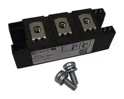
MCMA260P1600YA
THYRISTOR MODULE, 260A, 1.6KV
⚠️ Reference pricing provided. In case of supply shortages, we will connect you with our trusted procurement partners to ensure your project's continuity.
- Manufacturer: IXYS SEMICONDUCTOR
- Product type: Thyristors - SCR Modules
- SVHC: No SVHC (12-Jan-2017)
- No. of Pins: 7Pins
- Product Range: -
- SCR Module Type: Series Connected - SCRs
- Thyristor Mounting: Panel
- On State RMS Current: 408A
- Thyristor Case Style: Y4
- Average Forward Current: 260A
- Gate Trigger Current Max: 150mA
- Gate Trigger Voltage Max: 2V
- Operating Temperature Max: 125°C
- Repetitive Peak Reverse Voltage: 1.6kV
- Peak Repetitive Off State Voltage: 1.6kV
| Delivery and price | |
|---|---|
| Units per pack | 10 |
| Price | 71.47 € |
| Current stock | 10+ |
| Lead time | 30 days |
Datasheet

## **MCMA260P1600YA**

## **Thyristor Module**

**VRRM** _**=**_ **2x 1600 V I TAV** _**=**_ **260 A VT** _**=**_ **1.06 V**

## Phase leg

## **Part number**

## **MCMA260P1600YA**

**==> picture [66 x 7] intentionally omitted <==**

**----- Start of picture text -----**<br>
Backside: isolated<br>**----- End of picture text -----**<br>


**==> picture [173 x 18] intentionally omitted <==**

**----- Start of picture text -----**<br>
3 1 2<br>6 7 5 4<br>**----- End of picture text -----**<br>


## **Features / Advantages:**

- Thyristor for line frequency

- Planar passivated chip

- Long-term stability

- Direct Copper Bonded Al2O3-ceramic

## **Applications:**

- Line rectifying 50/60 Hz

- Softstart AC motor control

- DC Motor control

- Power converter

- AC power control

- Lighting and temperature control

## Y4

## **Package:**

- Isolation Voltage:          V~4800

- Industry standard outline

- RoHS compliant

- Soldering pins for PCB mounting

- Base plate: DCB ceramic

- Reduced weight

- Advanced power cycling

## **Disclaimer Notice**

Information furnished is believed to be accurate and reliable. However, users should independently evaluate the suitability of and test each product selected for their own applications. Littelfuse products are not designed for, and may not be used in, all applications. Read complete Disclaimer Notice at www.littelfuse.com/disclaimer-electronics.

IXYS reserves the right to change limits, conditions and dimensions.

Data according to IEC 60747and per semiconductor unless otherwise specified

20190618d

© 2019 IXYS all rights reserved

**MCMA260P1600YA**

|**Thyristor**|**Thyristor**|**Ratings**|**Ratings**|**Ratings**|**Ratings**|**Ratings**|
|---|---|---|---|---|---|---|
|**Symbol**<br>**Definition**<br>**Conditions**|||**min.**|**typ.**|**max.**|**Unit**|
|**V**<br>**RSM/DSM**<br>_max. non-repetitive reverse/forward blocking voltage_||T    =   25°C<br>VJ|||1700|V|
|**V**<br>**RRM/DRM**<br>_max. repetitive reverse/forward blocking voltage_||T    =   25°C<br>VJ|||1600|V|
|**I**<br>**R/D**<br>_reverse current, drain current_|V    =          V<br>V    =          V<br>1600<br>1600<br>R/D<br>R/D|T    =   25°C<br>VJ<br>T    =       °C<br>VJ<br>140|||300<br>20|mA<br>µA|
|**VT**<br>_forward voltage drop_|I   =         A<br>T<br>200<br>I   =         A<br>400<br>T|T    =   25°C<br>VJ|||1.12<br>1.33|V<br>V|
||I   =         A<br>T<br>200<br>I   =         A<br>400<br>T|T    =       °C<br>VJ<br>125|||1.06<br>1.31|V<br>V|
|**I**<br>**I**<br>_RMS forward current_<br>**T(RMS)**<br>**TAV**<br>_average forward current_|T  =       °C<br>C<br>85<br>180° sine|T    =       °C<br>VJ<br>140|||260<br>408|A<br>A|
|**VT0**<br>**rT**<br>_threshold voltage_<br>_slope resistance_<br>_for power loss calculation only_||T    =       °C<br>VJ<br>140|||0.81<br>1.23|V<br>mΩ|
|**R**<br>**thJC**<br>_thermal resistance junction to case_|||||0.13|K/W|
|**RthCH**<br>_thermal resistance case to heatsink_||||0.07||K/W|
|**Ptot**<br>_total power dissipation_||T    =   25°C<br>C|||880|W|
|**ITSM**<br>_max. forward surge current_|t =  10 ms; (50 Hz), sine<br>t = 8,3 ms; (60 Hz), sine|T    =   45°C<br>VJ<br>V    = 0 V<br>R|||8.30<br>8.97|kA<br>kA|
||t =  10 ms; (50 Hz), sine|T    =       °C<br>VJ<br>140|||7.06<br>7.62|kA<br>kA|
||<br>t = 8,3 ms; (60 Hz), sine|V    = 0 V<br>R|||||
|**I²t**<br>_value for fusing_|t =  10 ms; (50 Hz), sine<br>t = 8,3 ms; (60 Hz), sine|T    =   45°C<br>V    = 0 V<br>VJ<br>R|||344.5<br>334.3|kA²s<br>kA²s|
||t =  10 ms; (50 Hz), sine<br>t = 8,3 ms; (60 Hz), sine|T    =       °C<br>140<br>V    = 0 V<br>VJ<br>R|||248.9<br>241.6|kA²s<br>kA²s|
|**CJ**<br>_junction capacitance_|V  =         V<br>400<br>f = 1 MHz<br>R|T    =   25°C<br>VJ||366||pF|
|**PGM**<br>_max. gate power dissipation_<br>**PGAV**<br>_average gate power dissipation_|t  =   30 µs<br>P<br>t  =<br>P<br>500 µs|T    =       °C<br>C<br>140|||120<br>60<br>20|W<br>W<br>W|
|**(di/dt)cr**<br>_critical rate of rise of current_|repetitive,   I   =<br>TVJ = 140°C; f = 50 Hz<br>t  =        µs;<br>I<br>A; V  =⅔V<br>780 A<br>T<br>P<br>G =<br>0.5<br>di  /dt<br>A/µs;<br>G<br>= 0.5<br>DRM<br>non-repet., I   = 260 A<br>T<br>200|repetitive,   I   =<br>780 A<br>T|||100|A/µs|
||||||500|A/µs|
|**(dv/dt)**<br>_critical rate of rise of voltage_<br>**cr**|T<br>= 140°C<br>R     =∞; method 1 (linear voltage rise)<br>VJ<br>V  =⅔VDRM<br>GK||||1000|V/µs|
|**VGT**<br>_gate trigger voltage_<br>**IGT**<br>_gate trigger current_|V = 6 V<br>T<br>=<br>°C<br>25<br>D<br>VJ<br>T<br>=<br>°C<br>-40<br>VJ<br>V = 6 V<br>T<br>=<br>°C<br>25<br>D<br>VJ<br>T<br>=<br>°C<br>-40<br>VJ||||2<br>150<br>3<br>220|V<br>mA<br>V<br>mA|
|**VGD**<br>_gate non-trigger voltage_<br>**IGD**<br>_gate non-trigger current_|T<br>=<br>°C<br>VJ<br>V  =⅔V<br>D<br>DRM<br>140||||0.25<br>10|V<br>mA|
|_latching current_<br>**IL**|T<br>=<br>°C<br>VJ<br>25<br>t<br>µs<br>p =<br>30<br>I<br>A;<br>=<br>05<br>di  /dt<br>A/s<br><br>=<br>05||||200|mA|
||G <br>.<br> <br>µ<br>G<br><br>.||||||
|_holding current_<br>**IH**|T<br>=<br>°C<br>VJ<br>25<br>V = 6 V<br>D<br>R    =∞<br>GK||||150|mA|
|_gate controlled delay time_<br>**tgd**|T<br>=<br>°C<br>VJ<br>25<br>I<br>A;<br>G =<br>0.5<br>di  /dt<br>A/µs<br>G<br>=<br>0.5<br>V   = ½ V<br>D<br>DRM||||2|µs|
|_turn-off time_<br>**tq**|T<br>=<br>°C<br>VJ<br>di/dt =<br>A/µs<br>10<br>dv/dt =<br>V/µs<br>50<br>V   =<br>R<br>100 V; I<br>A;<br>T = 260<br>V  =⅔VDRM<br>t<br>µs<br>p = 200<br>125|||200||µs|


IXYS reserves the right to change limits, conditions and dimensions.

Data according to IEC 60747and per semiconductor unless otherwise specified

20190618d

© 2019 IXYS all rights reserved

**MCMA260P1600YA**

|**Symbol**<br>**Definition**<br>**Conditions**|**Symbol**<br>**Definition**<br>**Conditions**|**min.**|**typ.**|**max.**|**Unit**|
|---|---|---|---|---|---|
|**I RMS**<br>_RMS current_<br>per terminal<br>~~TT~~||~~TT~~|~~TT~~|300|A|
|**TVJ**<br>_virtual junction temperature_<br>~~TT~~||-40<br>~~TT~~|~~TT~~|140|°C|
|**Top**<br>_operation temperature_||-40||125|°C|
|**Tstg**<br>_storage temperature_||-40||125|°C|
|**Weight**|||150||g|
|**M D**<br>_mounting torque_<br>**M T**<br>_terminal torque_<br>~~|~~||2.25<br>4.5<br>~~|~~|~~|~~|2.75<br>5.5|Nm<br>Nm|
|**dSpp/App**<br>_creepage distance on surface | striking distance through air_<br>**dSpb/Apb**<br>_terminal to backside_<br>_terminal to terminal_|14.0<br>16.0<br>~~|~~|10.0<br>16.0<br>~~|~~|~~|~~||mm<br>mm|
|**V**<br>t = 1 second<br>t = 1 minute<br>_isolation voltage_<br>50/60 Hz, RMS; I≤1 mA<br>ISOL<br>**ISOL**||4800<br>4000|||V<br>V|


**==> picture [185 x 52] intentionally omitted <==**

**----- Start of picture text -----**<br>
Date Code (DC) Circuit<br> + yywwAA<br>Production Part Number<br>Index (PI) Lot.No: xxxxxx<br>Data Matrix:  part no.  (1-19), DC +  PI  (20-25),  lot.no.#  (26-31),<br>blank  (32),  serial no.#  (33-36)<br>**----- End of picture text -----**<br>


|**Part description**|**Part description**|**Part description**|
|---|---|---|
|M|=|Module|
|C|=|Thyristor (SCR)|
|M|=|Thyristor|
|A|=|(up to 1800V)|
|260|=|Current Rating [A]|
|P|=|Phase leg|
|1600|=|Reverse Voltage [V]|
|YA|=|Y4-M6|


**Ordering Ordering Number Marking on Product Delivery Mode Quantity Code No.** ~~se~~ Standard MCMA260P1600YA MCMA260P1600YA Box 6 509785

|**Equivalent Circuits for Simulation**|**Equivalent Circuits for Simulation**|**Equivalent Circuits for Simulation**|**Equivalent Circuits for Simulation**|_* on die level_|T    =<br>VJ|140 °C|
|---|---|---|---|---|---|---|
|**V0 max**<br>I<br>V0<br>~~~~~|_threshold voltage_<br>~~R~~0|_threshold voltage_|0.81<br>**Thyristor**|||V|
|**R0 max**|_slope resistance *_||0.59|||mΩ|


IXYS reserves the right to change limits, conditions and dimensions.

Data according to IEC 60747and per semiconductor unless otherwise specified

20190618d

© 2019 IXYS all rights reserved

**MCMA260P1600YA**

## **Outlines Y4**

**==> picture [509 x 483] intentionally omitted <==**

**----- Start of picture text -----**<br>
M6 2.8/0.8 MIN MAX MIN MAX<br>Dim.<br>a p [mm] [mm] [inch] [inch]<br>a 30.0 30.6 1.181 1.205<br>b typ. 0.25 typ. 0.010<br>c 64.0 65.0 2.520 2.559<br>d 6.5 7.0 0.256 0.275<br>e 4.9 5.1 0.193 0.201<br>c f f 28.6 29.2 1.126 1.150<br>A g 7.3 7.7 0.287 0.303<br>h<br>h 93.5 94.5 3.681 3.720<br>i q k i 79.5 80.5 3.130 3.169<br>j 4.8 5.2 0.189 0.205<br>1 2 3 C C k 33.4 34.0 1.315 1.339<br>o<br>l 16.7 17.3 0.657 0.681<br>m 22.7 23.3 0.894 0.917<br>B n 22.7 23.3 0.894 0.917<br>o 14.0 15.0 0.551 0.591<br>B p typ. 10.5 typ. 0.413<br>n m l<br>q 22.8 23.3 0.898 0.917<br>Optional accessories for modules r 1.8 2.4 0.071 0.041<br>Keyed gate/cathode twin plugs with wire length = 350 mm, gate = white, cathode = red<br>Type ZY 180L  (L = Left for pin pair 4/5)<br>UL 758, style 3751<br>Type ZY 180R (R = Right for pin pair 6/7)<br>A (3:1) B-B (1:1) j r C-C (1:1) g<br>b<br>DCB e<br>nd<br>11<br>8 9<br>10 6 7<br>5 4<br>**----- End of picture text -----**<br>


**==> picture [509 x 168] intentionally omitted <==**

**----- Start of picture text -----**<br>
3 1 2<br>6 7 5 4<br>**----- End of picture text -----**<br>


IXYS reserves the right to change limits, conditions and dimensions.

Data according to IEC 60747and per semiconductor unless otherwise specified

20190618d

© 2019 IXYS all rights reserved

**MCMA260P1600YA**

**==> picture [509 x 681] intentionally omitted <==**

**----- Start of picture text -----**<br>
Thyristor<br>400 7000 10 [6]<br>50 Hz, 80% VRRM V R  = 0 V<br>300 6000<br>IT ITSM TVJ = 45°C I [2] t T VJ  = 45°C TVJ = 140°C<br>200 5000 10 [5]<br>[A] [A]<br>[A [2] s]<br>TVJ = 125°C<br>100 140°C 4000 TVJ = 140°C<br>TVJ = 25°C<br>0 3000 10 [4]<br>0.0 0.5 1.0 1.5 0.01 0.1 1 1 2 3 4 5 6 7 8 910<br>VT [V] t [s] t [ms]<br>Fig. 1  Forward current vs. Fig. 2 Surge overload current Fig. 3 I [2] t vs. time per thyristor<br>voltage drop per thyristor vs. time per thyristor<br>10 1: I GT , T VJ = 125°C 100.0 320 dc =<br>2: IGT, TVJ = 25 ° C 1<br>3: IGT, TVJ = -40°C 0.5<br>0.4<br>240<br>3 TVJ = 125°C 0.33<br>10.0 0.17<br>2 6<br>VG 1 4 5 tgd ITAVM 0.08<br>1 160<br>[V] [µs] lim. [A]<br>1.0<br>typ.<br>80<br>4: P GM = 20 W<br>IGD, TVJ = 140°C 5: PGM = 60 W<br>0.1 6: P GM = 120 W 0.1 0<br>10 [-3] 10 [-2] 10 [-1] 10 [0] 10 [1] 10 [2] 0.01 0.10 1.00 10.00 0 40 80 120 160<br>IG [A] IG [A] Tcase [°C]<br>Fig. 4 Gate voltage & gate current Fig. 5 Gate controlled delay time tgd Fig. 6 Max. forward current vs.<br>case temperature per thyr.<br>420 0.16<br>RthHA i Rthi  (K/W) ti  (s)<br>350 dc = 1 0.20.4 12 0.01000.0065 0.000140.01900<br>0.6 0.12<br>0.5 3 0.0250 0.18000<br>0.8<br>280 0.4 4 0.0615 0.52000<br>1.0<br>Ptot 0.330.17 2.0 ZthJC 5 0.0270 1.60000<br>210 0.08 0.08<br>[W] [K/W]<br>140<br>0.04<br>70<br>0 0.00<br>0 80 160 240 320 0 70 140 1 10 100 1000 10000<br>IT(AV) [A] Tamb [°C] t   [ms]<br>Fig. 8  Transient thermal impedance junction to case<br>Fig. 7 Power dissipation vs. forward current<br>vs. time per thyristor<br>and ambient temperature per thyristor<br>**----- End of picture text -----**<br>


IXYS reserves the right to change limits, conditions and dimensions.

Data according to IEC 60747and per semiconductor unless otherwise specified

20190618d

© 2019 IXYS all rights reserved
Updated at June 7, 2026
About Novapart
Novapart is a B2B electronic component broker specialising in stock shortages and cost reduction. We source hard-to-find parts and identify compliant alternatives across a catalogue of 410,000+ components from 500+ manufacturers.
Learn more →Stock Shortage Specialist
When a component is unavailable, discontinued or has an unacceptable lead time, we tap into our network of vetted European and Asian distributors to source what you need — without compromising on quality or traceability.
Request a quote →Compliant Alternatives
We identify pin-to-pin, electrically equivalent substitutes that meet the same certifications (RoHS, AEC-Q100, REACH) as your original specification — validated against datasheets, not just part numbers. Often at a lower cost.
BOM Analysis service →