
Image not available
Illustrative purposes only

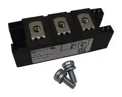
MCC162-16IO1
Thyristor Module, 181A, 1.6kV
⚠️ Reference pricing provided. In case of supply shortages, we will connect you with our trusted procurement partners to ensure your project's continuity.
- Manufacturer: IXYS SEMICONDUCTOR
- Product type: Thyristors - SCR Modules
- SCR Module Type:Series Connected - SCRs; Peak Repetitive Off-State Voltage, Vdrm:1.6kV; Gate Trigger Current Max, Igt:150mA; Current It av:181A; On State RMS Current IT(rms):300A; Peak Non
- SVHC: No SVHC (17-Jan-2023)
- No. of Pins: 7Pins
- Product Range: -
- SCR Module Type: Series Connected - SCRs
- Thyristor Mounting: Panel
- On State RMS Current: 300A
- Thyristor Case Style: Y4
- Average Forward Current: 181A
- Gate Trigger Current Max: 150mA
- Gate Trigger Voltage Max: 2.5V
- Operating Temperature Max: 100°C
- Repetitive Peak Reverse Voltage: 1.6kV
- Peak Repetitive Off State Voltage: 1.6kV
| Delivery and price | |
|---|---|
| Units per pack | 10 |
| Price | 40.95 € |
| Current stock | 10+ |
| Lead time | 30 days |
Datasheet

## **MCC162-16io1**

## **Thyristor Module**

VRRM = 2x 1600 V I TAV = 181 A VT = 1.03 V

## Phase leg

## **Part number**

MCC162-16io1

**==> picture [66 x 7] intentionally omitted <==**

**----- Start of picture text -----**<br>
Backside: isolated<br>**----- End of picture text -----**<br>


**==> picture [173 x 18] intentionally omitted <==**

**----- Start of picture text -----**<br>
3 1 2<br>6 7 5 4<br>**----- End of picture text -----**<br>


## **Features / Advantages:**

- Thyristor for line frequency

- Planar passivated chip

- Long-term stability

- Direct Copper Bonded Al2O3-ceramic

## **Applications:**

- Line rectifying 50/60 Hz

- Softstart AC motor control

- DC Motor control

- Power converter

- AC power control

- Lighting and temperature control

## Y4

## **Package:**

- Isolation Voltage:          V~3600

- Industry standard outline

- RoHS compliant

- Soldering pins for PCB mounting

- Base plate: DCB ceramic

- Reduced weight

- Advanced power cycling

IXYS reserves the right to change limits, conditions and dimensions.

Data according to IEC 60747and per semiconductor unless otherwise specified

20131121a

© 2013 IXYS all rights reserved

**MCC162-16io1**

|**Thyristor**|**Thyristor**|Ratings|Ratings|Ratings|Ratings|Ratings|
|---|---|---|---|---|---|---|
|Symbol<br>Definition<br>Conditions|||min.|typ.|max.|Unit|
|V<br>RSM/DSM<br>_max. non-repetitive reverse/forward blocking voltage_||T    =   25°C<br>VJ|||1700|V|
|V<br>RRM/DRM<br>_max. repetitive reverse/forward blocking voltage_||T    =   25°C<br>VJ|||1600|V|
|I<br>R/D<br>_reverse current, drain current_|V    =          V<br>V    =          V<br>1600<br>1600<br>R/D<br>R/D|T    =   25°C<br>VJ<br>T    =       °C<br>VJ<br>125|||300<br>10|mA<br>µA|
|V T<br>_forward voltage drop_|I   =         A<br>T<br>150<br>I   =         A<br>300<br>T|T    =   25°C<br>VJ|||1.09<br>1.25|V<br>V|
||I   =         A<br>T<br>150<br>I   =         A<br>300<br>T|T    =       °C<br>VJ<br>125|||1.03<br>1.25|V<br>V|
|I<br>I<br>_RMS forward current_<br>T(RMS)<br>TAV<br>_average forward current_|T  =       °C<br>C<br>85<br>180° sine|T    =       °C<br>VJ<br>125|||181<br>300|A<br>A|
|VT0<br>r T<br>_threshold voltage_<br>_slope resistance_<br>_for power loss calculation only_||T    =       °C<br>VJ<br>125|||0.88<br>1.15|V<br>mΩ|
|R<br>thJC<br>_thermal resistance junction to case_|||||0.155|K/W|
|RthCH<br>_thermal resistance case to heatsink_||||0.07||K/W|
|Ptot<br>_total power dissipation_||T    =   25°C<br>C|||645|W|
|ITSM<br>_max. forward surge current_|t =  10 ms; (50 Hz), sine<br>t = 8,3 ms; (60 Hz), sine|T    =   45°C<br>VJ<br>V    = 0 V<br>R|||6.00<br>6.48|kA<br>kA|
||t =  10 ms; (50 Hz), sine|T    =       °C<br>VJ<br>125|||5.10<br>5.51|kA<br>kA|
||<br>t = 8,3 ms; (60 Hz), sine|V    = 0 V<br>R|||||
|I²t<br>_value for fusing_|t =  10 ms; (50 Hz), sine<br>t = 8,3 ms; (60 Hz), sine|T    =   45°C<br>V    = 0 V<br>VJ<br>R|||180.0<br>174.7|kA²s<br>kA²s|
||t =  10 ms; (50 Hz), sine<br>t = 8,3 ms; (60 Hz), sine|T    =       °C<br>125<br>V    = 0 V<br>VJ<br>R|||130.1<br>126.3|kA²s<br>kA²s|
|CJ<br>_junction capacitance_|V  =         V<br>400<br>f = 1 MHz<br>R|T    =   25°C<br>VJ||273||pF|
|PGM<br>_max. gate power dissipation_<br>PGAV<br>_average gate power dissipation_|t  =   30 µs<br>P<br>t  =<br>P<br>500 µs|T    =       °C<br>C<br>125|||120<br>60<br>8|W<br>W<br>W|
|(di/dt)cr<br>_critical rate of rise of current_|TVJ = 125°C; f = 50 Hz<br>t  =        µs;<br>I<br>A; V  = ⅔ V<br>P<br>G =<br>0.5<br>di  /dt<br>A/µs;<br>G<br>=<br>0.5<br>D<br>DRM<br>200|repetitive,   I   =<br>540 A<br>T|||150|A/µs|
|||non-repet., I   = 180 A<br>T|||500|A/µs|
|(dv/dt)<br>_critical rate of rise of voltage_<br>cr|T<br>= 125°C<br>R     = ∞; method 1 (linear voltage rise)<br>VJ<br>V  =  ⅔ V<br>D<br>DRM<br>GK||||1000|V/µs|
|VGT<br>_gate trigger voltage_<br>IGT<br>_gate trigger current_|V = 6 V<br>T<br>=<br>°C<br>25<br>D<br>VJ<br>T<br>=<br>°C<br>-40<br>VJ<br>V = 6 V<br>T<br>=<br>°C<br>25<br>D<br>VJ<br>T<br>=<br>°C<br>-40<br>VJ||||2.5<br>150<br>2.6<br>200|V<br>mA<br>V<br>mA|
|VGD<br>_gate non-trigger voltage_<br>IGD<br>_gate non-trigger current_|T<br>=<br>°C<br>VJ<br>V  =  ⅔ V<br>D<br>DRM<br>125||||0.2<br>10|V<br>mA|
|_latching current_<br>IL|T<br>=<br>°C<br>VJ<br>25<br>t<br>µs<br>p =<br>30<br>I<br>A;<br>=<br>05<br>di  /dt<br>A/µs<br><br>=<br>05||||300|mA|
||G <br>.<br> <br><br>G<br>.||||||
|_holding current_<br>IH|T<br>=<br>°C<br>VJ<br>25<br>V = 6 V<br>D<br>R    = ∞<br>GK||||200|mA|
|_gate controlled delay time_<br>t gd|T<br>=<br>°C<br>VJ<br>25<br>I<br>A;<br>G =<br>0.5<br>di  /dt<br>A/µs<br>G<br>=<br>0.5<br>V   = ½ V<br>D<br>DRM||||2|µs|
|_turn-off time_<br>t q|T<br>=<br>°C<br>VJ<br>di/dt =<br>A/µs;<br>10<br>dv/dt =<br>V/µs;<br>20<br>V   =<br>R<br>100 V; I<br>A;<br>T = 300<br>V  =  ⅔ V<br>D<br>DRM<br>t<br>µs<br>p = 200<br>125|||150||µs|
||||||||


IXYS reserves the right to change limits, conditions and dimensions.

Data according to IEC 60747and per semiconductor unless otherwise specified

20131121a

© 2013 IXYS all rights reserved

**MCC162-16io1**

|Symbol<br>Definition<br>Conditions|Symbol<br>Definition<br>Conditions|min.|typ.|max.|Unit|
|---|---|---|---|---|---|
|I RMS<br>_RMS current_<br>per terminal||||300|A|
|TVJ<br>_virtual junction temperature_||-40||125|°C|
|Top<br>_operation temperature_||-40||100|°C|
|Tstg<br>_storage temperature_||-40||125|°C|
|Weight|||150||g|
|M D<br>_mounting torque_<br>M T<br>_terminal torque_||2.25<br>4.5<br>~~aa~~|~~aa~~|2.75<br>5.5|Nm<br>Nm|
|d Spp/App<br>_creepage distance on surface | striking distance through air_<br>d Spb/Apb<br>_terminal to backside_<br>_terminal to terminal_|14.0<br>16.0|10.0<br>16.0<br>~~aa~~|~~aa~~||mm<br>mm|
|V<br>t = 1 second<br>t = 1 minute<br>_isolation voltage_<br>50/60 Hz, RMS; I      ≤ 1 mA<br>ISOL<br>ISOL||3600<br>3000|||V<br>V|


**==> picture [181 x 29] intentionally omitted <==**

**----- Start of picture text -----**<br>
AssemblyLine Circuit Diagram<br>Date Code yywwA<br>Part No. YYYYYYYYYYY og 2D Matrix<br>**----- End of picture text -----**<br>


|Ordering|Part Number|Markingon Product|DeliveryMode|Quantity|Code No.|
|---|---|---|---|---|---|
|Standard|MCC162-16io1|MCC162-16io1|Box|6|429619|


|**Equivalent Circuits for Simulation**<br>T    =<br>VJ<br>125 °C<br>_* on die level_<br>~~a~~|**Equivalent Circuits for Simulation**<br>T    =<br>VJ<br>125 °C<br>_* on die level_<br>~~a~~|**Equivalent Circuits for Simulation**<br>T    =<br>VJ<br>125 °C<br>_* on die level_<br>~~a~~|
|---|---|---|
|I<br>V0<br>~~R~~0||Thyristor|
||||
|_threshold voltage_<br>V 0 max||V<br>0.88|
|R0 max<br>_slope resistance *_||mΩ<br>0.8|


IXYS reserves the right to change limits, conditions and dimensions.

Data according to IEC 60747and per semiconductor unless otherwise specified

20131121a

© 2013 IXYS all rights reserved

**MCC162-16io1**

## **Outlines Y4**

**==> picture [371 x 420] intentionally omitted <==**

**----- Start of picture text -----**<br>
M6 x 16 2.8 / 0.8<br>1 2 3<br>65<br>Ø 6.6<br>94<br>80 7<br>5<br>6<br>7<br>11 10 1 2 3<br>8 9<br>17 4<br>5<br>40<br>63<br>2.2<br>30 29<br>5<br>0.25<br>15 34<br>12.4 23.2<br>**----- End of picture text -----**<br>


## Optional accessories for modules

Keyed gate/cathode twin plugs with wire length = 350 mm, gate = white, cathode = red Type ZY 180L  (L = Left for pin pair 4/5) UL 758, style 3751 Type ZY 180R (R = Right for pin pair 6/7)

**==> picture [483 x 168] intentionally omitted <==**

**----- Start of picture text -----**<br>
3 1 2<br>6 7 5 4<br>**----- End of picture text -----**<br>


IXYS reserves the right to change limits, conditions and dimensions.

Data according to IEC 60747and per semiconductor unless otherwise specified

20131121a

© 2013 IXYS all rights reserved

**MCC162-16io1**

## **Thyristor**

**==> picture [317 x 406] intentionally omitted <==**

**----- Start of picture text -----**<br>
5000 10 [6]<br>50 Hz<br>4000 80% V RRM<br>ITSM TVJ = 45°C<br>TVJ = 125°C<br>3000 I [2] dt<br>[A] 10 [5] TVJ = 45°C<br>2000 [A [2] s] T VJ  = 125°C<br>1000<br>0 10 [4]<br>0.001 0.01 0.1 1 1 10<br>t [s] t [ms]<br>Fig. 1 Surge overload current ITSM,TSM,, Fig. 2 I [[2]] t versus time (1-10 ms)<br>IFSM: Crest value, t: durationFSM: Crest value, t: duration: Crest value, t: duration<br>400<br>360 RthKA K/W<br>0.3<br>320 0.4<br>0.5<br>280 0.6<br>0.8<br>Ptot 240 1.01.4<br>200 1.8<br>[W] 160 DC180° sin<br>120°<br>120  60°<br> 30°<br>80<br>40<br>0<br>0 50 100 150 200 250 0 25 50 75 100 125 150<br>ITAVM [A] Ta [°C]<br>**----- End of picture text -----**<br>


**==> picture [289 x 25] intentionally omitted <==**

**----- Start of picture text -----**<br>
Fig. 1 Surge overload current ITSM,TSM,, Fig. 2 I [[2]] t versus time (1-10 ms)<br>IFSM: Crest value, t: durationFSM: Crest value, t: duration: Crest value, t: duration<br>**----- End of picture text -----**<br>


**==> picture [264 x 19] intentionally omitted <==**

**----- Start of picture text -----**<br>
Fig. 4 Power dissipation vs. on-state current & ambient temperature<br>(per thyristor or diode)<br>**----- End of picture text -----**<br>


**==> picture [309 x 176] intentionally omitted <==**

**----- Start of picture text -----**<br>
1400 RthKA K/W<br>0.03<br>1200 0.04<br>Circuit 0.06<br>B6 0.08<br>1000 3xMCC162 or 0.1<br>Ptot 3x MCD162 0.15<br>800 0.2<br>0.3<br>[W]<br>600<br>400<br>200<br>0<br>0 100 200 300 400 500 0 25 50 75 100 125 150<br>IdAVM [A] T a  [°C]<br>**----- End of picture text -----**<br>


**==> picture [258 x 19] intentionally omitted <==**

**----- Start of picture text -----**<br>
Fig. 6 Three phase rectifier bridge: Power dissipation versus direct<br>output current and ambient temperature<br>**----- End of picture text -----**<br>


**==> picture [155 x 178] intentionally omitted <==**

**----- Start of picture text -----**<br>
320<br>280 DC<br>180° sin<br>120°<br>240  60°<br> 30°<br>200<br>ITAVM<br>160<br>[A]<br>120<br>80<br>40<br>0<br>0 25 50 75 100 125 150<br>TC [°C]<br>**----- End of picture text -----**<br>


Fig. 3 Max. forward current at case temperature

**==> picture [139 x 180] intentionally omitted <==**

**----- Start of picture text -----**<br>
100<br>tp = 30 µs<br>tp = 500 µs<br>P GM = 120 W<br>60 W<br>10 PGAV = 8 W<br>VG<br>[V]<br>1<br>IGT (TVJ = -40°C)<br>IGT (TVJ = 0°C)<br>I GT (T VJ = 25°C)<br>0.1 IGD<br>0.01 0.1 1 10<br>IG [A]<br>125°C 25°C<br>**----- End of picture text -----**<br>


Fig. 5 Gate trigger characteristics

**==> picture [147 x 195] intentionally omitted <==**

**----- Start of picture text -----**<br>
100<br>T VJ = 25°C<br>10<br>t<br>gd<br>[μs] limit<br>1<br>typ.<br>0.1<br>0.01 0.1 1 10<br>IG [A]<br>Fig. 7 Gate trigger delay time<br>**----- End of picture text -----**<br>


IXYS reserves the right to change limits, conditions and dimensions.

Data according to IEC 60747and per semiconductor unless otherwise specified

20131121a

© 2013 IXYS all rights reserved

**MCC162-16io1**

## **Thyristor**

**==> picture [324 x 417] intentionally omitted <==**

**----- Start of picture text -----**<br>
1600<br>RthKA K/W<br>Circuit<br>W3 0.03<br>3xMCC162 or 0.04<br>1200 3xMCD162 0.06<br>0.08<br>0.1<br>0.15<br>Ptot 800 0.2<br>0.3<br>[W]<br>400<br>0<br>0 100 200 300 400 0 25 50 75 100 125 150<br>IRMS [A] Ta [°C]<br>Fig. 8 Three phase AC-controller: Power dissipation versus<br>RMS output current and ambient temperature<br>0.24<br>0.16<br>ZthJC 30°<br>60°<br>[K/W] 120°180°<br>0.08 DC<br>0.00<br>10 [-3] 10 [-2] 10 [-1] 10 [0] 10 [1] 10 [2]<br>t [s]<br>Fig. 9 Transient thermal impedance junction to case (per thyristor/diode)<br>**----- End of picture text -----**<br>


**==> picture [113 x 69] intentionally omitted <==**

**----- Start of picture text -----**<br>
RthJC for various conduction angles d:<br>d   RthJC [K/W]<br> DC   0.155<br>180° 0.167<br>120° 0.176<br>60° 0.197<br>30° 0.227<br>**----- End of picture text -----**<br>


Constants for ZthJC calculation: i Rthi [K/W] ti [s] 1 0.0072 0.001 2 0.0188 0.080 3 0.1290 0.200

**==> picture [502 x 185] intentionally omitted <==**

**----- Start of picture text -----**<br>
0.3<br>RthJK for various conduction angles d:<br>d   RthJK [K/W]<br> DC   0.225<br>180° 0.237<br>0.2<br>120° 0.246<br>30° 60° 0.267<br>ZthJK 120°60° 30° 0.297<br>180°<br>[K/W] 0.1 DC Constants for ZthJK calculation:<br>i  Rthi [K/W]   ti [s]<br>1 0.0072  0.001<br>2 0.0188  0.080<br>3 0.1290  0.200<br>0.0 4 0.0700  1.000<br>10 [-3] 10 [-2] 10 [-1] 10 [0] 10 [1] 10 [2]<br>t [s]<br>Fig. 10 Transient thermal impedance junction to heatsink (per thyristor/diode)<br>**----- End of picture text -----**<br>


IXYS reserves the right to change limits, conditions and dimensions.

Data according to IEC 60747and per semiconductor unless otherwise specified

20131121a

© 2013 IXYS all rights reserved
Updated at June 7, 2026
About Novapart
Novapart is a B2B electronic component broker specialising in stock shortages and cost reduction. We source hard-to-find parts and identify compliant alternatives across a catalogue of 410,000+ components from 500+ manufacturers.
Learn more →Stock Shortage Specialist
When a component is unavailable, discontinued or has an unacceptable lead time, we tap into our network of vetted European and Asian distributors to source what you need — without compromising on quality or traceability.
Request a quote →Compliant Alternatives
We identify pin-to-pin, electrically equivalent substitutes that meet the same certifications (RoHS, AEC-Q100, REACH) as your original specification — validated against datasheets, not just part numbers. Often at a lower cost.
BOM Analysis service →