
Image not available
Illustrative purposes only

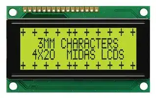
MC42005B6W-SPR
Alphanumeric LCD, 20 x 4, Black on Yellow / Green, 5V, Parallel, English, Japanese, Reflective
⚠️ Reference pricing provided. In case of supply shortages, we will connect you with our trusted procurement partners to ensure your project's continuity.
- Manufacturer: MIDAS
- Product type: Alphanumeric LCD Displays
- Font Set: English, Japanese
- Module Size: 98mm x 60mm
- Display Mode: Reflective
- Logic Voltage: 5V
- Product Range: MC42005B6W
- Character Size: 4.75mm
- Interface Type: Parallel
- LCD Display Type: STN
- Display Appearance: Black on Yellow / Green
- Backlighting Colour: No Backlight
- Display Construction: COB
- Character Count x Line: 20 x 4
- Operating Temperature Max: 70°C
- Operating Temperature Min: -20°C
| Delivery and price | |
|---|---|
| Units per pack | 250 |
| Price | 8.4 € |
| Current stock | 10+ |
| Lead time | 30 days |
Datasheet

**Midas Components Limited Telephone** +44 (0)1493 602602 Electra House **Fax** +44 (0)1493 665111 32 Southtown Road **Email** sales@midasdisplays.com Great Yarmouth **Website** www.midasdisplays.com Norfolk NR31 0DU England

## **S ecification p**

Part Number: Version: ~~a~~ Date:

**Revision No. Date Description Item Page**

BOOKBINDING AREA

## DOC.

## DATASHEET STATEMENT

**1.** The following icons are absolutely designed by Midas independently in 2007-SEP. They are not in common use in the LCD industry yet but just used for marking out Midas products’ characteristics quickly and simply without any special meaning. Midas reserves the composing right and copyright. No one else is allowed to adopt these icons without Midas approval.

**2.** The ISO9001 logo used in this document is authorized by SGS (www.sgs.com). Midas had already successfully passed the strict and professional ISO9001:2000 Quality Management System Certification and got the certificate (No.: CN07/00404)

**3.** The technologies/techniques/crafts which denoted by the following icons are not exclusively owned by Midas, but also shared by Midas LCD strategic cooperators, however all these technologies/techniques/crafts have been finally confirmed by Midas professional engineers and QC department.

**4.** As the difference in test standard and test conditions, also Midas insufficient familiarity with the actual LCD using environment, all the referred information in this DATASHEET (including the icons) only have two functions: 4.1: providing quick reference when you are judging whether or not the product meets your requirements. 4.2: listing out definitely the tolerance.

SAMPLE APPROVAL document rather than consider this DATASHEET as the standard for judging whether or not the LCD meets your requirements. Once you instruct Midas to a mass-production without definite demand for providing sample before, Midas will disclaim all responsibility if the mass-production is proved not meeting with your requirements.

**5.** The sequence of the icons is random and doesn’t indicate the importance grade.

**6.** Icons explanation

Midas 2006 version logo.Midas  is an integrated manufacturer of flat panel display (FPD). Midas supplies TN, HTN, STN, FSTN monochrome

LCD panel; COB, COG, TAB LCD module; and all kinds of LED backlight.

**FAST RESPONSE TIME** This icon on the cover indicates the product FFF is with high response speed; Otherwise not. 0 **HIGH CONTRAST** H C This icon on the cover indicates the product is with high contrast; Otherwise not. oF

## **PROTECTION CIRCUIT**

This icon on the cover indicates the product is with protection circuit; Otherwise not.

## **LONG LIFE VERSION**

This icon on the cover indicates the product is long life version (over 9K hours guaranteed); Otherwise not.

## **WIDE VIEWING SCOPE**

This icon on the cover indicates the product is with wide viewing scope; Otherwise not.

## **Anti UV VERSION**

UV This icon on the cover indicates the product is against UV line. Otherwise not.

## RoHS

## **RoHS COMPLIANCE**

This icon on the cover indicates the product meets ROHS requirements; Otherwise not.

## **OPERATION TEMPERATURE RANGE**

Y C

This icon on the cover indicates the operating X C temperature range (X-Y).

## **3TIMEs 100% QC EXAMINATION**

This icon on the cover indicates the product has passed Midas thrice 100% QC. Otherwise not.

## **TWICE SELECTION OF LED MATERIALS**

This icon on the cover indicates the LED had passed Midas twice strict selection which promises the product’s identical color and brightness; Otherwise not.

3.0V

## **Vlcm = 3.0V**

This icon on the cover indicates the product can work at 3.0V exactly; otherwise not.

N ™

## **N SERIES TECHNOLOGY (2008 developed)**

New structure, new craft, new technology and new materials inside both LCD module and LCD panel to improve the "RainBow"

## Contents

1.Module Classification Information

- 2.Precautions in use of LCD Modules

3.General Specification

- 4.Absolute Maximum Ratings

- 5.Electrical Characteristics

6.Optical Characteristics

- 7.Interface Pin Function

8.Power Supply

9.Contour Drawing & Block Diagram

11.Function Description

12.Character Generator ROM Pattern

12.Instruction Table

13.Timing Characteristics

14.Initializing of LCM

15.Quality Assurance

16.Reliability

PAGE  3  OF  22

## **Midas LCD Part Number System**

**==> picture [479 x 28] intentionally omitted <==**

- 1 = **MC:** Midas Components

2

- = **Blank:** COB (chip on board) **COG** : chip on glass

3 = **No of dots** (e.g. 240064 = 240 x 64 dots) (e.g. 21605 = 2 x 16 5mm C.H.)

- 4 = **Series**

- 5 = **Series Variant:** A to Z **– see addendum**

6

7

8

- = **3:** 3 o’clock **6:** 6 o’clock **9** : 9 o’clock **12** : 12 o’clock

- = **S** : Normal (0 to + 50 deg C) **W:** Wide temp. (-20 to + 70 deg C) **X:** Extended temp (-30 + 80 Deg C)

- = **Character Set**

**Blank:** Standard (English/Japanese)

- **C:** Chinese Simplified (Graphic Displays only)

- **CB:** Chinese Big 5 (Graphic Displays only)

- **H:** Hebrew

- **K:** European (std) (English/German/French/Greek)

- **L:** English/Japanese (special)

- **M:** European (English/Scandinavian)

- **R:** Cyrillic

- **W:** European (English/Greek)

- **U:** European (English/Scandinavian/Icelandic)

9

- = **Bezel Height** (where applicable /available)

||Top of Bezel to Top<br>of PCB|LED Connection<br>Common (via pins 1<br>and 2)|Array or<br>Edge Lit|
|---|---|---|---|
|**Blank**|9.5mm / not<br>applicable|via pins 15+ 16-|Array|
|**2**|8.9 mm|Common|Array|
|**3**|7.8 mm|Separate|Array|
|**4**|7.8 mm|Common|Array|
|**5**|9.5 mm|Separate|Array|
|**6**|7 mm|Common|Array|
|**7**|7 mm|Separate|Array|
|**8**|6.4 mm|Common|Edge|
|**9**|6.4 mm|Separate|Edge|
|**A**|5.5 mm|Common|Edge|
|**B**|5.5 mm|Separate|Edge|
|**D**|6.0mm|Separate|Edge|
|**E**|5.0mm|Separate|Edge|
|**F**|4.7mm|Common|Edge|
|**G**|3.7mm|Separate|EL|
|**H**|7 mm|Separate|Edge|


- 10 = **T:** TN **S** : STN **B:** STN Blue **G:** STN Grey **F:** FSTN **F2:** FFSTN **V:** VA (Vertically Aligned)

- 11 = **P:** Positive **N** : Negative

- 12 = **R:** Reflective **M** : Transmissive **T:** Transflective

- 13 = **Backlight: Blank:** Reflective **L:** LED

- 14 = **Backlight Colour: Y:** Yellow-Green **W:** White **B:** Blue **R:** Red **A:** Amber **O:** Orange **G:** Green **RGB:** R.G.B.

15

16

= **Driver Chip: Blank:** Standard **I:** I[2] C **S** : SPI **T:** Toshiba T6963C **A:** Avant SAP1024B **R:** Raio RA6963 = **Voltage Variant** : e.g. **3** = 3v

F/Displays/Midas Brand/Midas LCD Part Number System 16 Oct 2013.doc

## 2. Precautions in use of LCD Modules

(1)Avoid applying excessive shocks to the module or making any alterations or modifications to it.

(2)Don’t make extra holes on the printed circuit board, modify its shape or change the components of LCD module.

- (3)Don’t disassemble the LCM.

- (4)Don’t operate it above the absolute maximum rating.

- (5)Don’t drop, bend or twist LCM.

- (6)Soldering: only to the I/O terminals.

(7)Storage: please storage in anti-static electricity container and clean environment.

## 3. General Specification

|**Item**|**Dimension**|**Unit**|
|---|---|---|
|Number of Characters<br>~~RVAED~~|20characters x 4 Lines<br>~~EDJeeee~~|~~ee~~|
|Module dimension(No Backlight )<br>~~RVAED~~<br>~~Bee 4....44e~~|98.0 x 60.0 x 10.0<br>MAX<br>~~EDJeeee~~<br>~~....44e~~|mm<br>~~ee~~<br>~~....44e~~<br>~~46~~|
|Module dimension(With LED Backlight )<br>~~RV A ED~~<br>~~Bee 4....44e~~|98.0 x 60.0 x 15.0<br>MAX<br>~~ED Jee ee~~<br>~~....44e~~|mm<br>~~ee~~<br>~~....44e~~<br>~~46~~|
|View area<br>~~Bee 4 ....44e~~|76.0 x 25.2<br>~~....44e~~|mm<br>~~....44e~~<br>~~46~~|
|Active area|70.40 x 20.80|mm|
|Dot size|0.55 x 0.55|mm|
|Dot pitch|0.60 x 0.60|mm|
|Character size|2.95 x 4.75|mm|
|Character pitch|3.55 x 5.35|mm|
|LCD type|STN||
|Duty|1/16||
|View direction|6 o’clock or 12 o’clock||
|Backlight Type|Yellow/Green Reflective||


PAGE  5  OF  22

## 4. Absolute Maximum Ratings

|**Item**<br>~~|.~~<br>~~=ofw~~|**Symbol**<br>~~fwoom,~~|**Condition**<br>~~oom,~~<br>~~isl~~|**Min**<br>~~isl~~|**Typ**<br>~~islor~~|**Max**<br>~~or~~|**Unit**|
|---|---|---|---|---|---|---|
|Supply Voltage For Logic<br>~~|.~~<br>~~=o fw~~<br>~~BAW~~|VDD-VSS<br>~~fw oom,~~<br>~~4~~|~~oom,~~<br>~~isl~~<br>~~7~~|4.5<br>~~isl~~<br>~~eee.~~|5.0<br>~~isl or~~<br>~~eee.~~|5.5<br>~~or~~<br>~~eee.~~|V<br>~~Se~~|
|Supply Voltage For LCD<br>~~BAW~~|VDD-V0<br>~~4~~|Ta=25<br>~~7~~|4.5<br>~~eee.~~|5.0<br>~~eee.~~|5.5<br>~~eee.~~|V<br>~~Se~~|
|Input High Volt.<br>~~BAW ~~|VIH<br> ~~4~~|~~7 ~~|0.7 VDD<br> ~~eee.~~|~~eee.~~|VDD<br>~~eee.~~|V<br>~~Se~~|
|Input Low Volt.|VIL||VSS||0.3 VDD|V|
|Supply Current|IDD|VDD=5V|0.7|0.75|1.5|mA|
|Supply Voltage of<br>Yellow-green backlight|VLED|Forward<br>current<br>=180 mA<br>Number of<br>LED die<br>2x18= 36|4.0|4.2|4.4|V|
|Supply Voltage of White<br>backlight|VLED|Forward<br>current<br>=30 mA<br>Number of<br>LED die<br>2|3.8|4.0|4.2|V|
|Supply Voltage of RED<br>backlight|VLED|Forward<br>current<br>=180 mA<br>Number of<br>LED die<br>2x18= 36|3.5|3.9|4.1|V|


## 5. Electrical Characteristics

PAGE  6  OF  22

## 6. Optical Characteristics

**==> picture [449 x 607] intentionally omitted <==**

**----- Start of picture text -----**<br>
Item  Symbol  Condition  Min  Typ  Max  Unit<br>CR 2  -20  35  deg<br>em<br>View Angle<br>CR 2  -30  30  deg<br>ee<br>Contrast Ratio  CR  3<br>T rise  250  ms<br>Response Time<br>T fall  250  ms<br>Definition of Operation Voltage (Vop)         Definition of Response Time ( Tr , Tf )<br>Non-selected Non-selected<br>Intensity Selected Wave Conition a Selected Conition Conition<br>10 Non-selected Wave Intensity<br>1<br>Cr Max<br>Cr = Lon / Loff 9<br>10<br>Vop<br>Driving Voltage(V) Tr Tf<br>[positive type] [positive type]<br>Conditions :<br>Operating Voltage : Vop   Viewing Angle(@ » @): 0° >  0°<br>Frame Frequency : 64 HZ  Driving Waveform : 1/N duty , 1/a bias<br>  Definition of viewing angle(CR > 2)<br>ts) b<br>As) f / °<br>= 180<br>l<br>. ae r ;<br>= 270 ° = 90°<br>0) a aN ae ----- @<br>:7<br>a<br>= 0°<br>**----- End of picture text -----**<br>


PAGE  7  OF  22

## 7. Interface Pin Function

|**Pin No. Symbol**<br>~~a~~|**Pin No. Symbol**<br>~~a~~|**Level**|**Description**|
|---|---|---|---|
|1<br>~~a~~|VSS<br>~~a~~|0V|Ground|
|2<br>~~a~~|VDD<br>~~a~~|5.0V|Supply Voltage for logic|
|3<br>~~a~~|V0<br>~~a~~<br>~~a~~|(Variable) Operating voltage for LCD|(Variable) Operating voltage for LCD|
|4<br>~~a~~<br>~~pf~~|RS<br>~~ee~~<br>~~pf|~~|H/L<br>~~ee~~<br>~~|~~|H: DATA, L: Instruction code<br>~~ee~~<br>~~ReaeMPUModtle)LsWrite(MPUModule)~~|
|5<br>~~pf~~|R/W<br>~~pf|~~|H/L<br>~~|~~|~~ReaeMPUModtle)LsWrite(MPUModule)~~|
|6<br>~~pf~~<br>~~a~~|E<br>~~pf |~~|~~|~~|Chip enable signal<br>~~ReaeMPUModtle) Ls Write(MPUModule)~~|
|7<br>~~a~~|DB0|H/L|Data bit 0|
|8<br>~~a ~~|DB1<br> ~~a~~|H/L|Data bit 1|
|9<br>~~a~~|DB2|H/L|Data bit 2|
|10<br>~~a~~<br>~~|al~~|DB3<br>~~al|g~~|H/L<br>~~|g~~<br>~~dl~~|Data bit 3<br>~~dlee~~|
|11<br>~~|al~~<br>~~TR~~<br>~~|~~|DB4<br>~~al|g~~<br>~~TRIAT~~<br>|H/L<br>~~|g~~<br>~~dl~~<br>~~IAT~~|Data bit 4<br>~~dlee~~<br>~~clo.~~<br>~~IAT~~<br>~~**6**6NYPRG~~<br>~~FY~~|
|12<br>~~| al~~<br>~~TR~~<br>~~|InN~~|DB5<br>~~al |g~~<br>~~TRIAT~~<br>~~InN~~|H/L<br>~~|g~~<br>~~dl~~<br>~~IAT~~<br>~~Fi~~|Data bit 5<br>~~dl ee~~<br>~~clo.~~<br>~~IAT~~<br>~~**6**6NYPRG~~<br>~~FY~~<br>~~6=6ht~~|
|13<br>~~TR~~<br>~~|InN~~<br>~~BV~~|DB6<br>~~TR IAT~~<br>~~InN~~<br>~~BV~~|H/L<br>~~IAT~~<br>~~Fi~~<br>~~4oD~~|Data bit 6<br>~~clo.~~<br>~~IAT~~<br>~~**6**6NYPRG~~<br>~~FY~~<br>~~6=6ht~~<br>~~OO,~~<br>~~oDJee~~<br>~~ee~~|
|14<br><br>~~| InN~~<br>~~BV~~|DB7<br> ~~IAT~~<br>~~InN~~<br>~~BV~~|H/L<br>~~IAT~~<br>~~Fi~~<br>~~4oD~~<br>~~ieee~~|Data bit 7<br>~~IAT~~<br>~~**6** 6 NY PRG~~<br>~~FY~~<br>~~6 =6ht~~<br>~~oDJee~~<br>~~ee~~<br>~~ieee~~<br>~~7eee" 2~~|
|15<br>~~BV~~<br>~~ee~~|LED(+)<br>~~BV ~~<br>~~ee~~|~~4 oD~~<br>~~ee~~<br>~~ieee~~|Anode of LED Backlight<br>~~oD Jee~~<br>~~ee~~<br>~~ee~~<br>~~ieee~~<br>~~7eee" 2~~|
|16<br>~~ee~~|LED(-)<br>~~ee~~|~~ieee~~<br>~~ee~~|Cathode of LED Backlight<br>~~ieee~~<br>~~7 eee" 2~~<br>~~ee~~|


PAGE  8  OF  22

## 8. POWER SUPPLY

## **SINGLE SUPPLY VOLTAGE TYPE**

## **DUAL SUPPLY VOLTAGE TYPE**

PAGE  9  OF  22

## 9. Contour Drawing &Block Diagram

**==> picture [457 x 337] intentionally omitted <==**

**----- Start of picture text -----**<br>
NO B/L LED B/L<br>10.0 P2.54X(16-1)=38.10<br>10.0(MAX.) 15.0(MAX.)<br>16- 1.0 4.4± 0.5 7 9.4± 0.5 [ T l<br>! !<br>iy 1 4 16 \<br>i<br>My<br>1 !<br>!<br>4- 2.5<br>.! ,<br>70.40(A.A.) 1.6± 0.1 1.6± 0.1<br>76.0(V.A.)<br>93.0 2.5<br>98.0± 0.5<br>3.55<br>VDD 4 DRIVER DRIVER 4 2.95<br>V0 4 0.55<br>VSS 40 40 20<br>E<br>R/W ‘ ~<br>RS = = ) 16 LCD PANEL W ! i<br>DB0 8<br>DB7 16 20X4 CHARACTERS<br>40 40 20 i]<br>4 DRIVER DRIVER !<br>0.05<br>* S6A0069 OR EQUIVALENT<br>2.5 2.5<br>55.0 40.0<br>60.0± 0.5<br>25.2(V.A.) 20.80(A.A.)<br>*<br>CONTROLLER<br>5.35 4.75<br>0.55 0.05<br>**----- End of picture text -----**<br>


PAGE  10  OF  22

## 10. Function Description

The LCD display Module is built in a LSI controller, the controller has two 8-bit registers, an instruction register (IR) and a data register (DR).

The IR stores instruction codes, such as display clear and cursor shift, and address information for display data RAM (DDRAM) and character generator (CGRAM). The IR can only be written from the MPU.  The DR temporarily stores data to be written or read from DDRAM or CGRAM.  When address information is written into the IR, then data is stored into the DR from DDRAM or CGRAM.  By the register selector (RS) signal, these two registers can be selected.

**==> picture [373 x 92] intentionally omitted <==**

**----- Start of picture text -----**<br>
||||
|---|---|---|
|RS|R/W|Operation|
|0|0|IR write as an internal operation (display clear, etc.)|
|0|1|Read busy flag (DB7) and address counter (DB0 to DB7)|
|1|0|Write data to DDRAM or CGRAM (DR to DDRAM or CGRAM)|
|1|1|Read data from DDRAM or CGRAM (DDRAM or CGRAM to DR)|

**----- End of picture text -----**<br>


## **Busy Flag (BF)**

When the busy flag is 1, the controller LSI is in the internal operation mode, and the next instruction will not be accepted.  When RS=0 and R/W=1, the busy flag is output to DB7.  The next instruction must be written after ensuring that the busy flag is 0.

## **Address Counter (AC)**

The address counter (AC) assigns addresses to both DDRAM and CGRAM

## **Display Data RAM (DDRAM)**

This DDRAM is used to store the display data represented in 8-bit character codes.  Its extended capacity is 80×8 bits or 80 characters.  Below figure is the relationships between DDRAM addresses and positions on the liquid crystal display.

**==> picture [440 x 95] intentionally omitted <==**

**----- Start of picture text -----**<br>
|||||||||||||
|---|---|---|---|---|---|---|---|---|---|---|---|
|High bits|Low bits|
|Example: DDRAM addresses 4E|
|on|
|AC|
|AC6 AC5 AC4|AC3|AC2|AC1|AC0|1|0|0|1|1|1|0|
|(hexadecimal)|
|TTT|TET)|LEETT|||||

**----- End of picture text -----**<br>


PAGE  11  OF  22

## Display position DDRAM address

|00 01 02 03 04 05 06 07<br>~~pt~~<br>~~|~~<br>~~|~~|00 01 02 03 04 05 06 07<br>~~pt~~<br>|<br>~~|~~|00 01 02 03 04 05 06 07<br>|<br>~~|~~<br>~~|~~|00 01 02 03 04 05 06 07<br>~~P|~~<br>||00 01 02 03 04 05 06 07<br>~~P|~~<br>~~|~~|00 01 02 03 04 05 06 07<br>~~P|tt~~<br>||00 01 02 03 04 05 06 07<br>~~tt~~<br>~~|~~|00 01 02 03 04 05 06 07<br>~~tt~~<br>~~|~~|08<br>~~ft~~|09<br>~~ft~~<br>~~|~~|0A|0B|0C|0D|0E|0F 10 11 12|0F 10 11 12|0F 10 11 12|0F 10 11 12|13|
|---|---|---|---|---|---|---|---|---|---|---|---|---|---|---|---|---|---|---|---|
|40 41 42 43 44 45 46 47<br>~~pt~~<br>~~|~~<br>~~|~~<br>~~80|~~|40 41 42 43 44 45 46 47<br>~~pt~~<br>|<br>~~|~~<br>~~|81/82]~~|40 41 42 43 44 45 46 47<br>|<br>~~|~~<br>~~|~~<br>~~81/82]~~|40 41 42 43 44 45 46 47<br>~~P|~~<br>|<br>~~81/82]83]~~|40 41 42 43 44 45 46 47<br>~~P|~~<br>~~|~~<br>~~83]84]~~|40 41 42 43 44 45 46 47<br>~~P| tt~~<br>|<br>~~84]85|~~|40 41 42 43 44 45 46 47<br>~~tt~~<br>~~|~~<br>~~|86/87~~|40 41 42 43 44 45 46 47<br>~~tt~~<br>~~|~~<br>~~86/87|88/s9/sa}en]s~~|48<br>~~ft~~<br>~~|88/s9/sa}en]s~~|49<br>~~ft~~<br>~~|~~<br>~~|88/s9/sa}en]s~~|4A <br>~~|88/s9/sa}en]s~~|4B<br>~~|88/s9/sa}en]s~~|4C <br>~~|88/s9/sa}en]s|~~|4D<br>~~||~~|4E<br>~~|~~|4F 50 51 52<br>~~|~~|4F 50 51 52<br>~~|~~|4F 50 51 52<br>~~|~~|4F 50 51 52<br>~~|~~|53<br>~~|~~|
|~~|~~<br>~~|~~<br>~~80|~~<br>~~|~~<br>||~~|~~<br>~~|81/82]~~<br>~~tT~~|~~|~~<br>~~81/82]~~<br>~~tT~~<br>~~|~~||<br>~~81/82]83]~~<br>||~~|~~<br>~~83]84]~~<br>~~|~~||<br>~~84]85|~~<br>~~tt~~|~~|~~<br>~~|86/87~~<br>~~tt~~|~~|~~<br>~~86/87|88/s9/sa}en]s~~<br>~~tt~~|~~ft~~<br>~~|88/s9/sa}en]s~~|~~ft~~<br>~~|~~<br>~~|88/s9/sa}en]s~~|~~|88/s9/sa}en]s~~|~~|88/s9/sa}en]s~~|C <br>~~|88/s9/sa}en]s|~~|8D<br>~~||~~|8E<br>~~|~~|8F 90 91 92<br>~~|~~|8F 90 91 92<br>~~|~~|8F 90 91 92<br>~~|~~|8F 90 91 92<br>~~|~~|93<br>~~|~~|
|C0 C1 C2 C3 C4 C5 C6<br>~~80 |~~<br>~~|~~<br>||C0 C1 C2 C3 C4 C5 C6<br>~~| 81/82]~~<br>~~tT~~|C0 C1 C2 C3 C4 C5 C6<br>~~81/82]~~<br>~~tT~~<br>~~|~~|C0 C1 C2 C3 C4 C5 C6<br>~~81/82] 83]~~<br>||C0 C1 C2 C3 C4 C5 C6<br>~~83] 84]~~<br>~~|~~|C0 C1 C2 C3 C4 C5 C6<br>~~84] 85 |~~<br>~~tt~~|C0 C1 C2 C3 C4 C5 C6<br>~~| 86/87~~<br>~~tt~~|C7<br>~~86/87|88/s9/sa}en]s~~<br>~~tt~~|C8<br>~~|88/s9/sa}en]s~~|C9 <br>~~|88/s9/sa}en]s~~|CA <br>~~|88/s9/sa}en]s~~|CB <br>~~|88/s9/sa}en]s~~|CC <br>~~|88/s9/sa}en]s |~~|CD <br>~~| |~~|CE <br>~~|~~|CF D0 D1<br>~~|~~|CF D0 D1<br>~~|~~|CF D0 D1 <br>~~|~~|D2 <br>~~| ~~|D3<br> ~~|~~|


## **Character Generator ROM (CGROM)**

The CGROM generate 5×8 dot or 5×10 dot character patterns from 8-bit character codes. See Table 2.

## **Character Generator RAM (CGRAM)**

In CGRAM, the user can rewrite character by program.  For 5×8 dots, eight character patterns can be written, and for 5×10 dots, four character patterns can be written.

Write into DDRAM the character code at the addresses shown as the left column of table 1. To show the character patterns stored in CGRAM.

PAGE  12  OF  22

## **Relationship between CGRAM Addresses, Character Codes (DDRAM) and Character patterns**

## **Table 1.**

**==> picture [449 x 498] intentionally omitted <==**

**----- Start of picture text -----**<br>
F o r 5  *  8  d o t c h a ra c te r p a tte rn s<br>C h a ra c te r C o d e s C h a ra c te r P a tte rn s<br>C G R A M  A d d re s s<br>( D D R A M  d a ta  ) ( C G R A M  d a ta  )<br>7 6 5 4 3 2 1 0 5 4 3 2 1 0 7 6 5 4 3 2 1 0<br>H ig h          L o w H ig h          L o w H ig h        L o w<br>0 0 0 * * * 0<br>0 0 1 * * * 0 0 0<br>0 1 0 * * * 0 0 0<br>0 1 1 * * * 0 C h a ra c te r<br>0 0 0 0 * 0 0 0 0 0 0 1 0 0 * * * 0 0 0 p a tte rn ( 1  )<br>1 0 1 * * * 0 0 0<br>1 1 0 * * * 0 0 0<br>1 1 1 * * * 0 0 0 0 0 C u rs o r p a tte rn<br>0 0 0 * * * 0 0 0<br>0 0 1 * * * 0 0 0<br>0 1 0 * * *<br>0 1 1 * * * 0 0 0 0 C h a ra c te r<br>0 0 0 0 * 0 0 1 0 0 1 1 0 0 * * * p a tte rn ( 2  )<br>1 0 1 * * * 0 0 0 0<br>1 1 0 * * * a 0 0 e 0 0<br>1 1 1 * * * 0 0 0 0 0 C u rs o r p a tte rn<br>0 0 0 * * *<br>0 0 1<br>0 0 0 0 * 1 1 1 1 1 1 1 0 0<br>1 0 1<br>1 1 0<br>1 1 1 * * *<br>F o r 5  *  1 0  d o t c h a ra c te r p a tte rn s<br>C h a ra c te r C o d e s C h a ra c te r P a tte rn s<br>C G R A M  A d d re s s<br>( D D R A M  d a ta  ) ( C G R A M  d a ta  )<br>7 6 5 4 3 2 1 0 5 4 3 2 1 0 7 6 5 4 3 2 1 0<br>H ig h          L o w H ig h          L o w H ig h          L o w<br>0 0 0 0 * * * 0 0 0 0 0<br>0 0 0 1 * * * 0 0 0 0 0<br>0 0 1 0 * * * 0 0<br>0 0 1 1 * * * 0 0<br>0 1 0 0 * * * 0 0 0<br>0 0 0 0 * 0 0 0 0 0 0 1 0 1 * * * 0 0 0<br>0 1 1 0 * * * 0 C h a ra c te r<br>0 1 1 1 * * * 0 0 0 0 p a tte rn<br>1 0 0 0 * * * 0 0 0 0<br>1 0 0 1 * * * 0 0 0 0<br>1 0 1 0 * * * 0 0 0 0 0 C u rs o r p a tte rn<br>1 1 1 1 * * * * * * * *<br>EA : "  H ig h  "<br>**----- End of picture text -----**<br>


PAGE  13  OF  22

## 11. Character Generator ROM Pattern

||||||||
|---|---|---|---|---|---|---|
|||0|1<br>2<br>3<br>4|5<br>6<br>7<br>8|9<br>A<br>B<br>C|D<br>E<br>F|
|Lower 4-bit (D0 to D3) of Character Code (Hexadecimal)|0|CG<br>RAM<br>(1)|||||
||1|CG<br>RAM<br>(2)|||||
||2|CG<br>RAM<br>(3)|||||
||3|CG<br>RAM<br>(4)|||||
||4|CG<br>RAM<br>(5)<br>CG|||||
||5|RAM<br>(6)<br>CG|||||
||6<br>7|RAM<br>(7)<br>CG<br>RAM<br>(8)|||||
||8|(8)<br>CG<br>RAM<br>(1)<br>CG|||||
||9|RAM<br>(2)<br>CG|||||
||A|CG<br>RAM<br>(3)|||||
||B|CG<br>RAM<br>(4)|||||
||C|CG<br>RAM<br>(5)|||||
||D|CG<br>RAM<br>(6)|||||
||E|CG<br>RAM<br>(7)|||||
||F|CG<br>RAM<br>(8)|||||


PAGE  14  OF  22

## 12. Instruction Table

|**Instruction**|**Instruction Code**|**Instruction Code**|**Instruction Code**|**Instruction Code**|**Instruction Code**|**Instruction Code**|**Instruction Code**|**Instruction Code**|**Instruction Code**|**Instruction Code**|**Description**|**Execution time**<br>**(fosc=270Khz)**|
|---|---|---|---|---|---|---|---|---|---|---|---|---|
||RS R/W DB7 DB6 DB5|RS R/W DB7 DB6 DB5|RS R/W DB7 DB6 DB5|RS R/W DB7 DB6 DB5|RS R/W DB7 DB6 DB5|DB4|DB3|DB2|DB1|DB0|||
|Clear Display|Clear Display<br>0|0|0|0|0|0|0|0|0|1|Write “00H” to DDRAM and set<br>DDRAM address to “00H” from AC|1.53ms|
|Return Home|0|0|0|0|0|0|0|0|1||Set DDRAM address to “00H” from AC<br>and return cursor to its original position<br>if shifted. The contents of DDRAM are<br>not changed.|1.53ms|
|Entry Mode<br>Set|0|0|0|0|0|0|0|1|I/D|SH|Assign cursor moving direction and<br>enable the shift of entire display.|39μs|
|Display<br>ON/OFF<br>Control|0|0|0|0|0|0|1|D|C|B|Set display (D), cursor (C), and blinking<br>of cursor (B) on/off control bit.|39μs|
|Cursor or<br>Display Shift|0|0|0|0|0|1|S/C|R/L|||Set cursor moving and display shift<br>control bit, and the direction, without<br>changingof DDRAM data.|39μs|
|Function Set|0|0|0|0|1|DL|N|F|||Set interface data length<br>(DL:8-bit/4-bit), numbers of display line<br>(N:2-line/1-line)and, display font type<br>(F:5×11 dots/5×8 dots)|39μs|
|Set CGRAM<br>Address|0|0|0|1|AC5|AC4|AC3|AC2|AC1|AC0|Set CGRAM address in address counter.|39μs|
|Set DDRAM<br>Address|0|0|1|AC6 AC5|AC6 AC5|AC4|AC3|AC2|AC1|AC0|Set DDRAM address in address counter.|39μs|
|Read Busy<br>Flag and<br>Address|0|1|BF AC6 AC5|BF AC6 AC5|BF AC6 AC5|AC4|AC3|AC2|AC1|AC0|Whether during internal operation or not<br>can be known by reading BF. The<br>contents of address counter can also be<br>read.|0μs|
|Write Data to<br>RAM|1|0|D7|D6|D5|D4|D3|D2|D1|D0|Write data into internal RAM<br>(DDRAM/CGRAM).|43μs|
|Read Data<br>from RAM|1|1|D7|D6|D5|D4|D3|D2|D1|D0|Read data from internal RAM<br>(DDRAM/CGRAM).|43μs|


> ” oS ” : don’t care

PAGE  15  OF  22

## 13. Timing Characteristics

## **13.1 Write Operation**

**==> picture [412 x 142] intentionally omitted <==**

**----- Start of picture text -----**<br>
RS VIH1 VIH1<br>VIL1 VIL1<br>— t [AS] =— t [AH]<br>R/W VIL1 VIL1<br>— PW [EH] | — t [AH] | a l<br>= — t [Ef]<br>VIH1 VIH1<br>E VIL1 VIL1 VIL1<br>t [Er] t [DSW] t [H]<br>DB0 to DB7 VIH1VIL1 Valid data VIH1VIL1<br>t [cycE]<br>**----- End of picture text -----**<br>


||||Ta=25|Ta=25<br>,VDD=5.0± 0.5V<br>C|VDD=5.0± 0.5V|
|---|---|---|---|---|---|
|Item|Symbol|Min|Typ|Max|Unit|
|Enable cycle time|tcycE|1200|||ns|
|Enable pulse width (high level)|PWEH|140|||ns|
|Enable rise/fall time|tEr,tEf|||25|ns|
|Address set-up time (RS, R/W to E)|tAS|0|||ns|
|Address hold time|tAH|10|||ns|
|Data set-up time|tDSW|40|||ns|
|Data hold time|tH|10|||ns|


PAGE  16  OF  22

## **13.2 Read Operation**

**==> picture [387 x 139] intentionally omitted <==**

**----- Start of picture text -----**<br>
RS VIH1 VIH1<br>VIL1 VIL1<br>= t [AS] = > I t [AH] —<br>R/W VIH1 VIH1<br>— PW [EH] - t [AH] = ><br>_ — t [Ef]<br>VIH1 VIH1<br>E VIL1 VIL1 VIL1<br>-—— t [Er] _ t [DDR] = t [DHR]<br>VOH1 VOH1<br>DB0 to DB7 VOL1* Valid data *VOL1<br>t [cycE]<br>**----- End of picture text -----**<br>


NOTE: *VOL1 is assumed to be 0.8V at 2 MHZ operation.

|Item|Symbol|Min|Typ|Max|Unit|
|---|---|---|---|---|---|
|Enable cycle time|tcycE|1200|||ns|
|Enable pulse width (high level)|PWEH|140|||ns|
|Enable rise/fall time|tEr,tEf|||25|ns|
|Address set-up time (RS, R/W to E)|tAS|0|||ns|
|Address hold time|tAH|10|||ns|
|Data delay time|tDDR|||100|ns|
|Data hold time|tDHR|10|||ns|


PAGE  17  OF  22

## **13.3 Timing Diagram of VDD Against V0.**

**==> picture [457 x 692] intentionally omitted <==**

**----- Start of picture text -----**<br>
Power on sequence shall meet the requirement of Figure 4, the timing diagram of VDD against<br>V0.<br>VDD<br>95%<br>LOGIC SUPPLY<br>VOLTAGE<br>0V V0<br>50ms(typical)<br>0V<br>LCD SUPPLY<br>f-<br>VOLTAGE<br>PAGE  18  OF  22<br>**----- End of picture text -----**<br>


## 14.Initializing of LCM

**==> picture [369 x 565] intentionally omitted <==**

**----- Start of picture text -----**<br>
Power on<br>=<br>Wait for more than 40 ms after VDD rises to 4.5 V<br>BF can not be checked before this instruction.<br>RS R/W 7 DB7 DB6 DB5 DB4 DB3 DB2 DB1 DB0 Po Function set<br>0 0 0 0 1 1 * * * *<br>Wait for more than 39us<br>_ts“‘C;‘C;C;~*”<br>BF can not be checked before this instruction.<br>- ee<br>RS R/W DB7 DB6 DB5 DB4 DB3 DB2 DB1 DB0<br>0 0 0 0 1 0 * * * * Function set<br>0 0 N F * * * * * *<br>Wait for more than 39<br>ay fee<br>BF can not be checked before this instruction.<br>RS R/W DB7 DB6 DB5 DB4 DB3 DB2 DB1 DB0<br>\- 0 0 0 fi 0 1 0 * * * * 7 Function set   Yr<br>0 0 N F * * * * * *<br>Ww 4]<br>Wait for more than 37us<br>RS R/W DB7 DB6 DB5 DB4 DB3 DB2 DB1 DB0<br>Display ON/OFF control<br>0 0 0 0 0 0 * * * *<br>0 0 1 D C B * * * *<br>Wait for more than 37<br>CT<br>RS R/W DB7 DB6 DB5 DB4 DB3 DB2 DB1 DB0<br>0 0 0 0 0 0 * * * *  Display Clear<br>0 0 0 0 0 1 * * * *<br>Wait for more than  ms<br>RS R/W DB7 DB6 DB5 DB4 DB3 DB2 DB1 DB0<br>Entry Mode Set<br>0 0 0 0 0 0 * * * *<br>0 0 0 1 I/D SH * * * *<br>Initialization ends<br>__ss—“‘CS;NC*S<br>**----- End of picture text -----**<br>


4-Bit Ineterface

PAGE  19  OF  22

**==> picture [439 x 573] intentionally omitted <==**

**----- Start of picture text -----**<br>
Power on<br>—_<br>Wait for more than 40 ms after VDD rises to 4.5 V<br>BF can not be checked before this instruction.<br>- | PF<br>RS R/WDB7 DB6 DB5 DB4 DB3 DB2 DB1 DB0 Function set<br>0 0 0 0 1 1 N F * *<br>Wait for more than 39us<br>O Y<br>BF can not be checked before this instruction.<br>-<br>! Pe<br>RS R/WDB7 DB6 DB5 DB4 DB3 DB2 DB1 DB0<br>Function set<br>0 0 0 0 1 1 N F * *<br>Wait for more than 37us<br>KK RS R/WDB7 DB6 DB5 AT- DB4 DB3 DB2 DB1 DB0<br>Display ON/OFF control<br>0 0 0 0 0 0 1 B C D<br>Wait for more than 37<br>RS R/WDB7 DB6 DB5 DB4 DB3 DB2 DB1 DB0<br> Display Clear<br>0 0 0 0 0 0 0 0 0 1<br>Wait for more than  ms<br>RS R/WDB7 DB6 DB5 DB4 DB3 DB2 DB1 DB0<br>Entry Mode Set<br>0 0 0 0 0 0 0 1 I/D S<br>Initialization ends<br>|<br>**----- End of picture text -----**<br>


8-Bit Ineterface

PAGE  20  OF  22

## 15.Quality Assurance

## **Screen Cosmetic Criteria**

|**Screen Cosmetic Criteria**|**Screen Cosmetic Criteria**|**Screen Cosmetic Criteria**||
|---|---|---|---|
|**Item **|**Defect **|**JudgmentCriterion **|**Partition **|
|1|Spots|A)Clear<br> Size: d mm<br> Acceptable Qty in active area<br>d<br>0.1            Disregard<br>0.1<d<br>0.2               6<br>0.2<d<br>0.3               2<br>0.3<d                    0<br>Note: Including pin holes and defective dots which must<br>be within one pixel size.<br>B)Unclear<br> Size: d mm<br> Acceptable Qty in active area<br>d<br>0.2            Disregard<br>0.2<d<br>0.5               6<br>0.5<d<br>0.7               2<br>0.7<d                    0<br>~~=~~<br>=<br>=<br>~~=~~<br>=<br>=|Minor|
|2|Bubbles in Polarizer|Size: d mm<br> Acceptable Qty in active area<br>d<br>0.3             Disregard<br>0.3<d<br>1.0                3<br>1.0<d<br>1.5                1<br>1.5<d 0<br>~~=~~<br>=<br>=|Minor|
|3|Scratch|In accordance with spots cosmetic criteria. When the light<br>reflects on the panel surface, the scratches are not to be<br>remarkable.|Minor|
|4|Allowable Density|Above defects should be separated more than 30mm each<br>other.|Minor|
|5|Coloration|Not to be noticeable coloration in the viewing area of the<br>LCD panels.<br>Back-light type should be judged with back-light on state<br>only.|Minor|


PAGE  21  OF  22

## 16.Reliability

## **Content of Reliability Test**

|**Content of Reliability Testy Test Test**|**Content of Reliability Testy Test Test**|**Content of Reliability Testy Test Test**|**Content of Reliability Testy Test Test**|
|---|---|---|---|
|**Environmental Test**||||
|**Test Item**|**Content of Test**|**Test Condition**|**Applicable**<br>**Standard**|
|High<br>Temperature<br>storage|Endurance test applying the high storage<br>temperature for a long time.|60<br>96hrs|——|
|Low<br>Temperature<br>storage|Endurance test applying the high storage<br>temperature for a long time.|-10<br>96hrs|——|
|High<br>Temperature<br>Operation|Endurance test applying the electric stress<br>(Voltage & Current) and the thermal stress<br>tothe element for a longtime.|50<br>96hrs|——|
|Low<br>Temperature<br>Operation|Endurance test applying the electric stress<br>under low temperature for a long time.|0<br>96hrs|——|
|High<br>Temperature/<br>Humidity<br>Storage|Endurance test applying the high<br>temperature and high humidity storage for a<br>long time.|60<br>,90%RH<br>96hrs|——|
|High<br>Temperature/<br>Humidity<br>Operation<br>~~La~~|Endurance test applying the electric stress<br>(Voltage & Current) and temperature /<br>humidity stress to the element for a long<br>time.<br>~~FeV~~|50<br>,90%RH<br>96hrs<br>~~FeV~~|——<br>~~FeV~~|
|Temperature<br>Cycle<br>~~La~~|Endurance test applying the low and high<br>temperature cycle.<br>-10<br>25<br>60<br>30min    5min     30min<br>1 cycle<br>~~FeV~~|-10<br>/60<br>10 cycles<br>~~FeV~~|——<br>~~FeV~~|
|Mechanical Test<br>~~La~~<br>~~FeV~~||||
|Vibration test|Endurance test applying the vibration<br>during transportation and using.|Total0.5hrs<br>10~22Hz—1.5mmp-p<br>22~500Hz—1.5G|——|
|Shock test|Constructional and mechanical endurance<br>test applying the shock during<br>transportation.|50G Half sign<br>wave 11 msedc<br>3 times of each<br>direction|——|


***Supply voltage for logic system=5V. Supply voltage for LCD system =Operating voltage at 25

PAGE  22  OF  22
Updated at February 9, 2023
About Novapart
Novapart is a B2B electronic component broker specialising in stock shortages and cost reduction. We source hard-to-find parts and identify compliant alternatives across a catalogue of 410,000+ components from 500+ manufacturers.
Learn more →Stock Shortage Specialist
When a component is unavailable, discontinued or has an unacceptable lead time, we tap into our network of vetted European and Asian distributors to source what you need — without compromising on quality or traceability.
Request a quote →Compliant Alternatives
We identify pin-to-pin, electrically equivalent substitutes that meet the same certifications (RoHS, AEC-Q100, REACH) as your original specification — validated against datasheets, not just part numbers. Often at a lower cost.
BOM Analysis service →