
Image not available
Illustrative purposes only

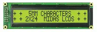
MC22405C6WK-SPTLY
Alphanumeric LCD, 24 x 2, Black on Yellow / Green, 5V, Parallel, English, Euro, Transflective
⚠️ Reference pricing provided. In case of supply shortages, we will connect you with our trusted procurement partners to ensure your project's continuity.
- Manufacturer: MIDAS
- Product type: Alphanumeric LCD Displays
- Font Set: English, Euro
- Module Size: 118mm x 36mm
- Display Mode: Transflective
- Logic Voltage: 5V
- Product Range: MC22405C6WK
- Character Size: 5.55mm
- Interface Type: Parallel
- LCD Display Type: STN
- Display Appearance: Black on Yellow / Green
- Backlighting Colour: Yellow / Green
- Display Construction: COB
- Character Count x Line: 24 x 2
- Operating Temperature Max: 70°C
- Operating Temperature Min: -20°C
| Delivery and price | |
|---|---|
| Units per pack | 10 |
| Price | 13.3 € |
| Current stock | 10+ |
| Lead time | 30 days |
Datasheet

**Midas Components Limited Telephone** +44 (0)1493 602602 Electra House **Fax** +44 (0)1493 665111 32 Southtown Road **Email** sales@midasdisplays.com Great Yarmouth **Website** www.midasdisplays.com Norfolk NR31 0DU England

**S ecification p** Part Number: ~~oe MC22405C6WK-SPTLY~~ Version: ~~a~~ Date: ~~a~~ **Revision No. Date Description Item Page** ~~IN git ‘Vs \ we,~~

BOOKBINDING AREA

## DOC.

## DATASHEET STATEMENT

**1.** The following icons are absolutely designed by Midas independently in 2007-SEP. They are not in common use in the LCD industry yet but just used for marking out Midas products’ characteristics quickly and simply without any special meaning. Midas reserves the composing right and copyright. No one else is allowed to adopt these icons without Midas approval.

**2.** The ISO9001 logo used in this document is authorized by SGS (www.sgs.com). Midas had already successfully passed the strict and professional ISO9001:2000 Quality Management System Certification and got the certificate (No.: CN07/00404)

**3.** The technologies/techniques/crafts which denoted by the following icons are not exclusively owned by Midas, but also shared by Midas LCD strategic cooperators, however all these technologies/techniques/crafts have been finally confirmed by Midas professional engineers and QC department.

**4.** As the difference in test standard and test conditions, also Midas insufficient familiarity with the actual LCD using environment, all the referred information in this DATASHEET (including the icons) only have two functions: 4.1: providing quick reference when you are judging whether or not the product meets your requirements. 4.2: listing out definitely the tolerance.

SAMPLE APPROVAL document rather than consider this DATASHEET as the standard for judging whether or not the LCD meets your requirements. Once you instruct Midas to a mass-production without definite demand for providing sample before, Midas will disclaim all responsibility if the mass-production is proved not meeting with your requirements.

**5.** The sequence of the icons is random and doesn’t indicate the importance grade.

**6.** Icons explanation

Midas 2006 version logo.Midas  is an integrated manufacturer of flat panel display (FPD). Midas supplies TN, HTN, STN, FSTN monochrome

LCD panel; COB, COG, TAB LCD module; and all kinds of LED backlight.

**FAST RESPONSE TIME** This icon on the cover indicates the product FFF is with high response speed; Otherwise not. 0 **HIGH CONTRAST** H C This icon on the cover indicates the product is with high contrast; Otherwise not. oF

## **PROTECTION CIRCUIT**

This icon on the cover indicates the product is with protection circuit; Otherwise not.

## **LONG LIFE VERSION**

This icon on the cover indicates the product is long life version (over 9K hours guaranteed); Otherwise not.

## **WIDE VIEWING SCOPE**

This icon on the cover indicates the product is with wide viewing scope; Otherwise not.

## **Anti UV VERSION**

UV This icon on the cover indicates the product is against UV line. Otherwise not.

## RoHS

## **RoHS COMPLIANCE**

This icon on the cover indicates the product meets ROHS requirements; Otherwise not.

## **OPERATION TEMPERATURE RANGE**

Y C

This icon on the cover indicates the operating X C temperature range (X-Y).

## **3TIMEs 100% QC EXAMINATION**

This icon on the cover indicates the product has passed Midas thrice 100% QC. Otherwise not.

## **TWICE SELECTION OF LED MATERIALS**

This icon on the cover indicates the LED had passed Midas twice strict selection which promises the product’s identical color and brightness; Otherwise not.

3.0V

## **Vlcm = 3.0V**

This icon on the cover indicates the product can work at 3.0V exactly; otherwise not.

N ™

## **N SERIES TECHNOLOGY (2008 developed)**

New structure, new craft, new technology and new materials inside both LCD module and LCD panel to improve the "RainBow"

## **MC22405C6WK-SPTLY**

## **Contents**

|_2._|_General Specification_|_Page 4_|
|---|---|---|
|_3._|_Module Classification Information_|_Page 5_|
|_4._|_Interface Pin Function_|_Page 6_|
|_5._|_Contour Drawing & Block Diagram_|_Page 7_|
|_6._|_Function Description_|_Page 8_|
|_7._|_Character Generator ROM Pattern_|_Page 11_|
|_8._|_Instruction Table_|_Page 12_|
|_9._|_Timing Characteristics_|_Page 13_|
|_10. Initializing of LCM_|_10. Initializing of LCM_|_Page 15_|
|_11. Optical Characteristics_|_11. Optical Characteristics_|_Page 17_|
|_12. Absolute Maximum Ratings_|_12. Absolute Maximum Ratings_|_Page 18_|
|_13. Electrical Characteristics_|_13. Electrical Characteristics_|_Page 18_|
|_14. Backlight Information_|_14. Backlight Information_|_Page 19_|
|_15. Reliability_|_15. Reliability_|_Page 20_|
|_16. Inspection specification_|_16. Inspection specification_|_Page 21_|
|_17._|_Precautions in use of LCD Modules_|_Page 25_|
|_18. Material List of Components for RoHs_|_18. Material List of Components for RoHs_<br>_Page 26_<br>designemanufactureesupply||


Page 2 , Total 28 Pages

## **2. General Specification**

The Features of the Module is description as follow:

Module dimension: 118.0 x 36.0 x 13.6 (max.) mm[3] View area: 94.5 x 16.0 mm[2] Active area: 88.3 x 11.5 mm[2] Number of Characters: 24 characters x 2 Lines Dot size: 0.6 x 0.65 mm[2] Dot pitch: 0.65 x 0.70 mm[2] Character size: 3.2 x 5.55 mm[2] Character pitch: 3.7 x 5.95 mm[2] LCD type: STN Positive, Yellow Green  Transflective Duty: 1/16 View direction: 6 o’clock Backlight Type: LED Yellow Green

Page 4 , Total 28 Pages

## **Midas LCD Part Number System**

**==> picture [479 x 28] intentionally omitted <==**

- 1 = **MC:** Midas Components

2

- = **Blank:** COB (chip on board) **COG** : chip on glass

3 = **No of dots** (e.g. 240064 = 240 x 64 dots) (e.g. 21605 = 2 x 16 5mm C.H.)

- 4 = **Series**

- 5 = **Series Variant:** A to Z **– see addendum**

6

7

8

- = **3:** 3 o’clock **6:** 6 o’clock **9** : 9 o’clock **12** : 12 o’clock

- = **S** : Normal (0 to + 50 deg C) **W:** Wide temp. (-20 to + 70 deg C) **X:** Extended temp (-30 + 80 Deg C)

- = **Character Set**

**Blank:** Standard (English/Japanese)

- **C:** Chinese Simplified (Graphic Displays only)

- **CB:** Chinese Big 5 (Graphic Displays only)

- **H:** Hebrew

- **K:** European (std) (English/German/French/Greek)

- **L:** English/Japanese (special)

- **M:** European (English/Scandinavian)

- **R:** Cyrillic

- **W:** European (English/Greek)

- **U:** European (English/Scandinavian/Icelandic)

9

- = **Bezel Height** (where applicable /available)

||Top of Bezel to Top<br>of PCB|LED Connection<br>Common (via pins 1<br>and 2)|Array or<br>Edge Lit|
|---|---|---|---|
|**Blank**|9.5mm / not<br>applicable|via pins 15+ 16-|Array|
|**2**|8.9 mm|Common|Array|
|**3**|7.8 mm|Separate|Array|
|**4**|7.8 mm|Common|Array|
|**5**|9.5 mm|Separate|Array|
|**6**|7 mm|Common|Array|
|**7**|7 mm|Separate|Array|
|**8**|6.4 mm|Common|Edge|
|**9**|6.4 mm|Separate|Edge|
|**A**|5.5 mm|Common|Edge|
|**B**|5.5 mm|Separate|Edge|
|**D**|6.0mm|Separate|Edge|
|**E**|5.0mm|Separate|Edge|
|**F**|4.7mm|Common|Edge|
|**G**|3.7mm|Separate|EL|
|**H**|7 mm|Separate|Edge|


- 10 = **T:** TN **S** : STN **B:** STN Blue **G:** STN Grey **F:** FSTN **F2:** FFSTN **V:** VA (Vertically Aligned)

- 11 = **P:** Positive **N** : Negative

- 12 = **R:** Reflective **M** : Transmissive **T:** Transflective

- 13 = **Backlight: Blank:** Reflective **L:** LED

- 14 = **Backlight Colour: Y:** Yellow-Green **W:** White **B:** Blue **R:** Red **A:** Amber **O:** Orange **G:** Green **RGB:** R.G.B.

15

16

= **Driver Chip: Blank:** Standard **I:** I[2] C **S** : SPI **T:** Toshiba T6963C **A:** Avant SAP1024B **R:** Raio RA6963 = **Voltage Variant** : e.g. **3** = 3v

F/Displays/Midas Brand/Midas LCD Part Number System 16 Oct 2013.doc

## **4. Interface Pin Function**

|**Pin No. Symbol**|**Pin No. Symbol**|**Level**|**Description**|
|---|---|---|---|
|1|VSS|0V|Ground|
|2|VDD|5.0V|Supply Voltage for logic|
|3|VO|(Variable) Operating voltage for LCD|(Variable) Operating voltage for LCD|
|4|RS|H/L|H: DATA, L: Instruction code|
|5|R/W|H/L|H: Read(MPU→Module) L: Write(MPU→Module)|
|6|E|H,H→L|Chip enable signal|
|7|DB0|H/L|Data bus line|
|8|DB1|H/L|Data bus line|
|9|DB2|H/L|Data bus line|
|10|DB3|H/L|Data bus line|
|11|DB4|H/L|Data bus line|
|12|DB5|H/L|Data bus line|
|13|DB6|H/L|Data bus line|
|14|DB7|H/L|Data bus line|
|15|A|-|Power supply for LED backlight ( + )|
|16|K|-|Power supply for LED backlight ( - )|


Page 6 , Total 28 Pages

## **5. Contour Drawing &Block Diagram**

Page 7 , Total 28 Pages

## **6. Function Description**

The LCD display Module is built in a LSI controller, the controller has two 8-bit registers, an instruction register (IR) and a data register (DR).

The IR stores instruction codes, such as display clear and cursor shift, and address information for display data RAM (DDRAM) and character generator (CGRAM). The IR can only be written from the MPU.  The DR temporarily stores data to be written or read from DDRAM or CGRAM.  When address information is written into the IR, then data is stored into the DR from DDRAM or CGRAM. By the register selector (RS) signal, these two registers can be selected.

**==> picture [397 x 98] intentionally omitted <==**

**----- Start of picture text -----**<br>
||||
|---|---|---|
|RS|R/W|Operation|
|0|0|IR write as an internal operation (display clear, etc.)|
|0|1|Read busy flag (DB7) and address counter (DB0 to DB7)|
|1|0|Write data to DDRAM or CGRAM (DR to DDRAM or CGRAM)|
|1|1|Read data from DDRAM or CGRAM (DDRAM or CGRAM to DR)|

**----- End of picture text -----**<br>


## **Busy Flag (BF)**

When the busy flag is 1, the controller LSI is in the internal operation mode, and the next instruction will not be accepted.  When RS=0 and R/W=1, the busy flag is output to DB7.  The next instruction must be written after ensuring that the busy flag is 0.

## **Address Counter (AC)**

The address counter (AC) assigns addresses to both DDRAM and CGRAM.

## **Display Data RAM (DDRAM)**

This DDRAM is used to store the display data represented in 8-bit character codes.  Its extended capacity is 80×8 bits or 80 characters.  Below figure is the relationships between DDRAM addresses and positions on the liquid crystal display.

**==> picture [467 x 100] intentionally omitted <==**

**----- Start of picture text -----**<br>
||||||||||||
|---|---|---|---|---|---|---|---|---|---|---|
|High bits|Low bits|
|Example: DDRAM addresses 4E|
||__| _____||
|AC|
|AC6 AC5|AC4 AC3|AC2 AC1|AC0|1|0|0|1|1|1|0|
|(hexadecimal)|
|PTET|TET)|LEE|ET|

**----- End of picture text -----**<br>


Page 8 , Total 28 Pages

Display position DDRAM address

1  2   3   4   5   6   7  ………………………  21  22  23  24 00 01 02 03 04 05 06 14 15 16 17 40 41 42 43 44 45 46 54 55 56 57 ~~oe~~ 2-Line by 24-Character Display

## **Character Generator ROM (CGROM)**

The CGROM generate 5×8 dot or 5×10 dot character patterns from 8-bit character codes. See Table 2.

## **Character Generator RAM (CGRAM)**

In CGRAM, the user can rewrite character by program.  For 5×8 dots, eight character patterns can be written, and for 5×10 dots, four character patterns can be written.

Write into DDRAM the character code at the addresses shown as the left column of table 1. To show the character patterns stored in CGRAM.

Page 9 , Total 28 Pages

## **Relationship between CGRAM Addresses, Character Codes (DDRAM) and Character patterns**

**Table 1.**

|F o r 5  *  8|F o r 5  *  8|F o r 5  *  8|F o r 5  *  8|F o r 5  *  8 d o t ch|F o r 5  *  8 d o t ch|d o t ch arac te r p att ern s|d o t ch arac te r p att ern s|d o t ch arac te r p att ern s|d o t ch arac te r p att ern s|arac te r p att ern s|arac te r p att ern s|||||||||||||||||||||
|---|---|---|---|---|---|---|---|---|---|---|---|---|---|---|---|---|---|---|---|---|---|---|---|---|---|---|---|---|---|---|---|
||||C h a rac ter C o d es<br>( D D R A M d a ta  )||||||||C G|R A|R A|M|A|d d res s|d d res s|d d res s||C h a rac ter Pa tte rn s<br>( C G|C h a rac ter Pa tte rn s<br>( C G R A M||||C h a rac ter Pa tte rn s<br> d at a )|||||||
|||7||6||5|4|3|2<br>0<br>1|||5|4||3|2|1|0||7|6||5|4||3|2|1|0|||
|||||H||ig h|L o w|L o w|L o w||H ig h          L o w|||ig h          L o w|ig h          L o w|ig h          L o w|ig h          L o w||||H ig h        L|||ig h        L|ig h        L|ig h        L o w|o w|||||
|||||||||||||||||0|0|0||*|*||*||||||0|||
|||||||||||||||||0|0|1||*|*||*|||0|0|0||||
|||0|||0|0|0|*|0<br>0<br>0|||0|0||0|0<br>0<br>1<br>1|1<br>1<br>0<br>0|0<br>1<br>0<br>1||*<br>*<br>*<br>*|*<br>*<br>*<br>*||*<br>*<br>*<br>*|||0<br>0<br>0|0<br>0|0<br>0|0<br>0<br>0||C h a rac ter<br>p att ern ( 1 )|
|||||||||||||||||1|1|0||*|*||*|||0|0|0||||
|||||||||||||||||1|1|1||*|*||*|0||0|0|0|0||C u rs o r p a tte rn|
|||||||||||||||||0|0|0||*|*||*|||0|0|0||||
|||||||||||||||||0|0|1||*|*||*|0|||0||0|||
|||||||||||||||||0|1|0||*|*||*|||||||||
|||||||||||||||||0|1|1||*|*||*|0||0||0|0||C h a rac ter|
||0|||0||0|0|*|0<br>0<br>1|||0|0||1|1|0|0||*|*||*||||||||p att ern ( 2 )|
|||||||||||||||||1|0|1||*|*||*|0||0||0|0|||
|||||||||||||||||1|1|0||*|*||*|0||0||0|0|||
|||||||||||||||||1|1|1||*|*||*|0||0|0|0|0||C u rs o r p a tte rn|
|||||||||||||||||0|0|0||*|*||*|||||||||
|||||||||||||||||0|0|1||||||||||||||
|||||||||||||||||||||||||||||||||
||0|||0||0|0|*|1<br>1<br>1|||1||1|1|1<br>1<br>1|0<br>0<br>1|0<br>1<br>0||||||||||||||
|||||||||||||||||1|1|1||*|*||*|||||||||
|F o r 5  *  1 0  d o t  ch a ract er p a tte rn s|F o r 5  *  1 0  d o t  ch a ract er p a tte rn s||F o r 5  *  1 0  d o t  ch a ract er p a tte rn s|||F o r 5  *  1 0  d o t  ch a ract er p a tte rn s||F o r 5  *  1 0  d o t  ch a ract er p a tte rn s||||||||||||||||||||||||
|C h a rac ter C o d es<br>( D D R A M d a ta  )<br>C G R A M A d d res s<br>C h a rac ter Pa tte rn s<br>( C G R A M d at a )<br>7<br>H ig h L o w<br>4<br>5<br>6<br>3<br>2<br>1<br>0<br>H ig h          L o w<br>5<br>4<br>3<br>2<br>1<br>0<br>H ig h          L o w<br>7<br>6<br>5<br>4<br>1<br>2<br>3<br>0<br>*<br>*<br>*<br>0<br>0<br>0<br>0<br>0<br>0<br>0<br>0<br>0<br>0<br>*<br>*<br>*<br>*<br>*<br>*<br>*<br>*<br>*<br>*<br>*<br>*<br>*<br>*<br>*<br>*<br>*<br>*<br>*<br>*<br>*<br>*<br>*<br>*<br>*<br>*<br>*<br>*<br>*<br>*<br>*<br>*<br>*<br>*<br>*<br>*<br>*<br>*<br>0<br>0<br>0<br>0<br>0<br>0<br>0<br>1<br>0<br>0<br>1<br>0<br>0<br>0<br>1<br>1<br>0<br>1<br>0<br>0<br>0<br>1<br>0<br>1<br>0<br>1<br>1<br>0<br>0<br>1<br>1<br>1<br>1<br>0<br>0<br>0<br>1<br>0<br>0<br>1<br>1<br>0<br>1<br>0<br>1<br>1<br>1<br>1<br>0<br>0<br>0<br>0<br>0<br>0<br>0<br>0<br>0<br>*<br>0<br>0<br>0<br>0<br>0<br>0<br>0<br>0<br>0<br>0<br>0<br>0<br>0<br>0<br>0<br>0<br>0<br>0<br>0<br>0<br>0<br>0<br>0<br>0<br>0<br>0<br>0<br>0<br>: " H ig h  "<br>mi~~:~~|||||||||||||||||||||||||||||||C h a rac ter<br>p att ern<br>C u rs o r p a tte rn|


Page 10 , Total 28 Pages

## **7. Character Generator ROM Pattern**

**Table 2.**

|Upper<br>4 bit<br>Lower<br>4 bit|LLLL||LLLH|LLLH|LLHL|LLHL|LLHL|LLHL|LLHL|LLHH|LLHH||LHLL|LHLL|LHLL|LHLL||LHLH|LHLH|LHLH|LHLH||LHHL|LHHL|LHHH|LHHH|LHHH|LHHH|LHHH|LHHH|HLLL|HLLL|HLLL|HLLL|HLLL|||HLLH|HLLH|HLLH|HLHL|HLHL|HLHL|HLHL||HLHH|HLHH|HLHH|HLHH|HHLL|HHLL|HHLL|HHLL|HHLL|HHLHHHHL|HHLHHHHL|HHHH|HHHH|
|---|---|---|---|---|---|---|---|---|---|---|---|---|---|---|---|---|---|---|---|---|---|---|---|---|---|---|---|---|---|---|---|---|---|---|---|---|---|---|---|---|---|---|---|---|---|---|---|---|---|---|---|---|---|---|---|---|---|---|
|LLLL|CG<br>RAM<br>( 1 )|||||||||i <br>he|<br> \||rs<br>:||||||||||||||||||||||||f||‘||||||||||||||||||||a<br>i.|
|LLLH|CG<br>RAM<br>( 2 )|||||||||sae<br>un<br>|]<br>t||||||||||||||1||||||<br>H|||||||1|||||||||||||||||||aly||atl||
||CG||||||||||||||||||||||||||||||||||||||||||||||||||||||||||
|LLHL|RAM<br>( 3 )||||||||||||||||||||||||||||||||||||||||||||||||||||||||||
||CG|||||||||\|||||||||||||||||||||||||||||||||||||||||||\|||i LI|||||
|LLHH<br>LHLL|RAM<br>( 4 )<br>CG<br>RAM<br>( 5 )||u|||Vu<br>}<br>=<br>ma<br>ae<br>Kenge<br>ae aha i||||||||||||||||||Y<br>|e||=x<br>ipower<br>i|||||||||wil<br>||||||caolillens<br> ee|||1|||||||||||||||H<br>iy<br>ZEEE <br>aan<br>Nan,<br>w||t<br> +|
|LHLH|CG<br>RAM<br>( 6 )||||||||||<br>Rafe:<br>"aan||||||||||||au<br>Placa<br>ae||||||a||:<br> te<br>"a|||||||||||||||H|besa"||||n*|||<br>Ts)<br>t||||ofa <br>i<br>]||im<br> a|
||CG||||||||||||||||||||||||||||||||||||||||||||||||||||||||||
|LHHL|RAM<br>( 7 )||||||||||||||||||||||||||||||||||||||||||||||||||||||||||
|LHHH|CG<br>RAM||||||||||||||||||||||||||||||||||||||||||||||||||||||||||
||( 8 )||||||||||||||||||||||||||||||||||||||||||||||||||||||||||
|HLLL|CG<br>RAM<br>( 1 )|||||||aa||eee|||||a||||||||||||||||||||||||ua||||||||||Ae|||||||ee||||
|HLLH|CG<br>RAM<br>( 2 )|||||“a,<br>zt<br>2”||||||||Tr<br>aie||||||||||||||||{|||||||HH||||||||||||||||||||'t<br>a“,<br>a<br>|||Lal<br>i<br>OE|
|HLHL|CG<br>RAM<br>( 3 )||||a|||||||||||||u|||||||||||||~||||||||||||||||||||||||aa|||Wu|
|HLHH|CG<br>RAM<br>( 4 )|||]||||||||!<br>mh|||||||1||||||||||||==||||||||||uJ i.<br>fiedt||||2<br> | ton ted||||||||||A||<br>: ™|||
||||:||||||||||||||||||||||||||||||||||||||||||||||||||||||||
|HHLL|CG<br>RAM<br>( 5 )|||||||||_<br>_|||||||||||||||||||||||||||||||ant.<br>PTs||||||||||||n||12s <br>aie,|—=<br> “ana,||<br>}|q|
|HHLH|CG<br>RAM<br>( 6 )|1||||||||||1||||||||||1||1|||||||i<br>aie||||||||||lenteneh tl<br>ma”|||||||.|||||||||1|vet|
||CG||||||||||||||||||||||||||||||||||||||||||||||||||||||||||
|HHHL|RAM<br>( 7 )|||||||||==||i||||||||||r||1||||||||||||1||||||||||||||||||||Renn"<br>||||
|HHHH|CG<br>RAM|||||||||=<br>2<br>.<br>1<br>**|**<br>!<br>H<br>an<br>1oie eed||||||||||||||||||||||||||||||||||||||||||||||||||
||( 8 )||||||||||||||||||||||||||||||||||||||||||||||||||||||||||


Page 11 , Total 28 Pages

## **8. Instruction Table**

|**Instruction**|**Instruction Code**|**Instruction Code**|**Instruction Code**|**Instruction Code**|**Instruction Code**|**Instruction Code**|**Instruction Code**|**Instruction Code**|**Instruction Code**|**Instruction Code**|RS R/W DB7 DB6 DB5 DB4 DB3 DB2 DB1 DB0<br>**Description**|**Execution time**<br>**(fosc=270Khz)**|
|---|---|---|---|---|---|---|---|---|---|---|---|---|
||RS R/W DB7 DB6 DB5 DB4 DB3 DB2 DB1 DB0|RS R/W DB7 DB6 DB5 DB4 DB3 DB2 DB1 DB0|RS R/W DB7 DB6 DB5 DB4 DB3 DB2 DB1 DB0|RS R/W DB7 DB6 DB5 DB4 DB3 DB2 DB1 DB0|RS R/W DB7 DB6 DB5 DB4 DB3 DB2 DB1 DB0|RS R/W DB7 DB6 DB5 DB4 DB3 DB2 DB1 DB0|RS R/W DB7 DB6 DB5 DB4 DB3 DB2 DB1 DB0|RS R/W DB7 DB6 DB5 DB4 DB3 DB2 DB1 DB0|RS R/W DB7 DB6 DB5 DB4 DB3 DB2 DB1 DB0|RS R/W DB7 DB6 DB5 DB4 DB3 DB2 DB1 DB0|||
|Clear Display|Clear Display<br>0|0|0|0|0|0|0|0|0|1|Write “00H” to DDRAM and set<br>DDRAM address to “00H” from AC|1.53ms|
|Return Home|0|0|0|0|0|0|0|0|1|-|Set DDRAM address to “00H” from AC<br>and return cursor to its original position<br>if shifted. The contents of DDRAM are<br>not changed.|1.53ms|
|Entry Mode<br>Set|0|0|0|0|0|0|0|1|I/D|SH|Assign cursor moving direction and<br>enable the shift of entire display.|39μs|
|Display<br>ON/OFF<br>Control|0|0|0|0|0|0|1|D|C|B|Set display (D), cursor (C), and blinking<br>of cursor (B) on/off control bit.|39μs|
|Cursor or<br>Display Shift|0|0|0|0|0|1|S/C R/L|S/C R/L|-|-|Set cursor moving and display shift<br>control bit, and the direction, without<br>changingof DDRAM data.|39μs|
|Function Set|0|0|0|0|1|DL|N|F|-|-|Set interface data length<br>(DL:8-bit/4-bit), numbers of display line<br>(N:2-line/1-line)and, display font type<br>(F:5×11 dots/5×8 dots)|(DL:8-bit/4-bit), numbers of display line<br>39μs|
|Set CGRAM<br>Address|0|0|0|1|AC5 AC4 AC3 AC2 AC1 AC0|AC5 AC4 AC3 AC2 AC1 AC0|AC5 AC4 AC3 AC2 AC1 AC0|AC5 AC4 AC3 AC2 AC1 AC0|AC5 AC4 AC3 AC2 AC1 AC0|AC5 AC4 AC3 AC2 AC1 AC0|AC5 AC4 AC3 AC2 AC1 AC0Set CGRAM address in address counter.|39μs|
|Set DDRAM<br>Address|0|0|1|AC6 AC5 AC4 AC3 AC2 AC1 AC0|AC6 AC5 AC4 AC3 AC2 AC1 AC0|AC6 AC5 AC4 AC3 AC2 AC1 AC0|AC6 AC5 AC4 AC3 AC2 AC1 AC0|AC6 AC5 AC4 AC3 AC2 AC1 AC0|AC6 AC5 AC4 AC3 AC2 AC1 AC0|AC6 AC5 AC4 AC3 AC2 AC1 AC0|AC6 AC5 AC4 AC3 AC2 AC1 AC0Set DDRAM address in address counter.|Set DDRAM address in address counter.<br>39μs|
|Read Busy<br>Flag and<br>Address|0|1|BF AC6 AC5 AC4 AC3 AC2 AC1 AC0|BF AC6 AC5 AC4 AC3 AC2 AC1 AC0|BF AC6 AC5 AC4 AC3 AC2 AC1 AC0|BF AC6 AC5 AC4 AC3 AC2 AC1 AC0|BF AC6 AC5 AC4 AC3 AC2 AC1 AC0|BF AC6 AC5 AC4 AC3 AC2 AC1 AC0|BF AC6 AC5 AC4 AC3 AC2 AC1 AC0|BF AC6 AC5 AC4 AC3 AC2 AC1 AC0|BF AC6 AC5 AC4 AC3 AC2 AC1 AC0<br>Whether during internal operation or not<br>can be known by reading BF. The<br>contents of address counter can also be<br>read.|Whether during internal operation or not<br>0μs|
|Write Data to<br>RAM|Write Data to<br>1|0|D7|D6|D5|D4|D3|D2|D1|D0|Write data into internal RAM<br>(DDRAM/CGRAM).|43μs|
|Read Data<br>from RAM|1|1|D7|D6|D5|D4|D3|D2|D1|D0|Read data from internal RAM<br>(DDRAM/CGRAM).|43μs|


* ”-”:don’t care

Page 12 , Total 28 Pages

## **9. Timing Characteristics**

**9.1 Write Operation**

|VIH1<br>VIL1<br>VIH1<br>VIL1<br>VIL1<br>tcycE<br>VIH1<br>VIL1<br>VIH1<br>VIL1<br>VIL1<br>tAS<br>tAH<br>tAH<br>tEf<br>tH<br>tDSW<br>PWEH<br>tEr<br>VIL1<br>VIH1<br>VIL1<br>VIH1<br>VIL1<br>RS<br>R/W<br>E<br>DB0 to DB7<br>Valid data<br>~~eee~~|VIH1<br>VIL1<br>VIH1<br>VIL1<br>VIL1<br>tcycE<br>VIH1<br>VIL1<br>VIH1<br>VIL1<br>VIL1<br>tAS<br>tAH<br>tAH<br>tEf<br>tH<br>tDSW<br>PWEH<br>tEr<br>VIL1<br>VIH1<br>VIL1<br>VIH1<br>VIL1<br>RS<br>R/W<br>E<br>DB0 to DB7<br>Valid data<br>~~eee~~|VIH1<br>VIL1<br>VIH1<br>VIL1<br>VIL1<br>tcycE<br>VIH1<br>VIL1<br>VIH1<br>VIL1<br>VIL1<br>tAS<br>tAH<br>tAH<br>tEf<br>tH<br>tDSW<br>PWEH<br>tEr<br>VIL1<br>VIH1<br>VIL1<br>VIH1<br>VIL1<br>RS<br>R/W<br>E<br>DB0 to DB7<br>Valid data<br>~~eee~~|VIH1<br>VIL1<br>VIH1<br>VIL1<br>VIL1<br>tcycE<br>VIH1<br>VIL1<br>VIH1<br>VIL1<br>VIL1<br>tAS<br>tAH<br>tAH<br>tEf<br>tH<br>tDSW<br>PWEH<br>tEr<br>VIL1<br>VIH1<br>VIL1<br>VIH1<br>VIL1<br>RS<br>R/W<br>E<br>DB0 to DB7<br>Valid data<br>~~eee~~|VIH1<br>VIL1<br>VIH1<br>VIL1<br>VIL1<br>tcycE<br>VIH1<br>VIL1<br>VIH1<br>VIL1<br>VIL1<br>tAS<br>tAH<br>tAH<br>tEf<br>tH<br>tDSW<br>PWEH<br>tEr<br>VIL1<br>VIH1<br>VIL1<br>VIH1<br>VIL1<br>RS<br>R/W<br>E<br>DB0 to DB7<br>Valid data<br>~~eee~~|VIH1<br>VIL1<br>VIH1<br>VIL1<br>VIL1<br>tcycE<br>VIH1<br>VIL1<br>VIH1<br>VIL1<br>VIL1<br>tAS<br>tAH<br>tAH<br>tEf<br>tH<br>tDSW<br>PWEH<br>tEr<br>VIL1<br>VIH1<br>VIL1<br>VIH1<br>VIL1<br>RS<br>R/W<br>E<br>DB0 to DB7<br>Valid data<br>~~eee~~|VIH1<br>VIL1<br>VIH1<br>VIL1<br>VIL1<br>tcycE<br>VIH1<br>VIL1<br>VIH1<br>VIL1<br>VIL1<br>tAS<br>tAH<br>tAH<br>tEf<br>tH<br>tDSW<br>PWEH<br>tEr<br>VIL1<br>VIH1<br>VIL1<br>VIH1<br>VIL1<br>RS<br>R/W<br>E<br>DB0 to DB7<br>Valid data<br>~~eee~~|VIH1<br>VIL1<br>VIH1<br>VIL1<br>VIL1<br>tcycE<br>VIH1<br>VIL1<br>VIH1<br>VIL1<br>VIL1<br>tAS<br>tAH<br>tAH<br>tEf<br>tH<br>tDSW<br>PWEH<br>tEr<br>VIL1<br>VIH1<br>VIL1<br>VIH1<br>VIL1<br>RS<br>R/W<br>E<br>DB0 to DB7<br>Valid data<br>~~eee~~|VIH1<br>VIL1<br>VIH1<br>VIL1<br>VIL1<br>tcycE<br>VIH1<br>VIL1<br>VIH1<br>VIL1<br>VIL1<br>tAS<br>tAH<br>tAH<br>tEf<br>tH<br>tDSW<br>PWEH<br>tEr<br>VIL1<br>VIH1<br>VIL1<br>VIH1<br>VIL1<br>RS<br>R/W<br>E<br>DB0 to DB7<br>Valid data<br>~~eee~~|VIH1<br>VIL1<br>VIH1<br>VIL1<br>VIL1<br>tcycE<br>VIH1<br>VIL1<br>VIH1<br>VIL1<br>VIL1<br>tAS<br>tAH<br>tAH<br>tEf<br>tH<br>tDSW<br>PWEH<br>tEr<br>VIL1<br>VIH1<br>VIL1<br>VIH1<br>VIL1<br>RS<br>R/W<br>E<br>DB0 to DB7<br>Valid data<br>~~eee~~|VIH1<br>VIL1<br>VIH1<br>VIL1<br>VIL1<br>tcycE<br>VIH1<br>VIL1<br>VIH1<br>VIL1<br>VIL1<br>tAS<br>tAH<br>tAH<br>tEf<br>tH<br>tDSW<br>PWEH<br>tEr<br>VIL1<br>VIH1<br>VIL1<br>VIH1<br>VIL1<br>RS<br>R/W<br>E<br>DB0 to DB7<br>Valid data<br>~~eee~~|VIH1<br>VIL1<br>VIH1<br>VIL1<br>VIL1<br>tcycE<br>VIH1<br>VIL1<br>VIH1<br>VIL1<br>VIL1<br>tAS<br>tAH<br>tAH<br>tEf<br>tH<br>tDSW<br>PWEH<br>tEr<br>VIL1<br>VIH1<br>VIL1<br>VIH1<br>VIL1<br>RS<br>R/W<br>E<br>DB0 to DB7<br>Valid data<br>~~eee~~|VIH1<br>VIL1<br>VIH1<br>VIL1<br>VIL1<br>tcycE<br>VIH1<br>VIL1<br>VIH1<br>VIL1<br>VIL1<br>tAS<br>tAH<br>tAH<br>tEf<br>tH<br>tDSW<br>PWEH<br>tEr<br>VIL1<br>VIH1<br>VIL1<br>VIH1<br>VIL1<br>RS<br>R/W<br>E<br>DB0 to DB7<br>Valid data<br>~~eee~~|VIH1<br>VIL1<br>VIH1<br>VIL1<br>VIL1<br>tcycE<br>VIH1<br>VIL1<br>VIH1<br>VIL1<br>VIL1<br>tAS<br>tAH<br>tAH<br>tEf<br>tH<br>tDSW<br>PWEH<br>tEr<br>VIL1<br>VIH1<br>VIL1<br>VIH1<br>VIL1<br>RS<br>R/W<br>E<br>DB0 to DB7<br>Valid data<br>~~eee~~|VIH1<br>VIL1<br>VIH1<br>VIL1<br>VIL1<br>tcycE<br>VIH1<br>VIL1<br>VIH1<br>VIL1<br>VIL1<br>tAS<br>tAH<br>tAH<br>tEf<br>tH<br>tDSW<br>PWEH<br>tEr<br>VIL1<br>VIH1<br>VIL1<br>VIH1<br>VIL1<br>RS<br>R/W<br>E<br>DB0 to DB7<br>Valid data<br>~~eee~~|VIH1<br>VIL1<br>VIH1<br>VIL1<br>VIL1<br>tcycE<br>VIH1<br>VIL1<br>VIH1<br>VIL1<br>VIL1<br>tAS<br>tAH<br>tAH<br>tEf<br>tH<br>tDSW<br>PWEH<br>tEr<br>VIL1<br>VIH1<br>VIL1<br>VIH1<br>VIL1<br>RS<br>R/W<br>E<br>DB0 to DB7<br>Valid data<br>~~eee~~|VIH1<br>VIL1<br>VIH1<br>VIL1<br>VIL1<br>tcycE<br>VIH1<br>VIL1<br>VIH1<br>VIL1<br>VIL1<br>tAS<br>tAH<br>tAH<br>tEf<br>tH<br>tDSW<br>PWEH<br>tEr<br>VIL1<br>VIH1<br>VIL1<br>VIH1<br>VIL1<br>RS<br>R/W<br>E<br>DB0 to DB7<br>Valid data<br>~~eee~~|||
|---|---|---|---|---|---|---|---|---|---|---|---|---|---|---|---|---|---|---|
|||||||||||||Ta=25|Ta=25|Ta=25|Ta=25|Ta=25℃, VDD=5.0± 0.5V|||
|Item|||||||Symbol||Min|||Typ|||Max|||Unit|
|Enable cycle time|||||||tcycE||1200|||-|||-|||ns|
|Enable pulse width (high level)||Enable pulse width (high level)|Enable pulse width (high level)||||PWEH||140|||-|||-|||ns|
|Enable rise/fall time|||||||tEr,tEf|||-||-|||25|||ns|
|Address set-up time (RS, R/W to E)||Address set-up time (RS, R/W to E)||Address set-up time (RS, R/W to E)|Address set-up time (RS, R/W to E)||tAS|||0||-|||-|||ns|
|Address hold time|||||||tAH|||10||-|||-|||ns|
|Data set-up time|||||||tDSW|||40||-|||-|||ns|
|Data hold time|||||||tH|||10||-|||-|||ns|


Page 13 , Total 28 Pages

**9.2 Read Operation**

|VIH1<br>VIL1<br>VIH1<br>VIL1<br>tcycE<br>VOH1<br>VOL1*<br>tAS<br>tAH<br>tAH<br>tEf<br>tDHR<br>PWEH<br>tEr<br>VIL1<br>VIH1<br>VIL1<br>VIH1<br>VIL1<br>RS<br>R/W<br>E<br>DB0 to DB7<br>VIH1<br>VIH1<br>VOH1<br>*VOL1<br>Valid data<br>tDDR<br>a~~aes~~|VIH1<br>VIL1<br>VIH1<br>VIL1<br>tcycE<br>VOH1<br>VOL1*<br>tAS<br>tAH<br>tAH<br>tEf<br>tDHR<br>PWEH<br>tEr<br>VIL1<br>VIH1<br>VIL1<br>VIH1<br>VIL1<br>RS<br>R/W<br>E<br>DB0 to DB7<br>VIH1<br>VIH1<br>VOH1<br>*VOL1<br>Valid data<br>tDDR<br>a~~aes~~|VIH1<br>VIL1<br>VIH1<br>VIL1<br>tcycE<br>VOH1<br>VOL1*<br>tAS<br>tAH<br>tAH<br>tEf<br>tDHR<br>PWEH<br>tEr<br>VIL1<br>VIH1<br>VIL1<br>VIH1<br>VIL1<br>RS<br>R/W<br>E<br>DB0 to DB7<br>VIH1<br>VIH1<br>VOH1<br>*VOL1<br>Valid data<br>tDDR<br>a~~aes~~|VIH1<br>VIL1<br>VIH1<br>VIL1<br>tcycE<br>VOH1<br>VOL1*<br>tAS<br>tAH<br>tAH<br>tEf<br>tDHR<br>PWEH<br>tEr<br>VIL1<br>VIH1<br>VIL1<br>VIH1<br>VIL1<br>RS<br>R/W<br>E<br>DB0 to DB7<br>VIH1<br>VIH1<br>VOH1<br>*VOL1<br>Valid data<br>tDDR<br>a~~aes~~|VIH1<br>VIL1<br>VIH1<br>VIL1<br>tcycE<br>VOH1<br>VOL1*<br>tAS<br>tAH<br>tAH<br>tEf<br>tDHR<br>PWEH<br>tEr<br>VIL1<br>VIH1<br>VIL1<br>VIH1<br>VIL1<br>RS<br>R/W<br>E<br>DB0 to DB7<br>VIH1<br>VIH1<br>VOH1<br>*VOL1<br>Valid data<br>tDDR<br>a~~aes~~|VIH1<br>VIL1<br>VIH1<br>VIL1<br>tcycE<br>VOH1<br>VOL1*<br>tAS<br>tAH<br>tAH<br>tEf<br>tDHR<br>PWEH<br>tEr<br>VIL1<br>VIH1<br>VIL1<br>VIH1<br>VIL1<br>RS<br>R/W<br>E<br>DB0 to DB7<br>VIH1<br>VIH1<br>VOH1<br>*VOL1<br>Valid data<br>tDDR<br>a~~aes~~|VIH1<br>VIL1<br>VIH1<br>VIL1<br>tcycE<br>VOH1<br>VOL1*<br>tAS<br>tAH<br>tAH<br>tEf<br>tDHR<br>PWEH<br>tEr<br>VIL1<br>VIH1<br>VIL1<br>VIH1<br>VIL1<br>RS<br>R/W<br>E<br>DB0 to DB7<br>VIH1<br>VIH1<br>VOH1<br>*VOL1<br>Valid data<br>tDDR<br>a~~aes~~|VIH1<br>VIL1<br>VIH1<br>VIL1<br>tcycE<br>VOH1<br>VOL1*<br>tAS<br>tAH<br>tAH<br>tEf<br>tDHR<br>PWEH<br>tEr<br>VIL1<br>VIH1<br>VIL1<br>VIH1<br>VIL1<br>RS<br>R/W<br>E<br>DB0 to DB7<br>VIH1<br>VIH1<br>VOH1<br>*VOL1<br>Valid data<br>tDDR<br>a~~aes~~|VIH1<br>VIL1<br>VIH1<br>VIL1<br>tcycE<br>VOH1<br>VOL1*<br>tAS<br>tAH<br>tAH<br>tEf<br>tDHR<br>PWEH<br>tEr<br>VIL1<br>VIH1<br>VIL1<br>VIH1<br>VIL1<br>RS<br>R/W<br>E<br>DB0 to DB7<br>VIH1<br>VIH1<br>VOH1<br>*VOL1<br>Valid data<br>tDDR<br>a~~aes~~|VIH1<br>VIL1<br>VIH1<br>VIL1<br>tcycE<br>VOH1<br>VOL1*<br>tAS<br>tAH<br>tAH<br>tEf<br>tDHR<br>PWEH<br>tEr<br>VIL1<br>VIH1<br>VIL1<br>VIH1<br>VIL1<br>RS<br>R/W<br>E<br>DB0 to DB7<br>VIH1<br>VIH1<br>VOH1<br>*VOL1<br>Valid data<br>tDDR<br>a~~aes~~|VIH1<br>VIL1<br>VIH1<br>VIL1<br>tcycE<br>VOH1<br>VOL1*<br>tAS<br>tAH<br>tAH<br>tEf<br>tDHR<br>PWEH<br>tEr<br>VIL1<br>VIH1<br>VIL1<br>VIH1<br>VIL1<br>RS<br>R/W<br>E<br>DB0 to DB7<br>VIH1<br>VIH1<br>VOH1<br>*VOL1<br>Valid data<br>tDDR<br>a~~aes~~|VIH1<br>VIL1<br>VIH1<br>VIL1<br>tcycE<br>VOH1<br>VOL1*<br>tAS<br>tAH<br>tAH<br>tEf<br>tDHR<br>PWEH<br>tEr<br>VIL1<br>VIH1<br>VIL1<br>VIH1<br>VIL1<br>RS<br>R/W<br>E<br>DB0 to DB7<br>VIH1<br>VIH1<br>VOH1<br>*VOL1<br>Valid data<br>tDDR<br>a~~aes~~|VIH1<br>VIL1<br>VIH1<br>VIL1<br>tcycE<br>VOH1<br>VOL1*<br>tAS<br>tAH<br>tAH<br>tEf<br>tDHR<br>PWEH<br>tEr<br>VIL1<br>VIH1<br>VIL1<br>VIH1<br>VIL1<br>RS<br>R/W<br>E<br>DB0 to DB7<br>VIH1<br>VIH1<br>VOH1<br>*VOL1<br>Valid data<br>tDDR<br>a~~aes~~|VIH1<br>VIL1<br>VIH1<br>VIL1<br>tcycE<br>VOH1<br>VOL1*<br>tAS<br>tAH<br>tAH<br>tEf<br>tDHR<br>PWEH<br>tEr<br>VIL1<br>VIH1<br>VIL1<br>VIH1<br>VIL1<br>RS<br>R/W<br>E<br>DB0 to DB7<br>VIH1<br>VIH1<br>VOH1<br>*VOL1<br>Valid data<br>tDDR<br>a~~aes~~|VIH1<br>VIL1<br>VIH1<br>VIL1<br>tcycE<br>VOH1<br>VOL1*<br>tAS<br>tAH<br>tAH<br>tEf<br>tDHR<br>PWEH<br>tEr<br>VIL1<br>VIH1<br>VIL1<br>VIH1<br>VIL1<br>RS<br>R/W<br>E<br>DB0 to DB7<br>VIH1<br>VIH1<br>VOH1<br>*VOL1<br>Valid data<br>tDDR<br>a~~aes~~|VIH1<br>VIL1<br>VIH1<br>VIL1<br>tcycE<br>VOH1<br>VOL1*<br>tAS<br>tAH<br>tAH<br>tEf<br>tDHR<br>PWEH<br>tEr<br>VIL1<br>VIH1<br>VIL1<br>VIH1<br>VIL1<br>RS<br>R/W<br>E<br>DB0 to DB7<br>VIH1<br>VIH1<br>VOH1<br>*VOL1<br>Valid data<br>tDDR<br>a~~aes~~|VIH1<br>VIL1<br>VIH1<br>VIL1<br>tcycE<br>VOH1<br>VOL1*<br>tAS<br>tAH<br>tAH<br>tEf<br>tDHR<br>PWEH<br>tEr<br>VIL1<br>VIH1<br>VIL1<br>VIH1<br>VIL1<br>RS<br>R/W<br>E<br>DB0 to DB7<br>VIH1<br>VIH1<br>VOH1<br>*VOL1<br>Valid data<br>tDDR<br>a~~aes~~|VIH1<br>VIL1<br>VIH1<br>VIL1<br>tcycE<br>VOH1<br>VOL1*<br>tAS<br>tAH<br>tAH<br>tEf<br>tDHR<br>PWEH<br>tEr<br>VIL1<br>VIH1<br>VIL1<br>VIH1<br>VIL1<br>RS<br>R/W<br>E<br>DB0 to DB7<br>VIH1<br>VIH1<br>VOH1<br>*VOL1<br>Valid data<br>tDDR<br>a~~aes~~|||
|---|---|---|---|---|---|---|---|---|---|---|---|---|---|---|---|---|---|---|---|
|NOTE: *VOL1 is assumed to be 0.8V at 2 MHZ operation.|NOTE: *VOL1 is assumed to be 0.8V at 2 MHZ operation.|||NOTE: *VOL1 is assumed to be 0.8V at 2 MHZ operation.||NOTE: *VOL1 is assumed to be 0.8V at 2 MHZ operation.|NOTE: *VOL1 is assumed to be 0.8V at 2 MHZ operation.|||||||||||||
|Ta=25℃,VDD=5.0± 0.5V||||||||||||||||||||
|Item||||||Symbol|||Min||||Typ||Max||||Unit|
|Enable cycle time||||||||tcycE|1200||||-||-||||ns|
|Enable pulse width (high level)|||||||PWEH||140||||-||-||||ns|
|Enable rise/fall time|||||||tEr,tEf||-||||-||25||25||ns|
|Address set-up time (RS, R/W to E)||Address set-up time (RS, R/W to E)||Address set-up time (RS, R/W to E)||||tAS|0||||-||-||||ns|
|Address hold time||||||||tAH|10||||-||-||||ns|
|Data delay time||||||||tDDR|-||||-||100||||ns|
|Data hold time||||||||tDHR|10||||-||-||||ns|


Ta=25℃, VDD=5.0± 0.5V

Page 14 , Total 28 Pages

## **10. Initializing of LCM**

**==> picture [372 x 546] intentionally omitted <==**

**----- Start of picture text -----**<br>
Power on<br>Wait for more than 40 ms after VDD rises to 4.5 V<br>BF can not be checked before this instruction.<br>RS R/W DB7 DB6 DB5 DB4 DB3 DB2 DB1 DB0 Function set<br>0 0 0 0 1 1 * * * *<br>Wait for more than 39us<br>BF can not be checked before this instruction.<br>RS R/W DB7 DB6 DB5 DB4 DB3 DB2 DB1 DB0<br>Function set<br>0 0 0 0 1 0 * * * *<br>0 0 N F * * * * * *<br>Wait for more than 39  µ s<br>BF can not be checked before this instruction.<br>RS R/W DB7 DB6 DB5 DB4 DB3 DB2 DB1 DB0<br>0 0 0 0 1 0 * * * * Function set<br>0 0 N F * * * * * *<br>Wait for more than 37us<br>RS R/W DB7 DB6 DB5 DB4 DB3 DB2 DB1 DB0 Display ON/OFF control<br>0 0 0 0 0 0 * * * *<br>0 0 1 D C B * * * *<br>Wait for more than 37  µ s<br>RS R/W DB7 DB6 DB5 DB4 DB3 DB2 DB1 DB0<br>0 0 0 0 0 0 * * * *  Display Clear<br>0 0 0 0 0 1 * * * *<br>Wait for more than 1 .53 ms<br>RS R/W DB7 DB6 DB5 DB4 DB3 DB2 DB1 DB0<br>Entry Mode Set<br>0 0 0 0 0 0 * * * *<br>0 0 0 1 I/D SH * * * *<br>Initialization ends<br>**----- End of picture text -----**<br>


4-Bit Ineterface

Page 15 , Total 28 Pages

**==> picture [435 x 567] intentionally omitted <==**

**----- Start of picture text -----**<br>
Power on<br>Ga<br>Wait for more than 40 ms after VDD rises to 4.5 V<br>BF can not be checked before this instruction.<br>— — —_<br>RS R/WDB7 DB6 DB5 DB4 DB3 DB2 DB1 DB0 Function set<br>—— 0 0 0 0 1 1 N F * *<br>_———<br>Wait for more than 39us<br>po<br>BF can not be checked before this instruction.<br>Oo RS R/WDB7 DB6 DB5 DB4 DB3 DB2 DB1 DB0 Po<br>Function set<br>0 0 0 0 1 1 N F * *<br>_——<br>Wait for more than 37us<br>nN Al<br>e RS R/WDB7 DB6 DB5 s DB4 DB3 DB2 DB1 DB0<br>Display ON/OFF control<br>oY 2<br>0 0 0 0 0 0 1 B C D<br>Ae ee<br>Wait for more than 37  µ s<br>[design » mani<br>O RS R/WDB7 DB6 DB5 o DB4 DB3 DB2 DB1 DB0<br> Display Clear<br>0 0 0 0 0 0 0 0 0 1<br>_——<br>Wait for more than 1 .53 ms<br>po<br>O RS R/WDB7 DB6 DB5 o DB4 DB3 DB2 DB1 DB0<br>Entry Mode Set<br>pe 0 0 0 0 0 0 0 1 I/D S<br>Initialization ends<br>po<br>**----- End of picture text -----**<br>


8-Bit Ineterface

Page 16 , Total 28 Pages

## **11. Optical Characteristics**

|**Item**|**Symbol**|**Symbol**<br>**Condition**|**Min**|**Typ**|**Max**|**Unit**|
|---|---|---|---|---|---|---|
|View Angle|(V)θ|CR≧2|20|-|40|deg|
||(H)φ|CR≧2|-30|-|30|deg|
|Contrast Ratio|CR|-|-|3|-|-|
|Response Time|T rise|-|-|200|300|ms|
||T fall|-|-|200|300|ms|


## **Definition of Operation Voltage (Vop)         Definition of Response Time ( Tr , Tf )**

**==> picture [428 x 168] intentionally omitted <==**

**----- Start of picture text -----**<br>
Non-selected Non-selected<br>Intensity Selected Wave Conition Selected Conition Conition<br>100% Non-selected Wave<br>Intensity<br>10%<br>Cr Max<br>Cr = Lon / Loff 90%<br>100%<br>Vop<br>Driving Voltage(V) Tr Tf<br>[positive type] [positive type]<br>**----- End of picture text -----**<br>


**==> picture [93 x 10] intentionally omitted <==**

**----- Start of picture text -----**<br>
Conditions :<br>**----- End of picture text -----**<br>


Operating Voltage : Vop Viewing Angle(θ,φ) : 0°, 0° Frame Frequency : 64 HZ Driving Waveform : 1/N duty , 1/a bias **Definition of viewing angle(CR** ≧ **2)**

**==> picture [290 x 172] intentionally omitted <==**

**----- Start of picture text -----**<br>
θ b<br>θ f °<br>φ= 180<br>θl<br>θr<br>φ= 270° φ= 90°<br>φ= 0°<br>**----- End of picture text -----**<br>


Page 17 , Total 28 Pages

**12. Absolute Maximum Ratings**

**Item Symbol Min Typ Max Unit** Operating Temperature TOP -20 - +70 ℃ Storage Temperature TST -30 - +80 ℃ Input Voltage VI VSS - VDD V Supply Voltage For Logic VDD-VSS -0.3 - 7 V Supply Voltage For LCD VDD-V0 -0.3 - 13 V ~~ae~~ **13. Electrical Characteristics**

|**Item**|**Symbol**|**Condition**|**Min**|**Typ**|**Max**|**Unit**|
|---|---|---|---|---|---|---|
|Supply Voltage For Logic|VDD-VSS|-|4.5|5.0|5.5|V|
|Supply Voltage For LCD|VDD-V0|Ta=-20℃<br>Ta=25℃<br>Ta=+70℃|-<br>-<br>3.8|-<br>4.5<br>-|5.5<br>-<br>-|V<br>V<br>V|
|Input High Volt.|VIH|-|0.7 VDD|-|VDD|V|
|Input Low Volt.|VIL|-|VSS|-|0.6|V|
|Output High Volt.|VOH|-|3.9|-|-|V|
|Output Low Volt.|VOL|-|-|-|0.4|V|
|Supply Current|IDD|VDD=5V|1.0|1.2|1.5|mA|


Page 18 , Total 28 Pages

## **14. Backlight Information**

## **Specification**

|**PARAMETER**<br>~~a~~<br>~~es~~|**SYMBOL**<br>~~ee~~<br>~~ee~~|**MIN**<br>~~ee~~<br>~~ee~~|**TYP**<br>~~ee~~<br>~~ee~~|**MAX**<br>~~ee~~<br>~~ee~~|**UNIT**<br>~~ee~~|**TEST** **CONDITION**<br>~~ee~~<br>~~ee~~|
|---|---|---|---|---|---|---|
|**Supply Current**<br>~~a ~~<br>~~es~~<br>~~po~~|**ILED**<br> ~~ee~~<br>~~ee~~|**28.8**<br>~~ee~~<br>~~ee~~|**32**<br>~~ee~~<br>~~ee~~|**50**<br>~~ee~~<br>~~ee~~|**mA**<br>~~ee ~~|**V=3.5V**<br> ~~ee~~<br>~~ee~~|
|**Supply Voltage **<br>~~es ~~<br>~~po~~<br>~~a~~|**V**<br> ~~ee ~~<br>~~ee~~|**3.4**<br> ~~ee ~~<br>~~ee~~|**3.5**<br> ~~ee~~<br>~~ee~~|**3.6**<br>~~ee~~<br>~~ee~~|**V**<br>~~ee~~|~~ee~~<br>~~eee~~|
|**Reverse Voltage **<br>~~po~~<br>~~a~~<br>~~ee~~|**VR**<br>~~ee~~<br>~~ee~~|-<br>~~ee~~<br>~~ee~~|**5**<br>~~ee~~|-<br>~~ee~~<br>~~ee~~|**V**<br>~~ee~~<br>~~ee~~|~~eee~~<br>~~eee~~|
|**Luminous Intensity**<br>~~a ~~<br>~~ee~~<br>~~ee~~<br>~~ee~~|**IV**<br> ~~ee~~<br>~~ee~~<br>~~ee~~<br>~~ee~~|**210**<br>~~ee~~<br>~~ee~~<br>~~ee~~|**230**<br>~~ee~~<br>~~ee~~|-<br>~~ee~~<br>~~ee~~<br>~~ee~~|**CD/M2**<br>~~ee ~~<br>~~ee~~<br>~~ee~~|**ILED=32mA**<br> ~~eee~~<br>~~eee~~<br>~~ee~~<br>~~ee~~|
|**Wave Length**<br>~~ee ~~<br>~~ee~~<br>~~ee~~<br>~~|~~|λ**p**<br> ~~ee~~<br>~~ee~~<br>~~ee~~|~~ee~~<br>~~ee~~|~~ee~~|~~ee~~<br>~~ee~~<br>~~eee~~|**nm**<br>~~ee ~~<br>~~ee~~<br>~~eee~~|**ILED=32mA**<br> ~~eee~~<br>~~ee~~<br>~~ee~~<br>~~eee~~|
|**Life Time**<br>~~ee ~~<br>~~ee~~<br>~~|~~<br>~~NIL~~|~~ee~~<br>~~ee~~<br>~~NILAL~~|- **100**<br>~~ee~~<br>~~AL~~|**100K **<br>~~ee~~|-<br>~~ee~~<br>~~eee~~|**Hr.**<br>~~ee~~<br>~~eee~~|**ILED=32mA**<br>~~ee~~<br>~~ee~~<br>~~eee~~|
|**Color**<br>~~|~~<br>~~NIL~~|**White**<br>~~eee~~<br>~~NILAL~~<br>~~N/V~~||||||


2.D rive from pin15,pin16

**==> picture [106 x 59] intentionally omitted <==**

**----- Start of picture text -----**<br>
R R<br>A<br>B/L<br>K<br>“E LCM E<br>ill never get Vee output from pin15)<br>**----- End of picture text -----**<br>


Page 19 , Total 28 Pages

## **15. Reliability**

**Content of Reliability Test (wide temperature, -20** ℃ **~70** ℃ **)**

|**Content of Reliability Test (wide temperature, -20y Test (wide temperature, -20 Test (wide temperature, -20(wide temperature, -20wide temperature, -20perature, -20erature, -20, -20 -20**℃**~70**℃**)**|**Content of Reliability Test (wide temperature, -20y Test (wide temperature, -20 Test (wide temperature, -20(wide temperature, -20wide temperature, -20perature, -20erature, -20, -20 -20**℃**~70**℃**)**|**Content of Reliability Test (wide temperature, -20y Test (wide temperature, -20 Test (wide temperature, -20(wide temperature, -20wide temperature, -20perature, -20erature, -20, -20 -20**℃**~70**℃**)**|**Content of Reliability Test (wide temperature, -20y Test (wide temperature, -20 Test (wide temperature, -20(wide temperature, -20wide temperature, -20perature, -20erature, -20, -20 -20**℃**~70**℃**)**|
|---|---|---|---|
|**Environmental Test**||||
|**Test Item**|**Content of Test**|**Test Condition**|**Note**|
|High Temperature storage|Endurance test applying the high storage temperature for a long<br>time.|Endurance test applying the high storage temperature for a long<br>80℃<br>200hrs|2|
|Low Temperature<br>storage|Endurance test applying the high storage temperature for a long<br>time.|Endurance test applying the high storage temperature for a long<br>-30℃<br>200hrs|1,2|
|High Temperature<br>Operation|Endurance test applying the electric stress (Voltage & Current)<br>and the thermal stress to the element for a long time.|Endurance test applying the electric stress (Voltage & Current)<br>70℃<br>200hrs|——|
|Low Temperature<br>Operation|Endurance test applying the electric stress under low temperature<br>for a long time.|Endurance test applying the electric stress under low temperature<br>-20℃<br>200hrs|1|
|High Temperature/<br>Humidity Operation|The module should be allowed to stand at 60<br>,90%RH max<br>℃<br>For 96hrs under no-load condition excluding the polarizer,<br>Then taking it out and drying it at normal temperature.|60<br>,90%RH<br>℃<br>96hrs|1,2|
|Thermal shock resistance|The sample should be allowed stand the following 10 cycles of<br>operation<br>-20℃25<br>℃<br>70℃<br>30min   5min    30min<br>1 cycle|-20<br>/<br>℃70℃<br>10 cycles|——|
|Vibration test|Endurance test applying the vibration during transportation and<br>using.|Endurance test applying the vibration during transportation and<br>Total fixed amplitude :<br>15mm<br>Vibration<br>Frequency<br>:<br>10~55Hz<br>One cycle 60 seconds to 3<br>directions of X,Y,Z for<br>Each 15 minutes|Total fixed amplitude :<br>:<br>One cycle 60 seconds to 3<br>directions of X,Y,Z for<br>3|
|Static electricity test|Endurance test applying the electric stress to the terminal.|VS=800V,RS=1.5kΩ<br>CS=100pF<br>1 time|——|


**Note1: No dew condensation to be observed.**

**Note2: The function test shall be conducted after 4 hours storage at the normal Temperature and humidity after remove from the test chamber. Note3: Vibration test will be conducted to the product itself without putting it in a container.**

Page 20 , Total 28 Pages

## **16. Inspection specification**

|NO<br>~~fT~~|Item<br>~~fT~~|Criterion<br>~~fT~~|AQL<br>~~fT~~|
|---|---|---|---|
|01<br>~~fT~~|Electrical<br>Testing<br>~~fT~~|1.1 Missing vertical, horizontal segment, segment contrast defect.<br>1.2 Missing character , dot or icon.<br>1.3 Display malfunction.<br>1.4 No function or no display.<br>1.5 Current consumption exceeds product specifications.<br>1.6 LCD viewing angle defect.<br>1.7 Mixed product types.<br>1.8 Contrast defect.<br>~~fT~~|0.65<br>~~fT~~|
|02|Black or white<br>spots on LCD<br>(display only)|2.1 White and black spots on display≦0.25mm, no more than<br>three white or black spots present.<br>2.2 Densely spaced: No more than two spots or lines within 3mm|2.5|
|03|LCD black<br>spots, white<br>spots,<br>contamination<br>(non-display)|3.1 Round type : As<br>following drawing<br>Φ=( x + y ) / 2<br>SIZE<br>Acceptable Q<br>TY<br>Φ≦0.10<br>Accept no dense<br>0.10<Φ≦0.20<br>2<br>0.20<Φ≦0.25<br>1<br>0.25<Φ<br>0<br>~~S|~~|2.5<br>~~S|~~|
|||3.2 Line type : (As followingdrawing)<br>Length<br>Width<br>AcceptableQTY<br>---<br>W≦0.02<br>Accept no dense<br>L≦3.0<br>0.02<W≦0.03<br>L≦2.5<br>0.03<W≦0.05<br>2<br>---<br>0.05<W<br>As round type<br>~~|~~|2.5<br>~~|~~|
|04|Polarizer<br>bubbles|If bubbles are visible,<br>judge using black spot<br>specifications, not easy<br>to find, must check in<br>specify direction.<br>Size Φ<br>AcceptableQTY<br>Φ≦0.20<br>Accept no dense<br>0.20<Φ≦0.50<br>3<br>0.50<Φ≦1.00<br>2<br>1.00<Φ<br>0<br>Total Q TY<br>3|2.5|


Page 21 , Total 28 Pages

**==> picture [486 x 608] intentionally omitted <==**

**----- Start of picture text -----**<br>
a NO  Item   a ee Criterion  AQL<br>a 05  Scratches  Follow NO.3 LCD black spots, white spots, contamination<br>Symbols Define:<br>x: Chip length      y: Chip width     z: Chip thickness<br>k: Seal width       t: Glass thickness  a: LCD side length<br>L: Electrode pad length:<br>6.1 General glass chip :<br>6.1.1 Chip on panel surface and crack between panels:<br>K<br>k<br>SN<br>z: Chip thickness  y: Chip width  x: Chip length<br>Z≦1/2t  Not over viewing  x≦1/8a<br>06  Chipped  area  2.5<br>glass<br>1/2t<z≦2t  Not exceed 1/3k   x≦1/8a<br>☉If there are 2 or more chips, x is total length of each chip.<br>6.1.2 Corner crack:<br>z: Chip thickness  y: Chip width  x: Chip length<br>Z≦1/2t  Not over viewing  x≦1/8a<br>area<br>1/2t<z≦2t  Not exceed 1/3k   x≦1/8a<br>☉If there are 2 or more chips, x is the total length of each chip.<br>**----- End of picture text -----**<br>


Page 22 , Total 28 Pages

**==> picture [486 x 578] intentionally omitted <==**

**----- Start of picture text -----**<br>
a NO  Item   a ee Criterion  AQL<br>Symbols :<br>x: Chip length      y: Chip width     z: Chip thickness<br>k: Seal width       t: Glass thickness  a: LCD side length<br>L: Electrode pad length<br>6.2 Protrusion over terminal :<br>6.2.1 Chip on electrode pad :<br>Z<br>y: Chip width   x: Chip length  z: Chip thickness<br>y≦0.5mm  x≦1/8a  0  < z ≦ t<br>6.2.2 Non-conductive portion:<br>i L<br>Glass<br>06  2.5<br>crack<br>te z Me eae OE d<br>A A<br>y: Chip width   x: Chip length  z: Chip thickness<br>y≦ L  x≦1/8a  0  < z ≦ t<br>☉If the chipped area touches the ITO terminal, over 2/3 of the ITO<br>must remain and be inspected according to electrode terminal<br>specifications.<br>☉If the product will be heat sealed by the customer, the alignment<br>mark not be damaged.<br>6.2.3 Substrate protuberance and internal crack.<br>x<br>y: width   x: length<br>y≦1/3L  x ≦ a<br>**----- End of picture text -----**<br>


Page 23 , Total 28 Pages

|NO<br>~~a~~|Item|Criterion|AQL|
|---|---|---|---|
|07|Cracked glass|The LCD with extensive crack is not acceptable.|2.5|
|08|Backlight<br>elements|8.1 Illumination source flickers when lit.<br>8.2 Spots or scratched that appear when lit must be judged. Using<br>LCD spot, lines and contamination standards.<br>8.3 Backlight doesn’t light or color wrong.|0.65<br>2.5<br>0.65|
|09|Bezel|9.1 Bezel may not have rust, be deformed or have fingerprints,<br>stains or other contamination.<br>9.2 Bezel must complywithjob specifications.|2.5<br>0.65|
|10|PCB、COB|10.1 COB seal may not have pinholes larger than 0.2mm or<br>contamination.<br>10.2 COB seal surface may not have pinholes through to the IC.<br>10.3 The height of the COB should not exceed the height indicated<br>in the assembly diagram.<br>10.4 There may not be more than 2mm of sealant outside the seal<br>area on the PCB. And there should be no more than three<br>places.<br>10.5 No oxidation or contamination PCB terminals.<br>10.6 Parts on PCB must be the same as on the production<br>characteristic chart. There should be no wrong parts, missing<br>parts or excess parts.<br>10.7 The jumper on the PCB should conform to the product<br>characteristic chart.<br>10.8 If solder gets on bezel tab pads, LED pad, zebra pad or screw<br>hold pad, make sure it is smoothed down.<br>10.9 The Scraping testing standard for Copper Coating of PCB<br>**Y**<br>**X**<br> **X * Y<=2mm2**|2.5<br>2.5<br>0.65<br>2.5<br>2.5<br>0.65<br>0.65<br>2.5<br>2.5|
|11|Soldering|11.1 No un-melted solder paste may be present on the PCB.<br>11.2 No cold solder joints, missing solder connections, oxidation<br>or icicle.<br>11.3 No residue or solder balls on PCB.<br>11.4 No short circuits in components on PCB.|2.5<br>2.5<br>2.5<br>0.65|


Page 24 , Total 28 Pages

|NO|Item|Criterion|AQL|
|---|---|---|---|
|12|General<br>appearance|12.1 No oxidation, contamination, curves or, bends on interface<br>Pin (OLB) of TCP.<br>12.2 No cracks on interface pin (OLB) of TCP.<br>12.3 No contamination, solder residue or solder balls on product.<br>12.4 The IC on the TCP may not be damaged, circuits.<br>12.5 The uppermost edge of the protective strip on the interface<br>pin must be present or look as if it cause the interface pin to<br>sever.<br>12.6 The residual rosin or tin oil of soldering (component or chip<br>component) is not burned into brown or black color.<br>12.7 Sealant on top of the ITO circuit has not hardened.<br>12.8 Pin type must match type in specification sheet.<br>12.9 LCD pin loose or missing pins.<br>12.10 Product packaging must the same as specified on packaging<br>specification sheet.<br>12.11 Product dimension and structure must conform to product<br>specification sheet.|2.5<br>0.65<br>2.5<br>2.5<br>2.5<br>2.5<br>2.5<br>0.65<br>0.65<br>0.65<br>0.65|


## **17. Precautions in use of LCD Modules**

(1)Avoid applying excessive shocks to the module or making any alterations or modifications to it.

(2)Don’t make extra holes on the printed circuit board, modify its shape or change the components of LCD module.

(3)Don’t disassemble the LCM.

(4)Don’t operate it above the absolute maximum rating.

(5)Don’t drop, bend or twist LCM.

(6)Soldering: only to the I/O terminals.

(7)Storage: please storage in anti-static electricity container and clean environment.

Page 25 , Total 28 Pages

## **18. Material List of Components for RoHs**

1. Midas Components Ltd. hereby declares that all of or part of products, including, but not limited to, the LCM, accessories or packages, manufactured and/or delivered to your company (including your subsidiaries and affiliated company) directly or indirectly by our company (including our subsidiaries or affiliated companies) do not intentionally contain any of the substances listed in all applicable EU directives and regulations, including the following substances.

Exhibit A : The Harmful Material List Material (Cd) (Pb) (Hg) (Cr6+) PBBs PBDEs Limited 100 1000 1000 1000 1000 1000 Value ppm ppm ppm ppm ppm ppm ~~Pere~~ Above limited value is set up according to RoHS. 2.Process for RoHS requirement : (1) Use the Sn/Ag/Cu soldering surface ; the surface of Pb-free solder is rougher than we used before.

- (2) Heat-resistance temp. :

   - Reflow : 250 ℃ ,30 seconds Max. ; Connector soldering wave or hand soldering : 320 ℃ , 10 seconds max.

- (3) Temp. curve of reflow, max. Temp. : 235±5 ℃;

   - Recommended customer’s soldering temp. of connector : 280 ℃ , 3 seconds.

Page 26 , Total 28 Pages
Updated at February 9, 2023
About Novapart
Novapart is a B2B electronic component broker specialising in stock shortages and cost reduction. We source hard-to-find parts and identify compliant alternatives across a catalogue of 410,000+ components from 500+ manufacturers.
Learn more →Stock Shortage Specialist
When a component is unavailable, discontinued or has an unacceptable lead time, we tap into our network of vetted European and Asian distributors to source what you need — without compromising on quality or traceability.
Request a quote →Compliant Alternatives
We identify pin-to-pin, electrically equivalent substitutes that meet the same certifications (RoHS, AEC-Q100, REACH) as your original specification — validated against datasheets, not just part numbers. Often at a lower cost.
BOM Analysis service →