
Image not available
Illustrative purposes only

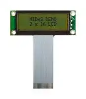
MC21603A6W-SPR-V2
Alphanumeric LCD, 16 x 2, Black on Yellow / Green, 5V, Parallel, English, Japanese, Reflective
⚠️ Reference pricing provided. In case of supply shortages, we will connect you with our trusted procurement partners to ensure your project's continuity.
- Manufacturer: MIDAS
- Product type: Alphanumeric LCD Displays
- Font Set: English, Japanese
- Module Size: 53mm x 20mm
- Display Mode: Reflective
- Logic Voltage: 5V
- Product Range: MC21603A
- Character Size: 3.15mm
- Interface Type: Parallel
- LCD Display Type: STN
- Display Appearance: Black on Yellow / Green
- Display Construction: COB
- Character Count x Line: 16 x 2
- Operating Temperature Max: 70°C
- Operating Temperature Min: -20°C
| Delivery and price | |
|---|---|
| Units per pack | 250 |
| Price | 6.19 € |
| Current stock | 200+ |
| Lead time | 7 days |
Datasheet

Electra House, 32 Southtown Road Great Yarmouth, Norfolk \ NR31 ODU, England

Telephone +44 (0)1493 602602 Fax +44 (0)1493 665111 Email:sales@midasdisplays.com www.midasdisplays.com

**==> picture [83 x 54] intentionally omitted <==**

**----- Start of picture text -----**<br>
f A.<br>| f—><br>t / \<br>Displays<br>**----- End of picture text -----**<br>


**==> picture [519 x 375] intentionally omitted <==**

**----- Start of picture text -----**<br>
MC21603A6W-SPR-V2 3mm Character Height LCD Module<br>Specification<br>Date: 28/10/2020<br>Display Features<br>Character Count<br>Blackon Yellow/Green<br>Logic Voltage<br>Parallel<br>Font Set English / Japanese Ro tal S<br>Display Mode Reflective li rt<br>Character Height compgan<br>LC Type<br>Module Size 53.00 x 20.00 x 8.00mm<br>Operating Temperature -20°C ~ +70°C<br>LED Backlight eeeeeBox Quantity | Weightee / Displayeee<br>**----- End of picture text -----**<br>


> * - For full design functionality, please use this specification in conjunction with the ST7066U specification. (Provided Separately)

**==> picture [116 x 13] intentionally omitted <==**

**----- Start of picture text -----**<br>
Display Accessories<br>**----- End of picture text -----**<br>


**==> picture [243 x 30] intentionally omitted <==**

**----- Start of picture text -----**<br>
Optional Variants<br>| Fonts| Appearances | Voltage<br>**----- End of picture text -----**<br>


## 1. FUNCTIONS & FEATURES

- @ MC21603A6W-SPR-V2 Series LCD type : e Viewing Direction : 6 O’clock @ Driving Scheme : 1/16 e Power Supply Voltage :5.0V e LCD Operation Voltage :4.6V e Display contents : 16 e Internal Memory : CGROM

   - : 1/16 Duty, 1/5 Bias

   - : 16 Characters x 2 line : CGROM (13200bits )

   - : CGRAM (64 x 8bits) : DDRAM (80 x 8 bits for Digits) : CGROM of the ST7066U-0A

. CGROM @ 8-Bit Parallel e RoHS Compliant

## 2. MECHANICAL SPECIFICATIONS

**==> picture [393 x 83] intentionally omitted <==**

**----- Start of picture text -----**<br>
@ Module Size - 53.00(L) x20.00(W) x 8.00(H)mni<br>® Viewing area : 36.00(L) x10.00 (W) mm<br>® Active area : 34.10(L) x 7.40(W) mm<br>. Dot Size > 0.33 (L) x 0.35 (W) mm<br>® Dot Gap : 0.05mm<br>**----- End of picture text -----**<br>


## EXTERNAL DIMENSIONS

**==> picture [425 x 626] intentionally omitted <==**

**----- Start of picture text -----**<br>
2) 3/15<br>N(| °PR +0.05 ui<br>ear ey ee<br>HH E>) n<br>0.35 o SS<br>g Oo | Oo fe 3.15<br>alo | [| _ 4.25<br>af al a<br>2 —| | rarer<br>j=}<br>jo} i}<br>O°! O-<br>|<br>Ss = nD re)<br>$|2 3 5 5 6<br>s|3\g a 2 8<br>oo) | oS a) 3<br>—<br>———a A<br>10.00<br>Ye, 5 ° ©<br>yey » N) cy C<br>I © O<br>Q..0 “ieOT yr<br>LA prea g|2|# n= Oo<br>S|| 8]of Sl |<ele |aa ET , —= Oo —O<br>| SE | ° 5.00 — oD) i<br>90)aamb 0 S Oo:~ 5S O_<br>3) 8) 8/8 | eae<br>A Ol Po A/A 7.40 A x 5<br>5.00 " | || V/A 10.00 YG =<br>2.50 Lis.0020.215.00+0.2 =ome<br>20.00+0.5 44,00+1 c c=<br>3 <=<br>Kr NW)<br>**----- End of picture text -----**<br>


## BLOCK DIAGRAM

**==> picture [489 x 385] intentionally omitted <==**

**----- Start of picture text -----**<br>
VSS<br>V0 =oy) CUM1-CUMI6 2line*16characters<br>RS —»> F Noa)<br>R/W No)<br>7 >"| _ =)MN<br>© - SEG1~SEG40 SEG41~SEG80<br>DO~D/ aa<br>SG“ | CONTROL SIGNALS ST 7065<br>PIN ASSIGNMENT<br>H:Read(Module><br>P66 | CE [ChipenablesignahMPU) L: (MPU>Module)<br>ee ee)<br>ee<br>**----- End of picture text -----**<br>


## MAXIMUM ABSOLUTE POWER RATINGS

|Supply voltage for|logic|Symbol||Standardvalue||
|---|---|---|---|---|---|
|Supply voltage forLCD|LCD|||||
|Operating temperature||||-20~+70||
|DC CHARACTERISTICS||||||
|Supply<br>Voltage For<br>PP”<br>Logic|Vpp-Vss||5.0||V|
|Supply Voltage For|||_||V|
|LED|Voo-Vo||4.6||Vv|
|*Note|||7||V|


## DC CHARACTERISTICS

* Note: Please design the VOP adjustment circuit on customer's main board

A VSS 10K~20K vss _| Module vr aed

## AC CHARACTERISTICS

## 1. Write mode

**==> picture [436 x 94] intentionally omitted <==**

**----- Start of picture text -----**<br>
Vin<br>RS VII<br>RW \ /<br>**----- End of picture text -----**<br>


## 2. Read Mode

**==> picture [517 x 130] intentionally omitted <==**

**----- Start of picture text -----**<br>
||||||||||||||||
|---|---|---|---|---|---|---|---|---|---|---|---|---|---|---|
|EnableCycleTime|||te|||200|||||~|[ons|||EB|
|Enable|Pulse|Time|||Tow =||to|||~|[||~|||om|||EF|||
|Enable|Rise/Fall Time|||Te Te|||—~|||~|[||25|[|ms|||EB|
|Address Set-up|Time|||Tas,|(||0|||=|||Ts|||RWRSE|
|Address|HoldTime|||Ton|||10|||||||ts|||RWRSE|
|DataSetupTime|||Toor|||~|||~|||100|||ns|||DBo-DB7|
|DataHoldTime|||ST|||to|||||~|||as|||Bo-a7_|

**----- End of picture text -----**<br>


**==> picture [9 x 7] intentionally omitted <==**

**----- Start of picture text -----**<br>
°<br>**----- End of picture text -----**<br>


## STANDARD CHARACTER PATTERN (ST7066U-0A)

NO.? 066-04 eso] 00000001] o010f0071]orenforos]o0 ort frao0 00 ras0 or frrao fos [into frat (1) pooh | (IIE FI | |RIEIRIE oo! |ERISA |ERIE eo] | BRIA IESE] pon]poo] ol IRI EIBIE) | | **|** EG IEIEPIRIEAPEHIRE 0104| ©) i a Poasa] i ee west fat aBEE| RSS pen] E: zs | roo} oT[EeTSTEESE]SS tie | [PF eS ee VARS] poor | SRE Eee ool] | BAIR g ronfo] | IEE PRIREIALE roll EVERIEIE (S| | [AIF |EIB |B RSA] rolo! | PRIA ee | Ileal IRIE fol SE el | ENEE aRs IBa

## INSTRUCTION TABLE

|Command | RS |R/W|Command | RS |R/W|[DB7/DB6|DB5|DB4]|[DB7/DB6|DB5|DB4]|DB3 |DB2 |DBI | DBo|EXecutlontime<br>(fosc=270KHz)|DB3 |DB2 |DBI | DBo|EXecutlontime<br>(fosc=270KHz)|DB3 |DB2 |DBI | DBo|EXecutlontime<br>(fosc=270KHz)|DB3 |DB2 |DBI | DBo|EXecutlontime<br>(fosc=270KHz)|DB3 |DB2 |DBI | DBo|EXecutlontime<br>(fosc=270KHz)|Remark|
|---|---|---|---|---|---|---|---|---|---|
|Clear<br>Display|||||||I|152<br>ems|Write”20H” toDDRAM.And set<br>DDRAMaddress to“00H”fromAC|
||||||||||SetDDRAM address to “OOH” fromAC|
|Betonhome||||||1|x|Sains|and return cursorto its original position if<br>shifted.The contents ofDDRAM arenot|
||||||||||changed.|
|Ent<br>4<br>nz _ ©<br>°|||||1|V/D|Ss|37us|Sets cursor move direction and specifies<br>display<br>shift.<br>These<br>operations<br>are<br>performed during data writeand read.|
|Display|||||||||D=1: entire display on|
|on/off<br>0|(0)||0|1|D|¢||37us|C=1: cursoron|
|control|||||||||B=1: cursorposition on|
|Cursor|||||||||Set cursor moving and display shift|
|or|||1|S/C | R/L||x|x|37us|control bit, and the direction, without|
|Display Shift|||||||||changingDDRAM data.|
|function<br>Set|||1 |DL]|N|F|x|x|37us|DL: interfacedata is 8/4 bits<br>N: numberofline is2/1<br>F: font size is 5x11/5x8|
|Readbusy|||||||||Whether during internal operation or not|
|flag&|1|BF|JAC6]ACS]AC4||AC3 |AC2 |ACI |ACO||||Ous|can beknownby reading BF. The contents|
|address|||||||||ofaddress counter can also be read.|
|Write data|||||||||Write data into internalRAM|
|Read data|||||||||Read data from internal RAM (DDRAM /|
|Note:||||||||||


Be sure the ST7066U is not in the busy state (BF=00 before sending an instruction from the MPU to the ST7066U. If an instruction is sent without checking the busy flag, the time between the first instruction and next instruction will take much longer than the instruction time itself. Refer to instruction table for the list of each instruction execution time.

## RESET FUNCTION

## 8-bit Interface (fosc=270KHz)

**==> picture [67 x 8] intentionally omitted <==**

**----- Start of picture text -----**<br>
After Veo =4_5Y<br>**----- End of picture text -----**<br>


_———Fanetion set cee 1 this instruction. Spree ee [~~ pisplaywattsONIOFF ans[contro] i [Rows [oeess[osa[oesjos]oe%|oe0 po}olofololol1}olc]es| Waite ars oispaay i cea [wpa oeeoss[osa[oesjosz]oe%|oe0 Folo}lololololofolol}a Wattine ans erry [as mode sat po[fololo}ololo}s] nw[os7[o8e)oss[osq[oss[osz/os[os0iw} s| oe

## 4-bit Interface (fosc=270KHz)

Wait time >40m5S AfterWoo >4_5

| ——CFunctionset ' BFcannctbe | [RS [RW]DB7[066[0B5[DB4[DB3[0B2[DB1[DB0| *--------7 checked before | Fofolofo{[+a][+|{[x|[x|[x[x| | this instruction.|

Foftoloflo{[+ajo|x|x|[x[x|

eae|

**==> picture [5 x 14] intentionally omitted <==**

**----- Start of picture text -----**<br>
|<br>**----- End of picture text -----**<br>


Fol @lolol1{o|x lx [x[x S esinetintint. | To [go [w lr [x ]x|x [x [x[x] Ras snnaseeos-RS[[RIW]DB7|D66[DB5[D54|[DB3[D62|061/DB0)] Display ON/OFF control Fotololofojo|x|/[x|{x[x| fotol[1s{folelelx|[x{[x[x]

[RS [RIW[DB7|D66[085[D54|DB3[D62|081/DB0| fofololofofo|x|x|x[x| Fofololofola|[x [xx [x] Rs[[RW]0B7|D66[085[DB4[DB3[062|DB1/DB0)] Entry mode set Foftofoflofofo|{x|x|/x|[x_ fofolol1{w]s|[x][x[x[x]

**==> picture [348 x 264] intentionally omitted <==**

**----- Start of picture text -----**<br>
DISPLAY L=41.5+0.2 1.0 MAX<br>0.5+0.5 POLARIZER L=40.5+0.3<br>2.25-+ MIN VIEWING AREA L=37.0———+ --0.2140.05<br>3.7 ACTIVE AREA L=34,1-—-———___+ 0.7+0.05<br>1.95 PITCH 0.8X47=37.6 0.7+40.05<br>| a —Ah°0.4TTTTYP -1+0.4 TYP 48 I0.26+0.05<br>oon | | | |<br>eeBHPSST]| | HH HY HH HHeeSARAH eeleee|<br>plead} 1 ii fo) S)<br>===Sa I } ee a eee eee |alo fe ES<br>ast LI | SEEEE HERE esl ELEC HEE ETT SHEE HEE rE ERLE EE eH EEE ses<br>Bae |i 143<br>| a TTS)<<br>}N bdg fomte) b of+ —ll-o.4————P]TCHTYP 0.8X17=37.60.4 TYP |K-1.95<br>w<br>N<br>UNLESS OTHERWISE SPECIFIED<br>DIMENSIONS ARE IN MM<br>TOLERANCES:+0.2MM<br>| Se |<br>| PETE |<br>SO UTI<br>(1:1)<br>**----- End of picture text -----**<br>


**==> picture [373 x 256] intentionally omitted <==**

**----- Start of picture text -----**<br>
5.4]<br>LO<br>w<br>Ty TT<br>1 {0.3 !<br>1 —80000 00000 00000 00000 00090 00000 00009 09009 6009 09909 0000 6000 0009 000 00000 Oooo T<br>IR | SPEER| LAEEEREOO000  EEEOOoEEH EEEEHEEEO00 GOODE HEEEEE EEEEHGSCHEE EEREGooEEE SEESBooEEE [H]  EEECOEEE HEHE EEECOOPSESS ERYDEOEEEH CerEOD0OEEE SED SOScheeESSHEHE  Peo coeHEE S008HEH ceeDSop8EEE  ceDApeHE ||| N~-<br>||| —T ERE QOO00QO0D0 QO00DODODECOO GO000COD0DCO60 GO000OOOOOOOO 90000BOCDOOD O00COO08COONS GOOCS DODEO GoOOC>CODEDCOD) GooGOOCOO Bo0o>DeeDCO C009G08CODD G08GOD0DOOO 8o000OODOO) GooCOO0oCOD Oooo9DooboOOO OOO OoooDoor 1|I N<|<br>1 ERE ECHR EEEEH EEEEH EEEEH EEE EEE EEE EEE EEC EEE EEE HEH EH EE iS<br>1 EEE EERE EEE HELE EEEEE EEE EERE EEE EECEH EECEH EEE EEE EEE EEE EE EY | CN<br>C1 ICO OOO OO000 OOOO OOOO CD09 OSD0 COO Ge GSS C0 0 OO C0 OoooOO t xs<br>R16 PITCH 2.18X16-0,3=34,t "84<br>iB<br>= sss sata wo<br>27 | [ 49<br>a<br>UNLESS OTHERWISE SPECIFIED<br>DIMENSIONS ARE IN MM<br>TOLERANCES: +0.2MM<br>**----- End of picture text -----**<br>


## PAD CONFIGURATION & GRAPHIC DIMENSION

**==> picture [463 x 374] intentionally omitted <==**

**----- Start of picture text -----**<br>
2.15<br>PAD _NO. PAD CONFIGURATION<br>21 COM 87 [R 87 (C1—C80)| 185K-0.33<br>| | rH D4<br>8 COM1[R1(C1—C80)] 5D See Ht<br>9 SEG21[C21(R1—R16)] 2" OOOO Oe<br>| io 6 > LULL Uo<br>| SN Oooo o<br>28 SEG40[C40(R1—R16)] ~ | Goon L]<br>29 SEG61[C61(R1—R16)] LILI<br>| |<br>48 SEG80[C80(R1—R16)] qooco o<br>49 COM9[R9(C1—C80)] 0.05<br>:<br>56<br>COM 16[R16(41-c80), ' UNLESS OTHERWISE SSPECIFIED<br>| L<br>76 SECMMC41(RTER16)] i .<br>77 SEG20[C20(RTR16)1 )<br>| |<br>96 SEG1[61(R1—R16)]<br>**----- End of picture text -----**<br>


SEG & COM LAYOUT

SEG21 SEG40 SEG61 sae) TMNT LUNUAUOACUANUAUACUAUUATEAEATE®

ee eee ee eeei

| ee

OP TALL UTA UTLUTLAT UTTER SEG20. SEG41 SEG60 06 2

SEG1

SEG LAYOUL COM8 COMI TIMI LUNUAUUAUINUI TIES

MMT **|** _HEEEE EEEe eeyep eye ee SSCP Eee EEE EET EERIE

**|**

a ePUUTAVTA VTA UTAUTAUUAUA TATA TAA UAUUAUUAUHAUIEL:9 96 COM16 COM9

COM LAYOUT

## THE MODULE ACCEPT QUALITY LEVEL (AQL)

1. Inspection Standard: ANSI Z-1.4 Table Normal Inspection Single Sampling Level II.

## RELIABILITY TEST

Operating life time: 50,000 hours

(at room temperature without direct irradiation of sunlight) Reliability characteristics shall meet following requirements.

|Tests Item||
|---|---|
|.<br>Hightemperature storage|+80"<br>80°C x96HRS|
||“30°C x4HRS|
||-20°C x4HRS|
|Hightemperature, Highhumidity|°<br>0<br>‘TRH<br>2BSPa oeDiSIRS|
|Thermal shock|=20°'@x30min> 25°C x 10s De#70°CRBOmin<br>x 5 cycles|
|ae<br>Vibrationtest|Frequency x SwingxTime<br>A0Hzx4mmx 4hrs|
||Dropheight*Times|


## QUALITY DESCRIPTION & APPLICATION NOTE

Please refer to “General Inspection Criteria” document
Updated at February 9, 2023
About Novapart
Novapart is a B2B electronic component broker specialising in stock shortages and cost reduction. We source hard-to-find parts and identify compliant alternatives across a catalogue of 410,000+ components from 500+ manufacturers.
Learn more →Stock Shortage Specialist
When a component is unavailable, discontinued or has an unacceptable lead time, we tap into our network of vetted European and Asian distributors to source what you need — without compromising on quality or traceability.
Request a quote →Compliant Alternatives
We identify pin-to-pin, electrically equivalent substitutes that meet the same certifications (RoHS, AEC-Q100, REACH) as your original specification — validated against datasheets, not just part numbers. Often at a lower cost.
BOM Analysis service →