


MC21205A6W1-SPTLY
Alphanumeric LCD, 12 x 2, Black on Yellow / Green, 5V, Parallel, English, Japanese, Transflective
- Manufacturer: MIDAS DISPLAYS
- Product type: Alphanumeric LCD Displays
- Character Count x Line:12 x 2; Display Appearance:Black on Yellow / Green; Logic Voltage:5V; Interface Type:Parallel; Font Set:English, Japanese; Display Mode:Transflective; Charact
- SVHC: No SVHC (25-Jun-2025)
- Font Set: English, Japanese
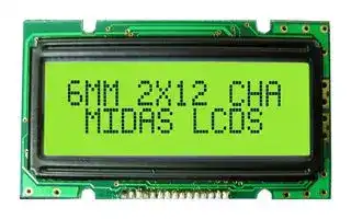
- Module Size: 55.7mm x 32mm
- Display Mode: Transflective
- Logic Voltage: 5V
- Product Range: -
- Character Size: 5.5mm
- Interface Type: Parallel
- LCD Display Type: STN
- Display Appearance: Black on Yellow / Green
- Backlighting Colour: Yellow
- Display Construction: COB
- Character Count x Line: 12 x 2
- Operating Temperature Max: 70°C
- Operating Temperature Min: -20°C
| Delivery and price | |
|---|---|
| Units per pack | 250 |
| Price | 6.88 € |
| Current stock | 10+ |
| Lead time | 30 days |
Sauls Wharf House Crittens Road Great Yarmouth Norfolk NR31 0AG

Telephone +44 (0)1493 602602 Email:sales@midasdisplays.com Email:tech@midasdisplays.com www.midasdisplays.com

|MC21205A6W1-SPTLY|MC21205A6W1-SPTLY|2 x 12|5mm Character Height|LCD Module|
|---|---|---|---|---|
|**Specification **|||||
|Version:    4|||Date:  25/02/2016||
|**Revision**|||||
|1<br>2<br>3<br>4|26/10/2012<br>17/10/2014<br>15/12/2014<br>25/02/2016||First Issue.<br>Remove IC information.<br>Correct Screw hole=R1.25.<br>Modify Precautions in use of LCD Modules & Static electricity test.||


|DisplayFeatures|DisplayFeatures|5V<br>Parallel<br>Transflective<br>5.50mm<br>STN<br>55.70 x 32.00 x 9.70mm|5V<br>Parallel<br>Transflective<br>5.50mm<br>STN<br>55.70 x 32.00 x 9.70mm|
|---|---|---|---|
|Character Count|2 x 12|||
|Appearance|Black on Yellow/Green|||
|Logic Voltage|5V|||
|Interface|Parallel|||
|Font Set|English/Japanese|||
|DisplayMode|Transflective|||
|Character Height|5.50mm|||
|LC Type|STN|||
|Module Size|55.70 x 32.00 x 9.70mm|||
|OperatingTemperature|-20°C ~ +70°C|||
|Construction|COB|COB<br>BoxQuantity|Weight/ Display|
|LED Backlight|Yellow|---|---|


* - For full design functionality, please use this specification in conjunction with the ST7066U specification. (Provided Separately)

|**Display Accessories**|**Display Accessories**|||**Optional Variants**|**Optional Variants**||
|---|---|---|---|---|---|---|
|**Part Number **|**Description **||**Fonts**||**Appearances**|**Voltage**|


Page 1 of 16

## **General Specification**

The Features is described as follow:

- Module dimension: 55.7 x 32.0 x 9.7 (max.) mm

- View area: 46.0 x 14.5 mm

- Active area: 37.85 x 11.7 mm

- Number of Characters: 12 characters x 2Lines

- Dot size: 0.45 x 0.60 mm

- Dot pitch: 0.55 x 0.70 mm

- Character size: 2.65 x 5.50 mm

- Character pitch: 3.20 x 6.20 mm

- LCD type: STN Positive, Yellow Green Transflective

- Duty: 1/16

- View direction: 6 o’clock

- Backlight Type: LED, Yellow Green

- IC:ST7066U

Page 2 of 16

## **Interface Pin Function**

|**Pin No. Symbol**|**Pin No. Symbol**|**Level**|**Description**|
|---|---|---|---|
|1|VSS|0V|Ground|
|2|VDD|5.0V|Supply Voltage for logic|
|3|VO|(Variable) Operating voltage for LCD|(Variable) Operating voltage for LCD|
|4|RS|H/L|H: DATA, L: Instruction code|
|5|R/W|H/L|H: Read   L: Write|
|6|E|H,H→L|Chip enable signal|
|7|DB0|H/L|Data bus line|
|8|DB1|H/L|Data bus line|
|9|DB2|H/L|Data bus line|
|10|DB3|H/L|Data bus line|
|11|DB4|H/L|Data bus line|
|12|DB5|H/L|Data bus line|
|13|DB6|H/L|Data bus line|
|14|DB7|H/L|Data bus line|
|15|A|-|LED+|


Page 3 of 16

## **Contour Drawing &Block Diagram**

**==> picture [402 x 189] intentionally omitted <==**

**----- Start of picture text -----**<br>
2.2 " 55.751.30.5 7 PINNO. SYMBOL<br>4.5 46.7 1 Vss<br>4.85 46.0(VA) 9.7Max 2 Vdd<br>8.93 37.85(AA) 5.1 3 Vo<br>4 RS<br>1 ! ! ! : | i]<br>A| 5 R/W<br>6 E<br>i — 7 DB0<br>8 DB1<br>9 DB2<br>! ' - 10 DB3<br>'<br>11 DB4<br>'<br>i 1 15 ! 1 12 DB5<br>1.0 13 DB6<br>4-R1.25 r 18.96 ia a) 17.78 i 15- 0.7PTH —_ 1.6 14 DB7<br>eli 15- ¢ 1.0PAD LED B/L 15 A<br>12.25 31.2<br>3.65 7.25 8.75 10.15 1.0<br>0.5<br>24.7 17.5 30.0<br>32.0 14.5(VA) 11.7(AA)<br>1.5<br>**----- End of picture text -----**<br>


**==> picture [398 x 302] intentionally omitted <==**

**----- Start of picture text -----**<br>
3.20<br>2.65<br>=<br>0.55<br>0.45<br>or 14 | lr Dd The non-specified tolerance of dimension is 0.3mm.<br>t l e! |<br>'<br>'<br>DOT SIZE<br>SCALE 5/1<br>RS Com1~16<br>R/W Controller/Com Driver<br>MPU<br>EDB0~DB7 ST7066Uor 12X2 LCD<br>Equivalent<br>68 series<br>Seg1~40<br>Vdd<br>Seg41~60<br>VR Vo D Seg Driver<br>10K~20K Vss<br>M<br>CL1<br>External contrast adjustment. CL2<br>Vdd,Vss,V1~V5<br>0.70 0.60<br>5.50<br>6.20<br>Bias and Power Circuit<br>**----- End of picture text -----**<br>


Character located 1 2 3 4 5 6 7 8 9 10 11 12 DDRAM address 00 01 02 03 04 05 06 07 08 09 0A 0B DDRAM address 40 41 42 43 44 45 46 47 48 49 4A 4B

Page 4 of 16

## **Character Generator ROM Pattern**

## Table.2

|Table.2|||||
|---|---|---|---|---|
|4 bit<br>Lower<br>4 bit<br>Upper|CG<br>RAM<br>LLLL|LLHH<br>LLHL<br>LLLH<br>LHLL|LHHH<br>LHLH<br>LHHL<br>HLLL|HLLH<br>HLHL HLHH<br>HHLH<br>HHLL|
|LLLL|RAM<br>( 1 )||||
|LLLH|( 2 )||||
|LLHL|( 3 )||||
|LLHH|( 4 )||||
|LHLL|( 5 )||||
|LHLH|( 6 )||||
|LHHL|( 7 )||||
|LHHH|( 8 )||||
|HLLL|( 1 )||||
|HLHL<br>HLLH|( 2 )||||
|HLHL|( 3 )||||
|HLHH|( 4 )||||
|HHLL|( 5 )||||
|HHLH|( 6 )||||
|HHHL|( 7 )||||
|HHHH|( 8 )||||


Page 5 of 16

## **Optical Characteristics**

|**Item**|**Symbol**|**Condition**|**Min**|**Typ**|**Max**|**Unit**|
|---|---|---|---|---|---|---|
|View Angle|θ|CR≧2|0|-|20|ψ= 180°|
||θ|CR≧2|0|-|40|ψ= 0°|
||θ|CR≧2|0|-|30|ψ= 90°|
||θ|CR≧2|0|-|30|ψ= 270°|
|Contrast Ratio|CR|-|-|3|-|-|
|Response Time|T rise|-|-|150|200|ms|
||T fall|-|-|150|200|ms|


**==> picture [492 x 189] intentionally omitted <==**

**----- Start of picture text -----**<br>
Definition of Operation Voltage (Vop) Definition of Response Time ( Tr , Tf )<br>Non-selected Non-selected<br>Condition Condition<br>Intensity Selected Wave — — S elected Condition p one<br>100 % _ Non-selected Wave Intensity r<br>!<br>1 1<br>10%<br>rY<br>Cr Max<br>Cr = Lon / Loff 90%<br>100%<br>\<br>' !<br>Vop<br>Driving Voltage(V) — T r — = T f — _<br>[positive type] 【 Positive type 】<br>**----- End of picture text -----**<br>


## **Conditions :**

Operating Voltage : Vop Viewing Angle(θ , φ) : 0° , 0° Frame Frequency : 64 HZ Driving Waveform : 1/N duty , 1/a bias

## **Definition of viewing angle(CR** ≧ **2)**

**==> picture [257 x 88] intentionally omitted <==**

**----- Start of picture text -----**<br>
θ b<br>θ f φ = 180 °<br>θ l<br>θ r<br>φ = 270 ° φ = 90 °<br>**----- End of picture text -----**<br>


**==> picture [25 x 9] intentionally omitted <==**

**----- Start of picture text -----**<br>
φ = 0 °<br>**----- End of picture text -----**<br>


Page 6 of 16

|**Absolute Maximum Ratings**|**Absolute Maximum Ratings**|**Absolute Maximum Ratings**|||||
|---|---|---|---|---|---|---|
|**Item**<br>**Symbol**<br>**Min**<br>**Typ**<br>**Max**<br>**Unit**<br>Operating Temperature<br>TOP<br>-20<br>-<br>+70<br>℃<br>Storage Temperature<br>TST<br>-30<br>-<br>+80<br>℃<br>Input Voltage<br>VI<br>VSS<br>-<br>VDD<br>V<br>Supply Voltage For Logic<br>VDD-VSS<br>-0.3<br>-<br>7<br>V<br>Supply Voltage For LCD<br>VDD-Vo<br>-0.3<br>-<br>13<br>V<br>~~=e~~|||||||
|**Electrical Characteristics**|||||||
|**Item**||**Symbol**<br>**Condition**|**Min**|**Typ**|**Max**|**Unit**|
|Supply Voltage For|||||||
|||VDD-VSS<br>-|4.5|5.0|5.5|V|
|Logic|||||||
|||Ta=-20℃|-|-|5.7|V|
|Supply Voltage For LCD||VDD-V0<br>Ta=25℃|4.1|4.2|4.3|V|
|* Note|||||||
|||Ta=70℃|3.5|-|-|V|
|Input High Volt.||VIH<br>-|0.7 VDD|-|VDD|V|
|Input Low Volt.||VIL<br>-|VSS|-|0.6|V|
|Output High Volt.||VOH<br>-|3.9|-|VDD|V|
|Output Low Volt.||VOL<br>-|0|-|0.4|V|
|Supply Current||IDD<br>VDD=5.0V|-|1.2|-|mA|


Note: Please design the VOP adjustment circuit on customer's main board

**==> picture [113 x 45] intentionally omitted <==**

**----- Start of picture text -----**<br>
Vdd<br>LCM<br>Vo<br>VR<br>10K~20K Module<br>VSS<br>**----- End of picture text -----**<br>


Page 7 of 16

## **Backlight Information**

## **Specification**

|**Specification**|||||||
|---|---|---|---|---|---|---|
|**PARAMETER**|**SYMBOL MIN**|**SYMBOL MIN**|**TYP**|**MAX**|**UNIT**|**TEST** **CONDITION**|
|**Supply Current ILED**|**Supply Current ILED**|**32**|**40**|**48**|**mA**|**V=4.2V**|
|**Supply Voltage V**|**Supply Voltage V**|**4.0**|**4.2**|**4.7**|**V**|-|
|**Reverse Voltage VR**|**Reverse Voltage VR**|-|-|**5**|**V**|-|
|**Luminance**<br>**(Without LCD)**|**IV**|**48**|**60**|-|**CD/M2 ILED=40mA**|**ILED=40mA**|
|**Wave Length**|**λp**|**565**|**569**|**575**|**nm**|**ILED=40mA**|
|**Life Time**|-|-|**100000**|-|**Hr.**|**ILED=40 mA**<br>**25℃,50-60%RH**|
|**Color**|**Yellow Green**||||||


**Note: The LED of B/L is drive by current only, drive voltage is for reference only. drive voltage can make driving current under safety area (current between minimum and maximum).**

## Drive from pin15,pin1

**==> picture [170 x 67] intentionally omitted <==**

**----- Start of picture text -----**<br>
R R<br>pin15 A<br>B/L<br>K<br>pin1<br>LCM<br>**----- End of picture text -----**<br>


Page 8 of 16

## **Reliability**

## **Content of Reliability Test (Wide temperature, -20** ℃ **~70** ℃ **)**

|**Content of Reliability Test (Wide temperature, -20**℃**~70**℃**)**|**Content of Reliability Test (Wide temperature, -20**℃**~70**℃**)**|**Content of Reliability Test (Wide temperature, -20**℃**~70**℃**)**|**Content of Reliability Test (Wide temperature, -20**℃**~70**℃**)**|
|---|---|---|---|
|**Environmental Test**||||
|**Test Item **|**Content of Test**|**Test Condition **|**Note**|
|High Temperature<br>storage|Endurance test applying the high storage temperature<br>foralong time.|80℃<br>200hrs|2|
|Low Temperature<br>storage|Endurance test applying the low storage temperature<br>foralong time.|-30℃<br>200hrs|1,2|
|High Temperature<br>Operation|Endurance test applying the electric stress (Voltage &<br>Current) and the thermal stress to the element for a<br>long time.|70℃<br>200hrs|——|
|Low Temperature<br>Operation|Endurance test applying the electric stress under low<br>temperatureforalong time.|-20℃<br>200hrs|1|
|High Temperature/<br>Humidity storage|The module should be allowed to stand at<br>60℃,90%RH max<br>For 96hrs under no-load condition excluding the<br>polarizer,<br>Thentakingit out and dryingit atnormaltemperature.|60℃,90%RH<br>96hrs|1,2|
|Thermal shock<br>resistance|The sample should be allowed stand the following 10<br>cycles of operation<br>-20℃25℃70℃<br>30min   5min    30min<br>1cycle|-20℃/70℃<br>10 cycles|——|
|Vibration test|Endurance test applying the vibration during<br>transportation and using.|Total fixed<br>amplitude : 1.5mm<br>Vibration Frequency :<br>10~55Hz<br>One cycle 60<br>seconds to 3<br>directions of X,Y,Z for<br>Each 15minutes|directions of X,Y,Z for<br>3|
|Static electricity test|Endurance test applying the electric stress to the<br>terminal.|VS=±600V(contact),<br>±800v(air),<br>RS=330Ω<br>CS=150pF<br>10 times|——|


**Note1: No dew condensation to be observed. Note2: The function test shall be conducted after 4 hours storage at the normal Temperature and humidity after remove from the test chamber. Note3: The packing have to including into the vibration testing.**

Page 9 of 16

## **Inspection specification**

|NO|Item|Criterion|AQL|
|---|---|---|---|
|01|Electrical<br>Testing|1.1 Missing vertical, horizontal segment, segment contrast<br>defect.<br>1.2 Missing character , dot or icon.<br>1.3 Display malfunction.<br>1.4 No function or no display.<br>1.5 Current consumption exceeds product specifications.<br>1.6 LCD viewing angle defect.<br>1.7 Mixed product types.<br>1.8 Contrast defect.|0.65|
|02|Black or white<br>spots on LCD<br>(display only)|2.1 White and black spots on display≦0.25mm, no more than<br>three white or black spots present.<br>2.2 Densely spaced: No more than two spots or lines within<br>3mm|2.5|
|03|LCD black<br>spots, white<br>spots,<br>contamination<br>(non-display)<br>~~E~~|3.1 Round type : As following drawing<br>Φ=( x + y ) / 2<br>SIZE<br>Acceptable Q TY<br>Φ≦0.10<br>Accept no dense<br>0.10<Φ≦0.20<br>2<br>0.20<Φ≦0.25<br>1<br>0.25<Φ<br>0<br>pi<br>v~~a~~<br>~~ESS~~|2.5<br>~~a~~<br>~~SS~~|
|||3.2 Line type : (As following drawing)<br>Length<br>Width<br>Acceptable Q TY<br>---<br>W≦0.02<br>Accept no dense<br>L≦3.0<br>0.02<W≦0.03<br>2<br>L≦2.5<br>0.03<W≦0.05<br>---<br>0.05<W<br>As round type<br>~~ESS~~|2.5<br>~~SS~~|
|04|Polarizer<br>bubbles<br>~~E~~|If bubbles are visible,<br>judge using black spot<br>specifications, not easy<br>to find, must check in<br>specify direction.<br>Size Φ<br>Acceptable Q TY<br>Φ≦0.20<br>Accept no dense<br>0.20<Φ≦0.50<br>3<br>0.50<Φ≦1.00<br>2<br>1.00<Φ<br>0<br>Total Q TY<br>3<br>~~ESS~~|2.5<br>~~SS~~|


Page 10 of 16

|NO<br>~~aa~~|Item<br>~~aa~~|Criterion<br>~~aa~~|AQL|
|---|---|---|---|
|05<br>~~a~~|Scratches<br>~~a~~|Follow NO.3 LCD black spots, white spots, contamination||
|06<br>~~a~~|Chipped<br>glass<br>~~a~~|Symbols Define:<br>x: Chip length      y: Chip width     z: Chip thickness<br>k: Seal width       t: Glass thickness  a: LCD side length<br>L: Electrode pad length:<br>6.1 General glass chip :<br>6.1.1 Chip on panel surface and crack between panels:<br>z: Chip thickness<br>y: Chip width<br>x: Chip length<br>Z≦1/2t<br>Not over viewing<br>area<br>x≦1/8a<br>1/2t<z≦2t<br>Not exceed 1/3k<br>x≦1/8a<br>☉If there are 2 or more chips, x is total length of each chip.<br>6.1.2 Corner crack:<br>z: Chip thickness<br>y: Chip width<br>x: Chip length<br>Z≦1/2t<br>Not over viewing<br>area<br>x≦1/8a<br>1/2t<z≦2t<br>Not exceed 1/3k<br>x≦1/8a<br>☉If there are 2 or more chips, x is the total length of each chip.|2.5|


Page 11 of 16

**==> picture [490 x 617] intentionally omitted <==**

**----- Start of picture text -----**<br>
NO  Item  Criterion<br>AQL<br>ee<br>Symbols :<br>x: Chip length      y: Chip width     z: Chip thickness<br>k: Seal width       t: Glass thickness  a: LCD side length<br>L: Electrode pad length<br>6.2 Protrusion over terminal :<br>6.2.1 Chip on electrode pad :<br>ES<br>y: Chip width  x: Chip length  z: Chip thickness<br>y ≦ 0.5mm  x ≦ 1/8a  0  <  z  ≦  t<br>6.2.2 Non-conductive portion:<br>L L<br>Glass<br>06  2.5<br>crack<br>y: Chip width  x: Chip length  z: Chip thickness<br>y ≦  L  x ≦ 1/8a  0  <  z  ≦  t<br>☉ If the chipped area touches the ITO terminal, over 2/3 of the ITO<br>must remain and be inspected according to electrode terminal<br>specifications.<br>☉ If the product will be heat sealed by the customer, the alignment<br>mark not be damaged.<br>6.2.3 Substrate protuberance and internal crack.<br>X<br>y: width  x: length<br>=.<br>y ≦ 1/3L  x  ≦  a<br>**----- End of picture text -----**<br>


Page 12 of 16

|NO|Item|Criterion|AQL|
|---|---|---|---|
|07|Cracked glass The LCD with extensive crack is not acceptable.|Cracked glass The LCD with extensive crack is not acceptable.|2.5|
|08|Backlight<br>elements|8.1 Illumination source flickers when lit.<br>8.2 Spots or scratched that appear when lit must be judged.<br>Using LCD spot, lines and contamination standards.<br>8.3 Backlight doesn’t light or color wrong.|0.65<br>2.5<br>0.65|
|09|Bezel|9.1 Bezel may not have rust, be deformed or have fingerprints,<br>stains or other contamination.<br>9.2 Bezel must comply with job specifications.|2.5<br>0.65|
|10|PCB、COB|10.1 COB seal may not have pinholes larger than 0.2mm or<br>contamination.<br>10.2 COB seal surface may not have pinholes through to the<br>IC.<br>10.3 The height of the COB should not exceed the height<br>indicated in the assembly diagram.<br>10.4 There may not be more than 2mm of sealant outside the<br>seal area on the PCB. And there should be no more than<br>three places.<br>10.5 No oxidation or contamination PCB terminals.<br>10.6 Parts on PCB must be the same as on the production<br>characteristic chart. There should be no wrong parts,<br>missing parts or excess parts.<br>10.7 The jumper on the PCB should conform to the product<br>characteristic chart.<br>10.8 If solder gets on bezel tab pads, LED pad, zebra pad or<br>screw hold pad, make sure it is smoothed down.<br>10.9 The Scraping testing standard for Copper Coating of PCB<br>~~**Y**~~<br>~~**X**~~<br>X * Y<=2mm2|2.5<br>2.5<br>0.65<br>2.5<br>2.5<br>0.65<br>0.65<br>2.5<br>2.5|
|11|Soldering|11.1 No un-melted solder paste may be present on the PCB.<br>11.2 No cold solder joints, missing solder connections,<br>oxidation or icicle.<br>11.3 No residue or solder balls on PCB.<br>11.4 No short circuits in components on PCB.|2.5<br>2.5<br>2.5<br>0.65|


Page 13 of 16

|NO|Item|Criterion|AQL|
|---|---|---|---|
|12|General<br>appearance|12.1 No oxidation, contamination, curves or, bends on interface<br>Pin (OLB) of TCP.<br>12.2 No cracks on interface pin (OLB) of TCP.<br>12.3 No contamination, solder residue or solder balls on product.<br>12.4 The IC on the TCP may not be damaged, circuits.<br>12.5 The uppermost edge of the protective strip on the interface<br>pin must be present or look as if it cause the interface pin to<br>sever.<br>12.6 The residual rosin or tin oil of soldering (component or chip<br>component) is not burned into brown or black color.<br>12.7 Sealant on top of the ITO circuit has not hardened.<br>12.8 Pin type must match type in specification sheet.<br>12.9 LCD pin loose or missing pins.<br>12.10 Product packaging must the same as specified on<br>packaging specification sheet.<br>12.11 Product dimension and structure must conform to product<br>specification sheet.<br>12.12 Visual defect outside of VA is not considered to be<br>rejection.|2.5<br>0.65<br>2.5<br>2.5<br>2.5<br>2.5<br>2.5<br>0.65<br>0.65<br>0.65<br>0.65|


Page 14 of 16

## **Precautions in use of LCD Modules**

- (1) Avoid applying excessive shocks to the module or making any alterations or modifications to it.

- (2) Don’t make extra holes on the printed circuit board, modify its shape or change the components of LCD module.

- (3) Don’t disassemble the LCM.

- (4) Don’t operate it above the absolute maximum rating.

- (5) Don’t drop, bend or twist LCM.

- (6) Soldering: only to the I/O terminals.

- (7) Storage: please storage in anti-static electricity container and clean environment.

- (8) MIDAS have the right to change the passive components, including R3,R6 & backlight adjust resistors. (Resistors,capacitors and other passive components will have different appearance and color caused by the different supplier.)

- (9) MIDAS have the right to change the PCB Rev. (In order to satisfy the supplying stability, management optimization and the best product performance...etc, under the premise of not affecting the electrical characteristics and external dimensions, MIDAS have the right to modify the version.)

- (10) To ensure the stability of the display screen, please apply screen saver after showing 30 mins of fixed display content.

Page 15 of 16

## **Material List of Components for RoHs**

1. MIDAS hereby declares that all of or part of products (with the mark

   - “#”in code), including, but not limited to, the LCM, accessories or packages, manufactured and/or delivered to your company (including your subsidiaries and affiliated company) directly or indirectly by our company (including our subsidiaries or affiliated companies) do not intentionally contain any of the substances listed in all applicable EU directives and regulations, including the following substances.

Exhibit A : The Harmful Material List

|Material|(Cd)|(Pb)|(Hg)|(Cr6+)|PBBs|PBDEs|
|---|---|---|---|---|---|---|
|Limited<br>Value|100<br>ppm|1000<br>ppm|1000<br>ppm|1000<br>ppm|1000<br>ppm|1000<br>ppm|
|Above limited value is set upaccordingto RoHS.|||||||


- 2.Process for RoHS requirement : (only for RoHS inspection)

   - (1) Use the Sn/Ag/Cu soldering surface ; the surface of Pb-free solder is rougher than we used before.

   - (2) Heat-resistance temp. :

Reflow : 250 ℃ ,30 seconds Max. ;

Connector soldering wave or hand soldering : 320 ℃ , 10 seconds max.

- (3) Temp. curve of reflow, max. Temp. : 235±5 ℃;

Recommended customer’s soldering temp. of connector : 280 ℃ , 3 seconds.

## **Recommendable Storage**

1. Place the panel or module in the temperature 25°C±5°C and the humidity below 65% RH

2. Do not place the module near organics solvents or corrosive gases.

3. Do not crush, shake, or jolt the module.

Page 16 of 16
Updated at April 26, 2026
Midas Displays is a recognized specialist in the electronic display industry, dedicated to providing high-quality visual solutions tailored to a wide range of applications. Backed by a UK-based, in-house team of engineers, the company is known for its extensive technical knowledge and commitment to delivering fast, reliable service. This expertise ensures that designers and manufacturers receive best-in-class support when integrating displays into their projects. The core of the Midas Displays portfolio features an extensive selection of Liquid Crystal Displays (LCD). Ranging from standard character and graphic modules to advanced configurations, these LCD displays are engineered for exceptional clarity and durability. Designed to meet the rigorous demands of various industries, they provide reliable performance for both industrial and commercial applications requiring robust and cost-effective visual output. Complementing their primary LCD offerings, Midas Displays also provides a versatile range of Organic Light Emitting Diode (OLED) displays. These advanced modules deliver high-contrast, energy-efficient viewing solutions ideal for modern, compact electronic designs. To ensure seamless integration across all display types, the company supports its core products with a variety of complementary accessories, including touch screens, interconnects, and evaluation kits.
About Novapart
Novapart is a B2B electronic component broker specialising in stock shortages and cost reduction. We source hard-to-find parts and identify compliant alternatives across a catalogue of 410,000+ components from 500+ manufacturers.
Learn more →Stock Shortage Specialist
When a component is unavailable, discontinued or has an unacceptable lead time, we tap into our network of vetted European and Asian distributors to source what you need — without compromising on quality or traceability.
Request a quote →Compliant Alternatives
We identify pin-to-pin, electrically equivalent substitutes that meet the same certifications (RoHS, AEC-Q100, REACH) as your original specification — validated against datasheets, not just part numbers. Often at a lower cost.
BOM Analysis service →