


MAXM38643AEMB+
DC/DC POL Converter, Adjustable, Boost, 1.8 V to 5.5 V in, 0.7 V to 3.3 V /0.6 A out, eMGA-10
- Manufacturer: ANALOG DEVICES
- Product type: DC / DC Non Isolated Board Mount Converters - Adjustable Output
- Available until stocks are exhausted
- MSL: MSL 3 - 168 hours
- SVHC: No SVHC (21-Jan-2025)
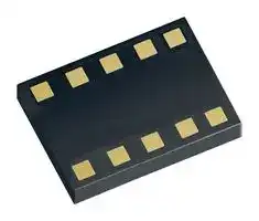
- Depth: 2.1mm
- Width: 2.6mm
- Height: -
- Topology: Buck (Step Down)
- No. of Pins: 10Pins
- Product Range: MAXM38643 Series
- No. of Outputs: 1 Output
- Output Current: 600mA
- Output Power Max: -
- Input Voltage Max: 5.5V
- Input Voltage Min: 1.8V
- Output Current Max: 600mA
- Output Voltage Max: 3.3V
- Output Voltage Min: 700mV
- Input Voltage DC Max: 5.5V
- Input Voltage DC Min: 1.8V
- DC / DC Converter Type: eMGA-10, Module
- DC / DC Converter IC Case: eMGA
- Operating Temperature Max: 85°C
- Power Supply Applications: ITE
- DC / DC Converter Output Type: Adjustable
| Delivery and price | |
|---|---|
| Units per pack | 500 |
| Price | 2.32 € |
| Current stock | 10+ |
| Lead time | 30 days |
_Evaluation Kit Design Tools Support Available Resources and Models_

_Click here to ask an associate for production status of specific part numbers._

**MAXM38643**

**==> picture [176 x 34] intentionally omitted <==**

## **Tiny, 1.8V to 5.5V Input, 330nA IQ, 600mA nanoPower Buck Module**

## **Product Highlights**

- Extends Battery Life

   - 330nA Ultra-Low Quiescent Supply Current

   - 1nA Shutdown Current

   - 96% Peak Efficiency and over 88% at 10µA

- Easy to Use – Addresses Popular Operations • 1.8V to 5.5V Input Range

   - Single Resistor-Adjustable VOUT from 0.7V to 3.3V

   - Factory-Preprogrammed VOUT from 0.5V to 5V

   - ±1.75% Output Voltage Accuracy

   - Up to 600mA Load Current Capability

- Protects System in Multiple Use Cases

   - Reverse-Current Blocking in Shutdown

## **Simplified Application Diagram**

**==> picture [203 x 142] intentionally omitted <==**

**----- Start of picture text -----**<br>
LX<br> INPUT IN OUT OUTPUT<br>IN OUT<br>CIN OUTS COUT<br>22µF 2 x 22µF<br>MAXM38643<br>EN RSEL<br>RSEL<br>GND GND<br>**----- End of picture text -----**<br>


   - Active Discharge Feature

- Reduces Size and Increases Reliability

   - -40°C to +85°C Temperature Range

   - 2.1mm x 2.6mm, 10-Lead eMGA Package

## **Key Applications**

- Portable Space-Constrained Products

- Wearables

- Hearables

- Ultra-Low-Power IoT, NB IoT

- Bluetooth[®] LE Devices

- Single Li+ and Coin Cell Battery Products

- Wired, Wireless Products

_Bluetooth is a registered trademark of Bluetooth SIG, Inc._

## **Pin Description**

**==> picture [193 x 219] intentionally omitted <==**

**----- Start of picture text -----**<br>
TOP VIEW<br>OUT 1 10 EN<br>OUT 2 9 IN<br>OUTS 3 MAXM38643 8 IN<br>RSEL 4 7 GND<br>LX 5 6 GND<br>**----- End of picture text -----**<br>


_**Ordering Information appears at end of data sheet.**_

_19-101138; Rev 0; 7/21_

MAXM38643

## Tiny, 1.8V to 5.5V Input, 330nA IQ, 600mA nanoPower Buck Module

|**Absolute Maximum Ratings**||
|---|---|
|IN, EN, RSEL, OUT, OUTS to GND ...................... -0.3V to +6V|Operating Temperature Range ......................... -40°C to +85°C|
|LX to GND ................................................... -0.3V to VIN+ 0.3V|Maximum Junction Temperature ................................... +150°C|
|Continuous Power Dissipation (TA= +70°C) .............................|Storage Temperature Range .......................... -65°C to +150°C|
|eMGA Package (derate 9.72 mW/°C above 70°C) .. 777.91mW|Lead Temperature (soldering, 10 seconds) .................. +300°C|
||Soldering Temperature (reflow) ..................................... +260°C|


**Note 1:** LX pin has internal clamps to GND and IN. These diodes may be forward biased during switching transitions.

_Stresses beyond those listed under “Absolute Maximum Ratings” may cause permanent damage to the device. These are stress ratings only, and functional operation of the device at these or any other conditions beyond those indicated in the operational sections of the specifications is not implied. Exposure to absolute maximum rating conditions for extended periods may affect device reliability._

## **Package Information**

## **10 eMGA**

|**Package Information**<br>**10 eMGA**||
|---|---|
|Package Code|M102A2+2|
|Outline Number|_21-100245*_|
|Land Pattern Number|_90-100084*_|
|**Thermal Resistance, Four-Layer Board:**||
|Junction to Ambient(θJA)|102.84°C/W|
|Junction to Case(θJC)|15.04°C/W|


*For the latest package outline information and land patterns (footprints), go to www.maximintegrated.com/packages _._ Note that a “+”, “#”, or “-” in the package code indicates RoHS status only. Package drawings may show a different suffix character, but the drawing pertains to the package regardless of RoHS status.

Package thermal resistances were obtained using the method described in JEDEC specification JESD51-7, using a four-layer board. For detailed information on package thermal considerations, refer to _www.maximintegrated.com/thermal-tutorial_ .

## **Electrical Characteristics**

(VIN = 3.3V, VOUT = VOUTS = 1.8V, TA = -40°C to +85°C, CIN = 1 x 22µF, COUT = 2 x 22µF, unless otherwise specified. See _Note 2_ .)

|**PARAMETER**|**SYMBOL**|**CONDITIONS**|**CONDITIONS**|**MIN**<br>**TYP**<br>**MAX**|**UNITS**|
|---|---|---|---|---|---|
|Input Voltage Range|VIN|Guaranteed by input undervoltage<br>lockout and output accuracy||1.8<br>5.5|V|
|Input Undervoltage<br>Lockout|VUVLO|RSEL> 60kΩ|VINrising|1.759<br>1.8|V|
||||VINfalling|1.713||
||||Hysteresis|50|mV|
|||RSEL< 60kΩ|VINrising|2.624<br>2.7|V|
||||VINfalling|2.499||
||||Hysteresis|125|mV|
|Output Voltage Range|VOUT|Guaranteed by output accuracy(_Table 1_)||0.7<br>3.3|V|
|Maximum Output<br>Current|IOUT|VIN= 3.6V||600|mA|
|Output Accuracy|VOUT_ACC|VOUTSfalling, when LX begins switching<br>above 500kHz, VOUT= VOUTS= 0.7V to<br>3.3V, VIN= 1.8V to 5.5V, VIN> VOUTS+<br>0.3V(_Note 3_)||-1.75<br>+1.75|%|
|DC Line Regulation|VOUT_LREG|VOUT = 1.8V, VIN= 2.0V to 5.5V,<br>IOUT from 10mA to 500mA||±1.5|%|
|Efficiency|η|VIN= 3.6V, VOUT = 1.8V, IOUT= 100μA||92|%|
|||VIN= 3.6V, VOUT = 1.8V, IOUT= 100mA||94||
|||VIN= 5.0V, VOUT = 1.8V, IOUT= 100μA||90||


www.maximintegrated.com

Maxim Integrated | 2

MAXM38643

## Tiny, 1.8V to 5.5V Input, 330nA IQ, 600mA nanoPower Buck Module

(VIN = 3.3V, VOUT = VOUTS = 1.8V, TA = -40°C to +85°C, CIN = 1 x 22µF, COUT = 2 x 22µF, unless otherwise specified. See _Note 2_ .)

|**PARAMETER**|**SYMBOL**|**CONDITIONS**|**MIN**<br>**TYP**<br>**MAX**|**UNITS**|
|---|---|---|---|---|
|||VIN= 5.0V, VOUT = 1.8V, IOUT= 100mA|92||
|||VIN= 4.2V, VOUT = 3.3V, IOUT= 100μA|94||
|||VIN= 4.2V, VOUT = 3.3V, IOUT= 200mA|96||
|Quiescent Supply<br>Current into IN|IQ_IN|VEN= VIN, not switching VOUTS= 104%<br>of target voltage, VOUTS_TARGET= 2.5V,<br>TA= +25°C|330<br>660|nA|
|Quiescent Supply<br>current into OUT|IQ_OUT|VEN= VIN, not switching VOUTS= 104%<br>of target voltage,TA= +25°C|5|nA|
|Shutdown Current into<br>IN|IIN_SD|VEN= 0V, VOUT= VOUTS= VLX= 0V,<br>TA= +25°C|0.001<br>0.1|µA|
|Soft-Start Time|tSS|No load|250|µs|
|Inductor Peak Current<br>Limit|IPEAK_LX|VINfrom 2.0V to 5.5V|800<br>1000<br>1200|mA|
|Inductor Current Zero<br>CrossingThreshold|IZX_LX|VOUT= VOUTS= 1.2V, percent of<br>IPEAK_LX|5|%|
|High-Side RDSON|HS_ RDSON|VIN= 3.3V|95<br>150|mΩ|
|Low-Side RDSON|LS_ RDSON|VIN= 3.3V|50<br>90|mΩ|
|Enable Voltage<br>Threshold|VIH|VENrising|0.841<br>1.2|V|
||VIL|VENfalling|0.4<br>0.701||
|Enable Input Leakage<br>Current|ILK_EN|VEN= 5.5V, TA= +25°C|0.004<br>1|µA|
|Active Discharge<br>Resistance|ROUT_DIS|VEN= 0V|50<br>85.4<br>200|Ω|
|Required Select<br>Resistor Accuracy|RSEL|Use the nearest ±1% resistor from _Table_<br>_1_|-1<br>+1|%|
|Select Resistor<br>Detection Time|tRSEL|CRSEL< 2pF|360<br>600<br>1200|µs|
|Thermal Shutdown<br>Threshold|TSD|TArising when output turns OFF|165|°C|
|||TAfalling when output turns ON|150||


**Note 2:** Limits over the specified operating temperature and supply voltage range are guaranteed by design and characterization, and production tested at room temperature only.

**Note 3:** Output accuracy in low-power mode (LPM) and does not include load, line, or ripple.

www.maximintegrated.com

Maxim Integrated | 3

Tiny, 1.8V to 5.5V Input, 330nA IQ, 600mA nanoPower Buck Module

MAXM38643

## **Typical Application Circuit**

**==> picture [247 x 172] intentionally omitted <==**

**----- Start of picture text -----**<br>
LX<br> INPUT OUTPUT<br>1.8V TO 5.5V IN OUT 1V<br>IN OUT<br>CIN OUTS COUT<br>22µF<br>2 x 22µF<br>MAXM38643<br>EN RSEL<br>191k<br>GND GND<br>**----- End of picture text -----**<br>


## **Typical Operating Characteristics**

(MAXM38643AEMB+T, VIN = 3.6V, VOUT = 1.8V, L = 1.5µH (integrated), CIN = 1 x 22µF, COUT = 2 x 22µF, TA = +25°C unless otherwise specified.)

**==> picture [498 x 157] intentionally omitted <==**

www.maximintegrated.com

Maxim Integrated | 4

MAXM38643

## Tiny, 1.8V to 5.5V Input, 330nA IQ, 600mA nanoPower Buck Module

(MAXM38643AEMB+T, VIN = 3.6V, VOUT = 1.8V, L = 1.5µH (integrated), CIN = 1 x 22µF, COUT = 2 x 22µF, TA = +25°C unless otherwise specified.)

www.maximintegrated.com

Maxim Integrated | 5

MAXM38643

## Tiny, 1.8V to 5.5V Input, 330nA IQ, 600mA nanoPower Buck Module

(MAXM38643AEMB+T, VIN = 3.6V, VOUT = 1.8V, L = 1.5µH (integrated), CIN = 1 x 22µF, COUT = 2 x 22µF, TA = +25°C unless otherwise specified.)

- `

www.maximintegrated.com

Maxim Integrated | 6

Tiny, 1.8V to 5.5V Input, 330nA IQ, 600mA nanoPower Buck Module

MAXM38643

## **Pin Configuration**

**==> picture [222 x 251] intentionally omitted <==**

**----- Start of picture text -----**<br>
TOP VIEW<br>OUT 1 10 EN<br>OUT 2 9 IN<br>MAXM38643<br>OUTS 3 8 IN<br>RSEL 4 7 GND<br>LX 5 6 GND<br>**----- End of picture text -----**<br>


## **Pin Descriptions**

|**PIN**|**NAME**|**FUNCTION**|
|---|---|---|
|1, 2|OUT|Output Voltage Power Pins. Connect 2 x 22µF (2 in parallel, 22µF each) ceramic capacitors from OUT to<br>GND.|
|3|OUTS|Output Voltage Sense Pin. Connect to the point where accurate regulation (output capacitor) is required.|
|4|RSEL|Output Voltage Select Input. Connect a resistor from RSELto GND to program the output voltage and IN<br>undervoltage lockout threshold based on the values in _Table 1_.|
|5|LX|Switching Node Pin. Must be left floating; used by factory for testing only.|
|6, 7|GND|Ground Pins. Connect to the system ground.|
|8, 9|IN|Module Supply Input Pins. Connect a 22µF ceramic capacitor from IN to GND.|
|10|EN|Enable Input. Force this pin high to enable the buck module. Force this pin low to disable the part and<br>enter shutdown.|


www.maximintegrated.com

Maxim Integrated | 7

Tiny, 1.8V to 5.5V Input, 330nA IQ, 600mA nanoPower Buck Module

MAXM38643

## **Simplified Block Diagram**

**==> picture [456 x 313] intentionally omitted <==**

**----- Start of picture text -----**<br>
MAXM38643<br>INPUT IN<br>REVERSE<br>IN BLOCKING<br>LX<br>UVLO<br>CIN CURRENT SENSE<br>22µF EN<br>MODULATOR AND CONTROL 1.5µH OUT OUTPUT<br>VREF SHUTDOWNTHERMAL  OUT<br>COUT<br>2 x 22µF<br>OUTS<br>REFERENCE<br>FB<br>UVLO AND<br>RSEL OUTPUT<br>VOLTAGE<br>SELECTOR<br>RSEL<br>GND GND<br>ACTIVE DISCHARGE<br>**----- End of picture text -----**<br>


## **Detailed Description**

The MAXM38643 is an ultra-low-IQ (330nA) buck module that steps down input voltages in the range of 1.8V to 5.5V to a wide range of output voltages between 0.7V to 3.3V (using a single resistor at the RSEL pin). The output voltage is programmable upon startup using a single external resistor from the RSEL pin to GND. Factory-preprogrammed fixed output voltage versions from 0.5V to 5V are also available that do not use the RSEL pin to set the output voltage. In this case, the RSEL pin in the module is left floating.

The module offers robust performance features. To optimize efficiency and transient response across the load operation range, the module automatically switches between ultra-low-power mode (ULPM), low-power mode (LPM), and highpower mode (HPM) to better service the load, depending on the load current. The device overregulates in ULPM to improve efficiency and allow the output capacitor to handle the transient load currents. The device has 90% duty cycle limitation. An active discharge resistor pulls OUT to ground when the part is in shutdown.

## **Control Scheme**

The output voltage is regulated higher while in ULPM. This reduces switching frequency, thus significantly improving system efficiency. In addition, operating marginally above the regulation threshold, the device has an excellent transient response when a large load transient event occurs.

Each switching cycle begins by turning the high-side power FET on. The inductor current ramps up to the inductor peak current-limit level at which point the on-time is terminated. Subsequently, the synchronous power FET turns on, and the inductor current ramps down until it reaches zero, at which point the switching ceases. During this single switching cycle,

www.maximintegrated.com

Maxim Integrated | 8

MAXM38643

## Tiny, 1.8V to 5.5V Input, 330nA IQ, 600mA nanoPower Buck Module

a fixed amount of charge gets transferred to the output capacitor, thus increasing the output voltage. If the output voltage reaches the ULPM upper regulation threshold, the device will go into sleep mode to preserve energy. However, if one cycle is not enough for the output voltage to reach the upper threshold, as it may be the case at higher load levels, the device will burst switching pulses together every 10µs until the threshold is reached. The upper regulation threshold in ULPM is 2.7% (nominal) above the regulation target in LPM.

Once the output voltage exceeds the upper ULPM regulation level, the device will go into a sleep mode, consuming very low quiescent current. The load current slowly discharges the output capacitor, causing the output voltage to ramp down. The MAXM38643 wakes up to resume switching only when the output voltage falls below the upper regulation threshold. In ULPM, the device regulates output voltage while consuming only 330nA of quiescent current.

The MAXM38643 transitions to LPM once the load current is high enough that it forces the device to switch faster than every 10µs to maintain regulation.

Once in the LPM, the device regulates the output voltage to the lower regulation, which is the output voltage target level in LPM. Again, each switching cycle begins by turning the high-side power FET on. The inductor current ramps up to the inductor peak current limit level, at which point the on-time is terminated. Subsequently, the synchronous power FET turns on and the inductor current ramps down until the inductor current reaches zero. During this switching cycle, a quantity of charge gets transferred to the output capacitor, thus increasing the output voltage. The load current discharges the output capacitor to the lower regulation threshold, at which point a new switching cycle is initiated and the process repeats.

When the output current level rises to the levels where the inductor current ripple does not reach the zero-ampere level, the module transitions to high-power mode (HPM) or continuous-conduction mode (CCM). In this mode, the inductor current ripple is smaller than in ULPM and LPM to support higher load levels. This also assures a smooth transition between the modes.

**==> picture [465 x 280] intentionally omitted <==**

**----- Start of picture text -----**<br>
ULTRA-LOW-POWER MODE (ULPM) – LIGHT LOADS<br>VOUT<br>VOUT_TARGET + VOUT_HYSTERESIS<br>LOW-POWER MODE (LPM) – MEDIUM LOADS<br>HIGH-POWER MODE (HPM) – HEAVY LOADS<br>DCM DCM CCM<br>10µs<br>VOUT_TARGET<br>VOUT_TARGET - LOAD REG<br> IL<br>*LOAD<br>CURRENT<br>IN HPM * DEPENDS ON VIN, VOUT<br>IOUT<br>*LOAD   UP TO 600mA<br>CURRENT<br>*LOAD CURRENT IN ULPM<br>IN LPM<br>UP TO 40mA<br>UP TO 220mA<br>TIME<br>**----- End of picture text -----**<br>


_Figure 1. Mode Transitions_

www.maximintegrated.com

Maxim Integrated | 9

Tiny, 1.8V to 5.5V Input, 330nA IQ, 600mA nanoPower Buck Module

MAXM38643

## **Integrated Inductor**

A 1.5μH integrated inductor is used in the MAXM38643 buck module. The chosen inductor (Murata part# DFE201610E1R5M=P2), offers optimized stability across the device operation range.

## **Voltage Configuration**

The MAXM38643 includes an RSEL pin to configure the output voltage and input UVLO threshold on startup. Resistors with a tolerance of 1% (or better) should be chosen with the nominal values specified in _Table 1_ .

## **Table 1. MAXM38643A RSEL Selection Table**

|**TARGET OUTPUT VOLTAGE (V)**|**RSEL (kΩ)**|**INPUT UVLO THRESHOLD, RISING (V)**|
|---|---|---|
|2.5|OPEN|1.75|
|2.0|909|1.75|
|1.8|768|1.75|
|1.5|634|1.75|
|1.3|536|1.75|
|1.25|453|1.75|
|1.2|383|1.75|
|1.15|324|1.75|
|1.1|267|1.75|
|1.05|226|1.75|
|1.0|191|1.75|
|0.95|162|1.75|
|0.9|133|1.75|
|0.85|113|1.75|
|0.8|95.3|1.75|
|0.75|80.6|1.75|
|0.7|66.5|1.75|
|3.3|56.2|2.6|
|3.0|47.5|2.6|
|2.8|40.2|2.6|
|2.75|34|2.6|
|2.5|28|2.6|
|2.0|23.7|2.6|
|1.8|20|2.6|
|1.5|16.9|2.6|
|1.25|14|2.6|
|1.2|11.8|2.6|
|1.15|10|2.6|
|1.1|8.45|2.6|
|1.0|7.15|2.6|
|0.95|5.9|2.6|
|0.9|4.99|2.6|
|0.8|SHORT TO GND|2.6|


## **Fixed Output Voltage Versions – Factory Preprogrammed**

Note that MAXM38643 can also be ordered with a factory-preprogrammed fixed output voltage (no RSEL programming). In this configuration, the RSEL resistor is not required, and the RSEL pin shall be left floating. Contact a Maxim Integrated Representative for more information and availability for select preprogrammed VOUT.

## **Applications Information**

## **Input Capacitor**

The input capacitor (CIN) reduces the peak current drawn from battery or input power source and reduces the switching noise in the module. The impedance of CIN at the switching frequency should be very low. Ceramic capacitors are

www.maximintegrated.com

Maxim Integrated | 10

MAXM38643

## Tiny, 1.8V to 5.5V Input, 330nA IQ, 600mA nanoPower Buck Module

recommended for their small size and low ESR. For most applications, use a 22µF ceramic capacitor with X5R or X7R temperature characteristics. When operating at a VIN close to the UVLO, more input capacitance may be required to keep the input voltage ripple from tripping the UVLO protection.

## **Output Capacitor**

The output capacitor (COUT) is required to keep the output voltage ripple small and to ensure loop stability. COUT must have low impedance at the switching frequency. Ceramic capacitors are recommended due to their small size and low ESR. Make sure the capacitor does not degrade its capacitance significantly over temperature and DC bias. Capacitors with X5R or X7R temperature characteristics typically perform well. It is recommended to have 30µF of effective capacitance at COUT.

## **Enabling Device**

The device has a dedicated EN pin. This pin can be driven by a digital signal. It is recommended that the digital signal enables the device after VIN crosses the UVLO threshold. If the enable feature is unused, short the EN pin to IN. Connect the EN pin to the IN pin or drive it to more than 0.85V nominal (VIH) for normal operation. When the EN pin goes below 0.7V nominal (VIL), the MAXM38643 enters shutdown mode where the output gets pulled to ground through an 85Ω active discharge circuit. In addition, the body diode of the high-side FET is biased so that it prohibits any reverse-current flow back to the input. The device consumes 1nA (IIN_SD) of current from IN while in shutdown mode.

The device is designed to be powered by fast VIN slew rates. In applications where EN is tied to IN and where VIN slew rates are slower than 5V/ms, users must delay enabling the device after VIN crosses the UVLO threshold. This can be done using a simple RC circuit, as shown in _Figure 2_ .

**==> picture [112 x 101] intentionally omitted <==**

**----- Start of picture text -----**<br>
IN<br>BAT54 REN<br>EN<br>CEN<br>**----- End of picture text -----**<br>


_Figure 2. Simple RC Circuit_

## **PCB Layout and Routing**

High switching frequencies and large peak currents make PCB layout a very important part of the buck converter design. Good design minimizes excessive electromagnetic interference (EMI) in the feedback path and voltage gradients in the ground plane to avoid instability and regulation errors. The input capacitor (CIN) should be placed as close as possible to the module IN and GND pins. Connect the input capacitor (CIN) and output capacitor (COUT) grounds together through a short, wide connection. Connect the module GND pins directly to the ground of CIN. The OUTS pin should be connected to the output capacitor, and this trace should be routed away from the main power path between CIN and COUT. Refer to the MAXM38643 evaluation kit for an example of a PCB layout and routing scheme.

## **Ordering Information**

|**PART NUMBER**|**TEMPERATURE**<br>**RANGE**|**PIN PACKAGE**|**FEATURES**|
|---|---|---|---|
|MAXM38643AEMB+T|-40°C to +85°C|10-lead eMGA package<br>(2.1mm x 2.6mm,0.5mmpitch)|0.7V to 3.3V resistor-selectable output<br>voltage usingRSEL pin|
|MAXM38643BEMB+T*|-40°C to +85°C|10-lead eMGA package<br>(2.1mm x 2.6mm,0.5mmpitch)|0.5V to 5V preprogrammed output<br>voltage|


_+ Denotes a lead (Pb)-free/RoHS-compliant package. T = tape-and-reel_

_*Contact factory/Maxim Sales Representative for availability._

www.maximintegrated.com

Maxim Integrated | 11

Tiny, 1.8V to 5.5V Input, 330nA IQ, 600mA nanoPower Buck Module

MAXM38643

## **Revision History**

|**Revision**|**History**|||
|---|---|---|---|
|**REVISION**<br>**NUMBER**|**REVISION**<br>**DATE**|**DESCRIPTION**|**PAGES**<br>**CHANGED**|
|0|7/21|Initial release|—|


For pricing, delivery, and ordering information, please visit Maxim Integrated’s online storefront at https://www.maximintegrated.com/en/storefront/storefront.html.

_Maxim Integrated cannot assume responsibility for use of any circuitry other than circuitry entirely embodied in a Maxim Integrated product. No circuit patent licenses are implied. Maxim Integrated reserves the right to change the circuitry and specifications without notice at any time. The parametric values (min and max limits) shown in the Electrical Characteristics table are guaranteed. Other parametric values quoted in this data sheet are provided for guidance._

© 2021 Maxim Integrated Products, Inc.

Maxim Integrated and the Maxim Integrated logo are trademarks of Maxim Integrated Products, Inc.
Updated at April 10, 2026
Since its inception in 1965, Analog Devices has established itself as a global leader in the design and manufacturing of high-performance analog, mixed-signal, and digital signal processing (DSP) integrated circuits. The company is renowned for solving complex engineering challenges by providing critical technologies that seamlessly convert real-world phenomena into precise electrical signals for the industrial, automotive, communications, and consumer markets. Within its extensive portfolio, Analog Devices provides highly reliable clock, timing, and frequency management solutions, featuring a comprehensive array of precision timers, oscillators, and pulse generators. Complementing this core lineup is a robust offering of driver and interface ICs, particularly high-performance I/O expanders that enable seamless connectivity and streamline complex electronic system architectures. Beyond these foundational integrated circuits, Analog Devices leads the industry in sensor innovation, delivering advanced MEMS accelerometers and integrated MEMS modules designed for exceptional precision in motion sensing. To support complete hardware designs, the company's specialized offerings also encompass discrete bipolar transistors, sub-2.4GHz RF transceivers, temperature-compensated oscillators, and dedicated power management components such as DC/DC converters and LED driver ICs.
About Novapart
Novapart is a B2B electronic component broker specialising in stock shortages and cost reduction. We source hard-to-find parts and identify compliant alternatives across a catalogue of 410,000+ components from 500+ manufacturers.
Learn more →Stock Shortage Specialist
When a component is unavailable, discontinued or has an unacceptable lead time, we tap into our network of vetted European and Asian distributors to source what you need — without compromising on quality or traceability.
Request a quote →Compliant Alternatives
We identify pin-to-pin, electrically equivalent substitutes that meet the same certifications (RoHS, AEC-Q100, REACH) as your original specification — validated against datasheets, not just part numbers. Often at a lower cost.
BOM Analysis service →