
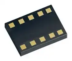


MAXM17906AMB+T
Non Isolated POL DC/DC Converter, Industrial, uSLIC-10, Module, 900 mV, 6.3 V, 300 mA
- Manufacturer: ANALOG DEVICES
- Product type: DC / DC Non Isolated Board Mount Converters - Adjustable Output
- MSL: MSL 3 - 168 hours
- SVHC: No SVHC (04-Feb-2026)
- Depth: 2.6mm
- Width: 3mm
- Height: 1.5mm
- Topology: Synchronous Buck (Step Down)
- No. of Pins: 10Pins
- Product Range: MAXM17906 Series
- No. of Outputs: 1 Output
- Output Current: 300mA
- Output Power Max: -
- Input Voltage Max: 24V
- Input Voltage Min: 4.5V
- Output Current Max: 300mA
- Output Voltage Max: 6.3V
- Output Voltage Min: 900mV
- Switching Frequency: 550kHz
- Input Voltage DC Max: 24V
- Input Voltage DC Min: 4.5V
- DC / DC Converter Type: uSLIC-10, Module
- DC / DC Converter IC Case: uSLIC
- Operating Temperature Max: 125°C
- Power Supply Applications: Industrial
- DC / DC Converter Output Type: Adjustable
| Delivery and price | |
|---|---|
| Units per pack | 7500 |
| Price | 3.35 € |
| Current stock | 1000+ |
| Lead time | 30 days |
**EVALUATION KIT AVAILABLE**

_Click_ _**here** for production status of specific part numbers._

## **MAXM17904/MAXM17905/ MAXM17906**

## **General Description**

The Himalaya series of voltage regulator ICs and power modules enable cooler, smaller, and simpler power-supply solutions. The MAXM17904/MAXM17905/MAXM17906 are a family of high-efficiency, synchronous step-down DC-DC modules with integrated controller, MOSFETs, compensation components, and inductor that operate over a wide input-voltage range. The modules operate from 4.5V to 24V input and deliver up to 300mA output current. The MAXM17904 and MAXM17905 are fixed 3.3V and 5V output modules respectively. The MAXM17906 is an adjustable output (0.9V to 6.3V) module. The modules significantly reduce design complexity, manufacturing risks, and offer a true plug and play power/supply solution, reducing time-to-market.

The MAXM17904/MAXM17905/MAXM17906 modules employ peak-current-mode control architecture. To reduce input inrush current, the modules offer a fixed 3.75ms soft-start time.

The MAXM17904/MAXM17905/MAXM17906 modules are available in a low profile, compact 10-pin, 2.6mm x 3mm x 1.5mm, uSLIC™ package.

## **Applications**

- Industrial Sensors and Encoders

- 4-20mA Current-Loop Powered Sensors

- LDO Replacement

## **4.5V to 24V, 300mA Himalaya uSLIC Step-Down Power Module**

## **Benefits and Features**

- Easy to Use

   - Wide 4.5V to 24V Input

   - Adjustable 0.9V to 6.3V Output

   - Fixed 3.3V and 5V Output (MAXM17904 and MAXM17905)

   - ±1.5% Feedback Accuracy

   - Up to 300mA Output-Current

   - Internally Compensated

   - All Ceramic Capacitors

- High Efficiency

   - Selectable PWM- or PFM-Mode of Operation

   - Shutdown Current as Low as 2.2μA (typ)

- Flexible Design

   - Internal Soft-Start and Prebias Startup

   - Open-Drain Power Good Output ( RESET Pin)

   - Programmable EN/UVLO Threshold

- Robust Operation

   - Hiccup Overcurrent Protection

   - Overtemperature Protection

   - -40°C to +125°C Ambient Operating Temperature/ -40°C to +150°C Junction Temperature

## ● Rugged

   - Complies with CISPR22(EN55022) Class B Conducted and Radiated Emissions

   - Passes Drop, Shock, and Vibration Standards: JESD22-B103, B104, B111

- HVAC and Building Control

- Battery-Powered Equipment

- General Purpose Point-of-Load

- USB Type-C Powered loads

## **Typical Application Circuit 2.5V**

**==> picture [243 x 139] intentionally omitted <==**

**----- Start of picture text -----**<br>
VIN VOUT<br>12V 2.5V, 300mA<br>VIN OUT<br>CIN COUT<br>1µF R1 RESET GND 10µF R3<br>2.2MΩ  133kΩ<br>MAXM17906<br>EN/UVLO FB<br>R2 VCC LX R4<br>825kΩ  C1 75kΩ<br>1µF MODE<br>**----- End of picture text -----**<br>


_**Ordering Information** appears at end of data sheet._

_uSLIC is a trademark of Maxim Integrated Products, Inc._

## **Typical Application Circuit 5V**

**==> picture [242 x 139] intentionally omitted <==**

**----- Start of picture text -----**<br>
VIN VOUT<br>12V 5V, 300mA<br>VIN OUT<br>CIN COUT<br>1µF EN/UVLO GND 10µF<br>MAXM17905<br>RESET FB<br>VCC LX<br>C1<br>1µF MODE<br>**----- End of picture text -----**<br>


**==> picture [125 x 31] intentionally omitted <==**

_19-100509; Rev 0; 3/19_

## MAXM17904/MAXM17905/ MAXM17906

## 4.5V to 24V, 300mA Himalaya uSLIC Step-Down Power Module

## **Absolute Maximum Ratings**

VIN, EN/UVLO to GND ............................................-0.3V to 29V LX, OUT and GND .....................................-0.3V to (VIN + 0.3V) VCC, FB, RESET to GND ..........................................-0.3V to 6V MODE to GND .......................................... -0.3V to (VCC + 0.3V) Output Short-Circuit Duration ....................................Continuous

Junction Temperature (Note 1) ........................................+150°C Storage Temperature Range ............................ -55°C to +125°C Lead temperature (soldering,10s) ...................................+260°C Soldering Temperature (reflow) .......................................+260°C

_Stresses beyond those listed under “Absolute Maximum Ratings” may cause permanent damage to the device. These are stress ratings only, and functional operation of the device at these or any other conditions beyond those indicated in the operational sections of the specifications is not implied. Exposure to absolute maximum rating conditions for extended periods may affect device reliability._

## **Package Information**

|**Package Information**|**Package Information**|
|---|---|
|**PACKAGE TYPE: 10-PIN uSLIC**||
|Package Code|M102A3+2|
|Outline Number|**21-100094**|
|Land Pattern Number|**90-100027**|
|**THERMAL RESISTANCE, FOUR-LAYER BOARD (Note 2)**||
|Junction to Ambient (θJA)|41.56 ºC/W|


For the latest package outline information and land patterns (footprints), go to **www.maximintegrated.com/packages** . Note that a “+”, “#”, or “-” in the package code indicates RoHS status only. Package drawings may show a different suffix character, but the drawing pertains to the package regardless of RoHS status.

**Note 1:** Junction temperature greater than +125°C degrades operating lifetimes. **Note 2:** Package thermal resistance is measured on an evaluation board with natural convection.

## **Electrical Characteristics**

(VIN = VEN/UVLO = 12V, VGND = 0V, CVCC = 1μF, FB = 1V (MAXM17906), FB = 3.6V (MAXM17904) FB = 5.5V (MAXM17905), LX = MODE = RESET = OUT = unconnected; TA = -40°C to +125°C, unless otherwise noted. Typical values are at TA = +25°C. All voltages are referenced to GND, unless otherwise noted.) (Note 3)

|**PARAMETER**|**SYMBOL**|**CONDITIONS**|**MIN**<br>**TYP**<br>**MAX**|**UNITS**|
|---|---|---|---|---|
|**INPUT SUPPLY (VIN)**|||||
|Input-Voltage Range|VIN||4.5<br>24|V|
|Input-Shutdown Current|IIN-SH|VEN/UVLO= 0V, shutdown mode|2.2<br>4|μA|
|Input-Supply Current|IQ-PFM|MODE = unconnected,<br>FB = 1.03 × VFB-REG|95<br>160|μA|
||IQ-PWM|Normal switching mode, VIN= 12V,<br>MODE=0|3.2|mA|
|**ENABLE/UVLO (EN/UVLO)**|||||
|EN/UVLO Threshold|VENR|VEN/UVLOrising|1.19<br>1.215<br>1.28|V|
||VENF|VEN/UVLOfalling|1.06<br>1.09<br>1.16||
||VEN-TRUESD|VEN/UVLOfalling, true shutdown|0.75||
|EN/UVLO Input-Leakage<br>Current|IEN/UVLO|TA= +25°C|-100<br>+100|nA|
|**LDO (VCC)**|||||
|VCCOutput-Voltage Range|VCC|6V < VIN< 24V, 0mA < IVCC< 10mA|4.75<br>5<br>5.25|V|
|VCCCurrent Limit|IVCC-MAX|VCC= 4.3V|13<br>30<br>50|mA|


Maxim Integrated │ 2

www.maximintegrated.com

## MAXM17904/MAXM17905/ MAXM17906

## 4.5V to 24V, 300mA Himalaya uSLIC Step-Down Power Module

## **Electrical Characteristics (continued)**

(VIN = VEN/UVLO = 12V, VGND = 0V, CVCC = 1μF, FB = 1V (MAXM17906), FB = 3.6V (MAXM17904) FB = 5.5V (MAXM17905), LX = MODE = RESET = OUT = unconnected; TA = -40°C to +125°C, unless otherwise noted. Typical values are at TA = +25°C. All voltages are referenced to GND, unless otherwise noted.) (Note 3)

|**PARAMETER**|**SYMBOL**|**CONDITIONS**|**MIN**<br>**TYP**<br>**MAX**|**UNITS**|
|---|---|---|---|---|
|VCCDropout|VCC-DO|VIN= 4.5V, IVCC= 5mA|0.15<br>0.3|V|
|VCCUVLO|VCC-UVR|VCCrising|4.05<br>4.18<br>4.3|V|
||VCC-UVF|VCCfalling|3.7<br>3.8<br>3.95||
|**SOFT-START (SS)**|||||
|Soft-Start Time|tSS||3.5<br>3.75<br>4|ms|
|**FEEDBACK (FB)**|||||
|FB-Regulation Voltage|VFB-REG|MODE = GND, MAXM17906|0.887<br>0.90<br>0.913|V|
|||MODE = unconnected, MAXM17906|0.887<br>0.915<br>0.936||
|||MODE = GND, MAXM17904|3.25<br>3.30<br>3.35||
|||MODE = unconnected, MAXM17904|3.25<br>3.35<br>3.42||
|||MODE = GND, MAXM17905|4.93<br>5.00<br>5.07||
|||MODE = unconnected, MAXM17905|4.93<br>5.08<br>5.18||
|FB-Leakage Current|IFB|MAXM17906|-100<br>-25|nA|
|**TIMING**|||||
|Switching Frequency|fSW||515<br>550<br>585|kHz|
|FB Undervoltage Trip Level to<br>Cause Hiccup|||62.5<br>64.5<br>66.5|%|
|Hiccup Timeout|||120|ms|
|Minimum On-Time|tON-MIN||90<br>120|ns|
|Maximum Duty Cycle|DMAX|FB = 0.98 x FBREG|89<br>91.4<br>94|%|
|**RESET**|||||
|FB Threshold forRESET<br>Rising||FB rising|93.5<br>95.5<br>97.5|%|
|FB Threshold forRESET<br>Falling||FB falling|90<br>92<br>94|%|
|RESETDelay After FB<br>Reaches Rising Threshold|||1.9|ms|
|RESETOutput-Level Low||IRESET= 5mA|0.2|V|
|RESETOutput-Leakage<br>Current||VRESET = 5.5V, TA= +25°C|0.1|μA|
|**MODE**|||||
|MODE Internal Pullup<br>Resistor|||500|kΩ|
|**THERMAL SHUTDOWN**|||||
|Thermal-Shutdown<br>Threshold||Temperature rising|166|°C|
|Thermal-Shutdown Hysteresis|||10|°C|


**Note 3:** Electrical specifications are production tested at TA = +25°C. Specifications over the entire operating temperature range are guaranteed by design and characterization.

Maxim Integrated │ 3

www.maximintegrated.com

## MAXM17904/MAXM17905/ MAXM17906

## 4.5V to 24V, 300mA Himalaya uSLIC

## Step-Down Power Module

## **Typical Operating Characteristics**

(VIN = VEN/UVLO = 12V, VGND = 0V, TA = -40°C to +125°C, unless otherwise noted. Typical values are at TA = +25°C. All voltages are referenced to GND, unless otherwise noted. The circuit values for different output-voltage applications are as in Table 1, unless otherwise noted.)

**==> picture [676 x 543] intentionally omitted <==**

**----- Start of picture text -----**<br>
MAXM17906 MAXM17906 MAXM17906<br>EFFICIENCY vs. LOAD CURRENT  EFFICIENCY vs. LOAD CURRENT  EFFICIENCY vs. LOAD CURRENT<br>100 ADJUSTABLE VOUT = 0.9V, PWM MODE toc01 100 ADJUSTABLE VOUT = 1.5V, PWM MODE toc02 100 ADJUSTABLE VOUT = 2.5V, PWM MODE toc03<br>90 90 90<br>80 80 80<br>70 70 70<br>VIN = 5V<br>60 60 VIN = 5V 60<br>50 50 50<br>40 VIN = 5V 40 VIN = 12V 40 VIN = 12V<br>3020 VIN = 12V 3020 VIN = 20V 3020 VIN = 20V<br>10 10 10<br>0 0 0<br>0 30 60 90 120 150 180 210 240 270 300 0 30 60 90 120 150 180 210 240 270 300 0 30 60 90 120 150 180 210 240 270 300<br>LOAD CURRENT (mA) LOAD CURRENT (mA) LOAD CURRENT (mA)<br>MAXM17906 MAXM17906 MAXM17906<br>EFFICIENCY vs. LOAD CURRENT  EFFICIENCY vs. LOAD CURRENT  EFFICIENCY vs. LOAD CURRENT<br>100 ADJUSTABLE VOUT = 3.3V, PWM MODE toc04 100 ADJUSTABLE VOUT = 5V, PWM MODE toc05 100 ADJUSTABLE VOUT = 6.3V, PWM MODE toc06<br>90 90 90<br>80 80 80<br>70 70 70<br>60 VIN = 5.5V 60 VIN = 12V 60 VIN = 12V<br>50 VIN = 12V 50 VIN = 20V 50 VIN = 20V<br>40 VIN = 20V 40 40<br>30 30 30<br>20 20 20<br>10 10 10<br>0 0 0<br>0 30 60 90 120 150 180 210 240 270 300 0 30 60 90 120 150 180 210 240 270 300 0 30 60 90 120 150 180 210 240 270 300<br>LOAD CURRENT (mA) LOAD CURRENT (mA) LOAD CURRENT (mA)<br>MAXM17906<br>MAXM17904 MAXM17905<br>EFFICIENCY vs. LOAD CURRENT<br>EFFICIENCY vs. LOAD CURRENT  EFFICIENCY vs. LOAD CURRENT<br>100 FIXED VOUT = 3.3V, PWM MODE toc07 100 FIXED VOUT = 5V, PWM MODE toc08 100 ADJUSTABLE VOUT = 0.9V, PFM MODE toc09<br>90 90 90<br>80 80 80 VIN = 5V<br>70 70 70<br>VIN = 5.5V VIN = 12V<br>60 60 60<br>50 VIN = 12V 50 VIN = 20V 50<br>40 VIN = 20V 40 40 VIN = 12V<br>30 30 30<br>20 20 20<br>10 10 10<br>0 0 0<br>0 30 60 90 120 150 180 210 240 270 300 0 30 60 90 120 150 180 210 240 270 300 1 10 100<br>LOAD CURRENT (mA) LOAD CURRENT (mA) LOAD CURRENT (mA)<br>(%)EFFICIENCY (%)EFFICIENCY EFFICIENCY (%)<br>EFFICIENCY (%) EFFICIENCY (%) EFFICIENCY (%)<br>EFFICIENCY (%) EFFICIENCY (%) EFFICIENCY (%)<br>**----- End of picture text -----**<br>


Maxim Integrated │ 4

www.maximintegrated.com

## MAXM17904/MAXM17905/ MAXM17906

## 4.5V to 24V, 300mA Himalaya uSLIC

## Step-Down Power Module

##

##

(VIN = VEN/UVLO = 12V, VGND = 0V, TA = -40°C to +125°C, unless otherwise noted. Typical values are at TA = +25°C. All voltages are referenced to GND, unless otherwise noted. The circuit values for different output-voltage applications are as in Table 1, unless otherwise noted.)

**==> picture [676 x 548] intentionally omitted <==**

**----- Start of picture text -----**<br>
MAXM17906 MAXM17906 MAXM17906<br>EFFICIENCY vs. LOAD CURRENT EFFICIENCY vs. LOAD CURRENT EFFICIENCY vs. LOAD CURRENT<br>100 ADJUSTABLE VOUT = 1.5V, PFM MODE toc10 100 ADJUSTABLE VOUT = 2.5V, PFM MODE toc11 100 ADJUSTABLE VOUT = 3.3V, PFM MODE toc12<br>90 90 VIN = 5V    90 VIN = 5.5V<br>80 80 80<br>70 70 70<br>60 60 60<br>50 VIN = 5V 50 50<br>40 VIN =12V VIN = 20V 40 40<br>30 30 VIN = 12V VIN = 20V 30 VIN = 12V VIN = 20V<br>20 20 20<br>10 10 10<br>0 0 0<br>1 10 100 1 10 100 1 10 100<br>LOAD CURRENT (mA) LOAD CURRENT (mA) LOAD CURRENT (mA)<br>MAXM17906 MAXM17906 MAXM17904<br>EFFICIENCY vs. LOAD CURRENT EFFICIENCY vs. LOAD CURRENT EFFICIENCY vs. LOAD CURRENT<br>100 ADJUSTABLE VOUT = 5V, PFM MODE toc13 100 ADJUSTABLE VOUT = 6.3V, PFM MODE toc14 100 FIXED VOUT = 3.3V, PFM MODE toc15<br>90 90 90 VIN = 5.5V<br>80 80 80<br>70 70 70<br>60 60 60<br>50 50 50<br>40 VIN = 20V 40 VIN = 20V 40<br>30 VIN = 12V 30 VIN = 12V 30 VIN = 12V VIN = 20V<br>20 20 20<br>10 10 10<br>0 0 0<br>1 10 100 1 10 100 1 10 100<br>LOAD CURRENT (mA) LOAD CURRENT (mA) LOAD CURRENT (mA)<br>MAXM17906<br>MAXM17905 MAXM17906<br>EFFICIENCY vs. LOAD CURRENT OUTPUT VOLTAGE vs. LOAD CURRENT OUTPUT VOLTAGE vs. LOAD CURRENT<br>100 FIXED VOUT = 5V, PFM MODE toc16 0.904 ADJUSTABLE VOUT = 0.9V, PWM MODE toc17 1.500 ADJUSTABLE VOUT = 1.5V, PWM MODE toc18<br>90 0.903 1.498<br>80 VIN = 5V<br>0.902 1.496<br>70 VIN = 5V VIN = 12V<br>60 0.901 1.494<br>50 0.900 1.492<br>40 VIN = 20V 0.899 1.490<br>30 VIN = 12V 0.898 1.488 VIN = 20V<br>20 VIN = 12V<br>10 0.897 1.486<br>0 0.896 1.484<br>1 10 100 0 30 60 90 120 150 180 210 240 270 300 0 30 60 90 120 150 180 210 240 270 300<br>LOAD CURRENT (mA) LOAD CURRENT (mA) LOAD CURRENT (mA)<br>(%)EFFICIENCY EFFICIENCY (%) EFFICIENCY (%)<br>EFFICIENCY (%) EFFICIENCY (%) EFFICIENCY (%)<br>EFFICIENCY (%)<br>OUTPUT  VOLTAGE  (V)<br>OUTPUT  VOLTAGE  (V)<br>**----- End of picture text -----**<br>


Maxim Integrated │ 5

www.maximintegrated.com

## MAXM17904/MAXM17905/ MAXM17906

## 4.5V to 24V, 300mA Himalaya uSLIC

## Step-Down Power Module

## **Typical Operating Characteristics (continued)**

##

(VIN = VEN/UVLO = 12V, VGND = 0V, TA = -40°C to +125°C, unless otherwise noted. Typical values are at TA = +25°C. All voltages are referenced to GND, unless otherwise noted. The circuit values for different output-voltage applications are as in Table 1, unless otherwise noted.)

**==> picture [678 x 543] intentionally omitted <==**

**----- Start of picture text -----**<br>
MAXM17906 MAXM17906 MAXM17906<br>OUTPUT VOLTAGE vs. LOAD CURRENT OUTPUT VOLTAGE vs. LOAD CURRENT OUTPUT VOLTAGE vs. LOAD CURRENT<br>ADJUSTABLE VOUT = 2.5V, PWM MODE ADJUSTABLE VOUT = 3.3V, PWM MODE ADJUSTABLE VOUT = 5V, PWM MODE<br>toc19 3.300 toc20 5.10 toc21<br>2.504<br>2.498 3.2923.284 VIN = 5.5V VIN = 12V VIN = 20V 5.08<br>2.4922.486 VIN = 12V VIN = 20V VIN = 5V 3.276 VIN = 12V VIN = 20V<br>5.06<br>2.480 3.268<br>2.474 3.260<br>5.04<br>2.468 3.252<br>2.462 3.244 5.02<br>2.456 3.236<br>2.450 3.228 5.00<br>0 30 60 90 120 150 180 210 240 270 300 0 30 60 90 120 150 180 210 240 270 300 0 30 60 90 120 150 180 210 240 270 300<br>LOAD CURRENT (mA) LOAD CURRENT (mA) LOAD CURRENT (mA)<br>MAXM17906 MAXM17904 MAXM17905<br>OUTPUT VOLTAGE vs. LOAD CURRENT OUTPUT VOLTAGE vs. LOAD CURRENT OUTPUT VOLTAGE vs. LOAD CURRENT<br>6.40 ADJUSTABLE VOUT = 6.3V, PWM MODE toc22 3.306 FIXED VOUT = 3.3V, PWM MODE toc23 5.004 FIXED VOUT = 5V, PWM MODE toc24<br>6.38 VIN = 12V<br>3.304<br>6.36 VIN = 20V   5.002<br>VIN = 5.5V<br>6.34<br>3.302<br>6.32 5.000<br>6.30 3.300<br>6.28 4.998<br>3.298<br>6.266.24 3.296 VIN = 12V VIN = 20V 4.996 VIN = 12V VIN = 20V<br>6.22<br>6.20 3.294 4.994<br>0 30 60 90 120 150 180 210 240 270 300 0 30 60 90 120 150 180 210 240 270 300 0 30 60 90 120 150 180 210 240 270 300<br>LOAD CURRENT (mA) LOAD CURRENT (mA) LOAD CURRENT (mA)<br>MAXM17906 MAXM17906 MAXM17906<br>OUTPUT VOLTAGE vs. LOAD CURRENT  OUTPUT VOLTAGE vs. LOAD CURRENT  OUTPUT VOLTAGE vs. LOAD CURRENT<br>ADJUSTABLE VOUT = 0.9V, PFM MODE toc25 1.55 ADJUSTABLE VOUT = 1.5V, PFM MODE toc26 ADJUSTABLE VOUT = 2.5V, PFM MODE toc27<br>2.58<br>0.934<br>1.54<br>0.925 VIN = 5V VIN = 5V 2.56<br>1.53<br>0.916 VIN =12V VIN = 20V 2.54<br>1.52<br>0.907 1.51 VIN =12V 2.52 VIN = 20V VIN =12V<br>2.50<br>VIN = 5V<br>0.898 1.50 2.48<br>0.889 1.49 2.46<br>0.880 1.48 2.44<br>0 30 60 90 120 150 180 210 240 270 300 0 30 60 90 120 150 180 210 240 270 300 0 30 60 90 120 150 180 210 240 270 300<br>LOAD CURRENT (mA) LOAD CURRENT (mA) LOAD CURRENT (mA)<br>OUTPUT  VOLTAGE  (V) OUTPUT  VOLTAGE  (V)<br>OUTPUT  VOLTAGE  (V)<br>OUTPUT  VOLTAGE  (V) OUTPUT  VOLTAGE  (V)<br>OUTPUT  VOLTAGE  (V)<br>OUTPUT  VOLTAGE  (V) OUTPUT  VOLTAGE  (V)<br>OUTPUT  VOLTAGE  (V)<br>**----- End of picture text -----**<br>


Maxim Integrated │ 6

www.maximintegrated.com

## MAXM17904/MAXM17905/ MAXM17906

## 4.5V to 24V, 300mA Himalaya uSLIC Step-Down Power Module

## **Typical Operating Characteristics (continued)**

##

(VIN = VEN/UVLO = 12V, VGND = 0V, TA = -40°C to +125°C, unless otherwise noted. Typical values are at TA = +25°C. All voltages are referenced to GND, unless otherwise noted. The circuit values for different output-voltage applications are as in Table 1, unless otherwise noted.)

**==> picture [499 x 502] intentionally omitted <==**

**----- Start of picture text -----**<br>
MAXM17906 MAXM17906 MAXM17906<br>OUTPUT VOLTAGE vs. LOAD CURRENT  OUTPUT VOLTAGE vs. LOAD CURRENT  OUTPUT VOLTAGE vs. LOAD CURRENT<br>ADJUSTABLE VOUT = 3.3V, PFM MODE ADJUSTABLE VOUT = 5V, PFM MODE ADJUSTABLE VOUT = 6.3V, PFM MODE<br>toc28 5.20 toc29 6.50 toc30<br>3.39<br>ooo 5.18 TTTTITTILIL 6.47 TTTTTITIIL<br>3.37 ERE 5.16 PEEP 6.44 PPP<br>3.35 PTT] 5.14 6.41 Pee<br>5.12 6.38 VIN = 20V VIN = 12V<br>3.33 PTT V EE IN = 20V sanL 5.10 PINEPAS TETT VIN = 20V Pt VIN = 12V 6.35 FemHH }elle |<br>3.31 Ve | | i 5.08 PrCEN ET TET 6.32 CarTT C TT<br>3.29 VIN =12V Ay VIN = 5.5V aon 5.06 PTT EA 6.29 PPE re<br>5.04 6.26<br>3.27<br>5.02 6.23<br>3.25 || TLE 5.00 PrPFEEELEELHA Pree 6.20 FCELELSEE E T]L<br>0 30 60 90 120 150 180 210 240 270 300 0 30 60 90 120 150 180 210 240 270 300 0 30 60 90 120 150 180 210 240 270 300<br>LOAD CURRENT (mA) LOAD CURRENT (mA) LOAD CURRENT (mA)<br>MAXM17904 MAXM17905 MAXM17906 OUTPUT VOLTAGE RIPPLE<br>OUTPUT VOLTAGE vs. LOAD CURRENT FIXED VOUT = 3.3V, PFM MODE toc31 OUTPUT VOLTAGE vs. LOAD CURRENT FIXED VOUT = 5V, PFM MODE toc32 VIN = 12V, ADJUSTABLE VFULL LOAD, PWM MODEOUT = 1.5V,  toc33<br>3.39<br>5.110<br>3.37 VIN = 20V VIN = 20V<br>5.085<br>3.35 be) VIN = 12V |) B ee VIN = 12V r<br>5.060<br>3.33 rN VIN = 5.5V cn Ve r Tt VOUT(AC) 10mV/div<br>5.035<br>3.31 PTT Th PT AV ITTT<br>3.29 aac222=== 5.010 TI<br>3.27 EERE 4.985 EAA LT TT<br>3.25 EERE 4.960 P|PETEYAR TEEE<br>0 30 60 90 120 150 180 210 240 270 300 0 30 60 90 120 150 180 210 240 270 300 2µs/div<br>LOAD CURRENT (mA) LOAD CURRENT (mA)<br>MAXM17906 OUTPUT VOLTAGE RIPPLE MAXM17906 OUTPUT VOLTAGE RIPPLE MAXM17904 OUTPUT VOLTAGE RIPPLE<br>VIN = 12V, ADJUSTABLE VFULL LOAD, PWM MODEOUT = 3.3V, toc34 VIN = 12V, ADJUSTABLE VFULL LOAD, PWM MODEOUT = 5V,  toc35 VINFULL LOAD, PWM MODE = 12V, FIXED VOUT = 3.3V,  toc36<br>VOUT(AC) 10mV/div VOUT(AC) 10mV/div VOUT(AC) 10mV/div<br>= p oe oo<br>2µs/div 2µs/div 2µs/div<br>OUTPUT  VOLTAGE  (V)<br>OUTPUT  VOLTAGE  (V)<br>OUTPUT  VOLTAGE  (V)<br>OUTPUT  VOLTAGE (V)<br>OUTPUT  VOLTAGE  (V)<br>**----- End of picture text -----**<br>


**==> picture [17 x 6] intentionally omitted <==**

**----- Start of picture text -----**<br>
2µs/div<br>**----- End of picture text -----**<br>


Maxim Integrated │ 7

www.maximintegrated.com

## MAXM17904/MAXM17905/ MAXM17906

## 4.5V to 24V, 300mA Himalaya uSLIC Step-Down Power Module

## **Typical Operating Characteristics (continued)**

(VIN = VEN/UVLO = 12V, VGND = 0V, TA = -40°C to +125°C, unless otherwise noted. Typical values are at TA = +25°C. All voltages are referenced to GND, unless otherwise noted. The circuit values for different output-voltage applications are as in Table 1, unless otherwise noted.)

**==> picture [500 x 507] intentionally omitted <==**

**----- Start of picture text -----**<br>
MAXM17905 OUTPUT VOLTAGE RIPPLE MAXM17906 INPUT VOLTAGE RIPPLE MAXM17906 INPUT VOLTAGE RIPPLE<br>VIN = 12V, FIXED VOUT = 5V  VIN = 12V, ADJUSTABLE VOUT = 1.5V VIN = 12V, ADJUSTABLE VOUT = 3.3V,<br>FULL LOAD, PWM MODE toc37 FULL LOAD, PWM MODE toc38 FULL LOAD, PWM MODE toc39<br>VOUT(AC) 10mV/div VIN(AC) 50mV/div VIN(AC) 50mV/div<br>fi<br>2µs/div 2µs/div 2µs/div<br>MAXM17906 INPUT VOLTAGE RIPPLE MAXM17904 INPUT VOLTAGE RIPPLE MAXM17905 INPUT VOLTAGE RIPPLE<br>VIN = 12V, ADJUSTABLE VOUT = 5V, VIN = 12V, FIXED VOUT = 3.3V, VIN = 12V, FIXED VOUT = 5V<br>FULL LOAD, PWM MODE toc40 FULL LOAD, PWM MODE toc41 FULL LOAD, PWM MODE toc42<br>VIN(AC) 100mV/div VIN(AC) 50mV/div VIN(AC) 100mV/div<br>ee<br>2µs/div 2µs/div 2µs/div<br>MAXM17906 LOAD TRANSIENT RESPONSE MAXM17906 LOAD TRANSIENT RESPONSE MAXM17906 LOAD TRANSIENT RESPONSE<br>VIN = 12V, ADJUSTABLE VOUT = 1.5V, PFM MODE VIN = 12V, ADJUSTABLE VOUT = 1.5V, PWM MODE VIN = 12V, ADJUSTABLE VOUT = 3.3V, PFM MODE<br>(LOAD CURRENT STEPPED FROM 5mA to 150 toc43 mA) (LOAD CURRENT STEPPED FROM 150mA TO 300mA) toc44 (LOAD CURRENT STEPPED FROM 5mA TO 150mA) toc45<br>VOUT(AC) 50mV/div<br>VOUT(AC) 50mV/div VOUT(AC) 100mV/div<br>100mA/div<br>IOUT 100mA/div IOUT IOUT 100mA/div<br>Po a y Pe<br>100µs/div 100µs/div 100µs/div<br>**----- End of picture text -----**<br>


Maxim Integrated │ 8

www.maximintegrated.com

## MAXM17904/MAXM17905/ MAXM17906

## 4.5V to 24V, 300mA Himalaya uSLIC Step-Down Power Module

## **Typical Operating Characteristics (continued)**

**==> picture [507 x 615] intentionally omitted <==**

**----- Start of picture text -----**<br>
(VIN = VEN/UVLO = 12V, VGND = 0V, TA = -40°C to +125°C, unless otherwise noted. Typical values are at TA = +25°C. All voltages are<br>referenced to GND, unless otherwise noted. The circuit values for different output-voltage applications are as in Table 1, unless other-<br>wise noted.)<br>MAXM17906 LOAD TRANSIENT RESPONSE MAXM17906 LOAD TRANSIENT RESPONSE MAXM17906 LOAD TRANSIENT RESPONSE<br>VIN=12V, ADJUSTABLE VOUT = 3.3V, PWM MODE VIN = 12V, ADJUSTABLE VOUT = 5V, PFM MODE VIN = 12V, ADJUSTABLE VOUT = 5V, PWM MODE<br>(LOAD CURRENT STEPPED FROM 150mA TO 300mA) (LOAD CURRENT STEPPED FROM 5mA TO 150mA) (LOAD CURRENT STEPPED FROM 150mA TO 300mA)<br>toc46 toc47 toc48<br>VOUT(AC) 100mV/div VOUT(AC) 100mV/div<br>VOUT(AC) 200mV/div<br>100mA/div<br>IOUT IOUT 100mA/div IOUT 100mA/div<br>See<br>100µs/div 100µs/div 100µs/div<br>MAXM17904 LOAD TRANSIENT RESPONSE MAXM17904 LOAD TRANSIENT RESPONSE MAXM17905 LOAD TRANSIENT RESPONSE<br>VIN = 12V, FIXED VOUT = 3.3V, PFM MODE VIN = 12V, FIXED VOUT = 3.3V, PWM MODE VIN = 12V, FIXED VOUT = 5V, PFM MODE<br>(LOAD CURRENT STEPPED FROM 5mA TO 150mA) (LOAD CURRENT STEPPED FROM 150mA TO 300mA) (LOAD CURRENT STEPPED FROM 5mA TO 150mA)<br>toc49 toc50 toc51<br>100mV/div VOUT(AC) 100mV/div<br>200mV/div<br>VOUT(AC) VOUT(AC)<br>100mA/div<br>IOUT 100mA/div IOUT IOUT 100mA/div<br>100µs/div 100µs/div 100µs/div<br>MAXM17905 LOAD TRANSIENT RESPONSE MAXM17906 STARTUP THROUGH ENABLE MAXM17906 SHUTDOWN THROUGH ENABLE<br>VIN = 12V, FIXED VOUT = 5V, PWM MODE VIN = 12V, ADJUSTABLE VOUT = 1.5V, VIN = 12V, ADJUSTABLE VOUT = 1.5V,<br>(LOAD CURRENT STEPPED FROM 150mA TO 300mA) FULL LOAD, PWM MODE FULL LOAD, PWM MODE<br>toc52 toc53 toc54<br>5V/div<br>VOUT(AC) 100mV/div EN/UVLO EN/UVLO 5V/div<br>LX 10V/div LX 10V/div<br>1V/div<br>100mA/div<br>VOUT 5V/div VOUT 1V/div<br>IOUT RESET RESET 5V/div<br>100µs/div 1ms/div 100µs/div<br>=e eo<br>www.maximintegrated.com Maxim Integrated │ 9<br>**----- End of picture text -----**<br>


## MAXM17904/MAXM17905/ MAXM17906

## 4.5V to 24V, 300mA Himalaya uSLIC Step-Down Power Module

## **Typical Operating Characteristics (continued)**

(VIN = VEN/UVLO = 12V, VGND = 0V, TA = -40°C to +125°C, unless otherwise noted. Typical values are at TA = +25°C. All voltages are referenced to GND, unless otherwise noted. The circuit values for different output-voltage applications are as in Table 1, unless otherwise noted.)

**==> picture [498 x 500] intentionally omitted <==**

**----- Start of picture text -----**<br>
MAXM17906 STARTUP THROUGH ENABLE MAXM17906 SHUTDOWN THROUGH ENABLE MAXM17906 STARTUP THROUGH ENABLE: 2V PREBIAS<br>VIN = 12V, ADJUSTABLE VOUT = 3.3V, VIN = 12V, ADJUSTABLE VOUT = 3.3V, VIN = 12V, ADJUSTABLE VOUT = 3.3V,<br>FULL LOAD, PWM MODE FULL LOAD, PWM MODE NO LOAD, PWM MODE<br>toc55 toc56 toc57<br>5V/div 5V/div<br>EN/UVLO EN/UVLO 5V/div EN/UVLO<br>LX LX 10V/div<br>LX 10V/div 10V/div<br>2V/div<br>2V/div<br>VOUT 5V/div VOUT 2V/div VOUT 5V/div<br>RESET<br>RESET RESET 5V/div<br>Se<br>1ms/div 100µs/div 1ms/div<br>MAXM17906 STARTUP THROUGH ENABLE: 2V PREBIAS MAXM17906 STARTUP THROUGH ENABLE MAXM17906 SHUTDOWN THROUGH ENABLE<br>VIN = 12V, ADJUSTABLE VNO LOAD, PFM MODEOUT = 3.3V, toc58 VIN = 12V, ADJUSTABLE VFULL LOAD, PWM MODEOUT = 5V, toc59 VIN = 12V, ADJUSTABLE VFULL LOAD, PWM MODEOUT = 5V, toc60<br>5V/div 5V/div<br>EN/UVLO EN/UVLO EN/UVLO 5V/div<br>LX 10V/div LX 10V/div LX 10V/div<br>2V/div<br>2V/div<br>VOUT 5V/div VOUT 5V/div VOUT 2V/div<br>RESET RESET 5V/div<br>RESET<br>See<br>1ms/div 1ms/div 100µs/div<br>MAXM17904 STARTUP THROUGH ENABLE MAXM17904 SHUTDOWN THROUGH ENABLE MAXM17904 STARTUP THROUGH ENABLE: 2V PREBIAS<br>VINFULL LOAD, PWM MODE = 12V, FIXED VOUT = 3.3V, toc61 VINFULL LOAD, PWM MODE = 12V, FIXED VOUT = 3.3V, toc62 VIN NO LOAD, PWM MODE= 12V, FIXED VOUT = 3.3V, toc63<br>5V/div 5V/div<br>EN/UVLO EN/UVLO 5V/div EN/UVLO<br>LX 10V/div LX 10V/div LX 10V/div<br>2V/div 2V/div<br>VOUT 5V/div VOUT 2V/div VOUT 5V/div<br>RESET RESET 5V/div RESET<br>S86<br>1ms/div 100µs/div 1ms/div<br>**----- End of picture text -----**<br>


Maxim Integrated │ 10

www.maximintegrated.com

## MAXM17904/MAXM17905/ MAXM17906

## 4.5V to 24V, 300mA Himalaya uSLIC Step-Down Power Module

## **Typical Operating Characteristics (continued)**

(VIN = VEN/UVLO = 12V, VGND = 0V, TA = -40°C to +125°C, unless otherwise noted. Typical values are at TA = +25°C. All voltages are referenced to GND, unless otherwise noted. The circuit values for different output-voltage applications are as in Table 1, unless otherwise noted.)

**==> picture [496 x 495] intentionally omitted <==**

**----- Start of picture text -----**<br>
MAXM17904 STARTUP THROUGH ENABLE: 2V PREBIAS MAXM17905 STARTUP THROUGH ENABLE MAXM17905 SHUTDOWN THROUGH ENABLE<br>VIN = 12V, FIXED VOUT = 3.3V, VIN = 12V, FIXED VOUT = 5V, VIN = 12V, FIXED VOUT = 5V,<br>NO LOAD, PFM MODE toc64 FULL LOAD, PWM MODE toc65 FULL LOAD, PWM MODE toc66<br>5V/div<br>5V/div<br>EN/UVLO EN/UVLO EN/UVLO 5V/div<br>LX 10V/div LX 10V/div LX 10V/div<br>2V/div<br>2V/div<br>VOUT 5V/div VOUT 5V/div VOUT 2V/div<br>RESET RESET RESET 5V/div<br>SBE<br>1ms/div 1ms/div 100µs/div<br>MAXM17905 STARTUP THROUGH ENABLE: 2.5V PREBIASVINNO LOAD, PWM MODE = 12V, FIXED VOUT = 5V, toc67 MAXM17905 STARTUP THROUGH ENABLE: 2.5V PREBIASVINNO LOAD, PFM MODE = 12V, FIXED VOUT = 5V, toc68 MAXM17906 STARTUP THROUGH VVIN = 12V, ADJUSTABLE VFULL LOAD, PWM MODEOUT = 1.5V,IN toc69<br>5V/div 5V/div 10V/div<br>EN/UVLO EN/UVLO VIN<br>LX 10V/div LX 10V/div LX 10V/div<br>ee 2V/div | 2V/div 2V/div<br>500mV/div<br>VOUT 5V/div VOUT 5V/div VCC<br>RESET RESET VOUT<br>A EXeS |<br>1ms/div 1ms/div 1ms/div<br>MAXM17906 SHUTDOWN THROUGH VIN MAXM17906 STARTUP THROUGH VIN MAXM17906 SHUTDOWN THROUGH VIN<br>VIN = 12V, ADJUSTABLE VOUT = 1.5V, VIN = 12V,ADJUSTABLE VOUT = 3.3V, VIN = 12V, ADJUSTABLE VOUT = 3.3V,<br>FULL LOAD, PWM MODE toc70 FULL LOAD, PWM MODE toc71 FULL LOAD, PWM MODE toc72<br>10V/div<br>VIN 10V/div VIN VIN 10V/div<br>LX 10V/div LX 10V/div LX 10V/div<br>2V/div<br>1V/div<br>VCC 2V/div VCC VCC 2V/div<br>VOUT 500mV/div VOUT VOUT 1V/div<br>><br>1ms/div 1ms/div 1ms/div<br>**----- End of picture text -----**<br>


Maxim Integrated │ 11

www.maximintegrated.com

## MAXM17904/MAXM17905/ MAXM17906

## 4.5V to 24V, 300mA Himalaya uSLIC Step-Down Power Module

## **Typical Operating Characteristics (continued)**

(VIN = VEN/UVLO = 12V, VGND = 0V, TA = -40°C to +125°C, unless otherwise noted. Typical values are at TA = +25°C. All voltages are referenced to GND, unless otherwise noted. The circuit values for different output-voltage applications are as in Table 1, unless otherwise noted.)

**==> picture [496 x 491] intentionally omitted <==**

**----- Start of picture text -----**<br>
MAXM17906 STARTUP THROUGH VIN MAXM17906 SHUTDOWN THROUGH VIN MAXM17904 STARTUP THROUGH VIN<br>VIN = 12V, ADJUSTABLE VOUT = 5V, VIN = 12V, ADJUSTABLE VOUT = 5V, VIN = 12V, FIXED VOUT = 3.3V,<br>FULL LOAD, PWM MODE toc73 FULL LOAD, PWM MODE toc74 FULL LOAD, PWM MODE toc75<br>10V/div 10V/div<br>VIN VIN 10V/div VIN<br>LX 10V/div LX 10V/div 10V/div<br>LX<br>2V/div 2V/div<br>2V/div<br>VCC VCC 2V/div VCC 1V/div<br>VOUT VOUT 2V/div VOUT<br>1ms/div 1ms/div 1ms/div<br>MAXM17904 SHUTDOWN THROUGH VVIN FULL LOAD, PWM MODE= 12V, FIXED VOUT = 3.3V, toc76 IN MAXM17905 STARTUP THROUGH VVFULL LOAD, PWM MODEIN = 12V, FIXED VOUT = 5V, toc77 IN MAXM17905 SHUTDOWN THROUGH VVFULL LOAD, PWM MODEIN = 12V, FIXED VOUT = 5V, toc78 IN<br>10V/div<br>VIN 10V/div VIN VIN 10V/div<br>LX 10V/div LX 10V/div LX 10V/div<br>2V/div<br>2V/div<br>VCC 2V/div VCC VCC 2V/div<br>VOUT 1V/div VOUT VOUT 2V/div<br>1ms/div 1ms/div<br>1ms/div<br>MAXM17906 OUTPUT SHORT IN STEADY STATE MAXM17906 OUTPUT SHORT DURING STARTUP MAXM17904 OUTPUT SHORT IN STEADY STATE<br>VIN = 12V, ADJUSTABLE VOUT = 3.3V, VIN = 12V, ADJUSTABLE VOUT = 3.3V, VIN = 12V, FIXED VOUT = 3.3V,<br>FULL LOAD, PWM MODE toc79 FULL LOAD, PWM MODE toc80 FULL LOAD, PWM MODE toc81<br>5V/div 10V/div 5V/div<br>SHORT VIN SHORT<br>VOUT 2V/div VOUT 20mV/div VOUT 2V/div<br>10V/div<br>LX LX 10V/div LX 10V/div<br>IOUT 500mA/div IOUT 10mA/div IOUT 500mA/div<br>20ms/div 20ms/div 20ms/div<br>**----- End of picture text -----**<br>


Maxim Integrated │ 12

www.maximintegrated.com

## MAXM17904/MAXM17905/ MAXM17906

## 4.5V to 24V, 300mA Himalaya uSLIC

## Step-Down Power Module

## **Typical Operating Characteristics (continued)**

(VIN = VEN/UVLO = 12V, VGND = 0V, TA = -40°C to +125°C, unless otherwise noted. Typical values are at TA = +25°C. All voltages are referenced to GND, unless otherwise noted. The circuit values for different output-voltage applications are as in Table 1, unless otherwise noted.)

**==> picture [403 x 506] intentionally omitted <==**

**----- Start of picture text -----**<br>
MAXM17904 OUTPUT SHORT DURING STARTUP MAXM17905 OUTPUT SHORT IN STEADY STATE<br>VIN = 12V, FIXED VOUT = 3.3V, VIN = 12V, FIXED VOUT = 5V,<br>FULL LOAD, PWM MODE toc82 FULL LOAD, PWM MODE toc83<br>10V/div<br>5V/div<br>VIN SHORT<br>VOUT 20mV/div VOUT 5V/div<br>LX neni 10V/div LX So 10V/div<br>IOUT Ce 10mA/div IOUT anntErts 500mA/div<br>Riemann eae anesn EES<br>20ms/div<br>20ms/div<br>MAXM17905 OUTPUT SHORT DURING STARTUP MAXM17906 BODE PLOT<br>VIN = 12V, FIXED VOUT = 5V, VIN = 12V, ADJUSTABLE VOUT = 1.5V,<br>FULL LOAD, PWM MODE toc84 100 FULL LOAD, PWM MODE toc85<br>10V/div 100<br>80<br>VIN 60 EE PHASE 80<br>PS I 60<br>40 wana! 5ulll 40<br>VOUT 20mV/div 20 ETN 20<br>0 Seco 0<br>GAIN<br>10V/div -20 -20<br>LX | | 10mA/div -40 e ICCt -40<br>IOUT } -60-80 CROSSOVER FREQUENCY = 49.294kHzPHASE MARGIN = 46.203 [◦] Hill -60-80<br>20ms/div 1k 10k 100k<br>FREQUENCY (Hz)<br>MAXM17906 BODE PLOT MAXM17906 BODE PLOT<br>VIN = 12V, ADJUSTABLE VOUT = 3.3V,  VIN = 12V, ADJUSTABLE VOUT = 5V,<br>100 FULL LOAD, PWM MODE toc86 100 100 FULL LOAD, PWM MODE toc87 100<br>PHASE PHASE<br>80 | 80 80 || | 80<br>60 60 60 60<br>PSU CAT PCT LZUI<br>40 SES 40 40 SAAMI 40<br>20 SSI CLIN 20 20 PSHE 20<br>0 ATS 0 0 Die 0<br>GAIN GAIN<br>-20 TI EET -20 -20 d t -20<br>-40 ce rn -40 -40 | -40<br>-60 CROSSOVER FREQUENCY = 47.884kHz -60 -60 CROSSOVER FREQUENCY = 39.06kHz -60<br>PHASE MARGIN = 46.966 [◦] PHASE MARGIN = 52.844 [◦]<br>-80 o t all -80 -80 |_ Hill -80<br>1k 10k 100k 1k 10k 100k<br>FREQUENCY (Hz) FREQUENCY (Hz)<br>)◦<br>GAIN (dB)<br>PHASE MARGIN (<br>)◦ )◦<br>GAIN (dB)<br>GAIN (dB)<br>PHASE MARGIN ( PHASE MARGIN (<br>**----- End of picture text -----**<br>


Maxim Integrated │ 13

www.maximintegrated.com

## MAXM17904/MAXM17905/ MAXM17906

## 4.5V to 24V, 300mA Himalaya uSLIC Step-Down Power Module

## **Typical Operating Characteristics (continued)**

(VIN = VEN/UVLO = 12V, VGND = 0V, TA = -40°C to +125°C, unless otherwise noted. Typical values are at TA = +25°C. All voltages are referenced to GND, unless otherwise noted. The circuit values for different output-voltage applications are as in Table 1, unless otherwise noted.)

**==> picture [401 x 504] intentionally omitted <==**

**----- Start of picture text -----**<br>
MAXM17904 BODE PLOT MAXM17905 BODE PLOT<br>VIN = 12V, FIXED VOUT = 3.3V,  VIN = 12V, FIXED VOUT = 5V,<br>100 FULL LOAD, PWM MODE toc88 100 100 FULL LOAD, PWM MODE toc89 100<br>PHASE<br>80 PHASE 80 80 80<br>60 SPS aT 60 60 n t7 60<br>40 40 40 40<br>Pt ll erp TIE CT TH<br>20 PERE ToS 20 20 PEP TTS 20<br>TIN PSE Con<br>0 PSE ll 0 0 li SU 0<br>GAIN GAIN<br>-20 nes -20 -20 e d -20<br>-40 C or -40 -40 | -40<br>-60 CROSSOVER FREQUENCY = 45.195kHzPHASE MARGIN = 53.093 [◦] Ce -60 -60 PET CROSSOVER FREQUENCY = 49.639kHzPHASE MARGIN = 56.096 [◦] FE -60<br>-80 al -80 -80 Pt -80<br>1k 10k 100k 1k 10k 100k<br>FREQUENCY (Hz) FREQUENCY (Hz)<br>MAXM17906 MAXM17904/5<br>OUTPUT CURRENT vs. AMBIENT TEMPERATURE OUTPUT CURRENT vs. AMBIENT TEMPERATURE<br>350 toc90 350 toc91<br>300 300<br>250 ADJUSTABLE VOUT = 2.5VOUT = 2.5V= 2.5V 250 FIXED VOUT = 3.3V<br>200 200 Be<br>FIXED VOUT = 5V<br>150 150<br>100 100<br>50 50<br>0 0<br>50 70 90 110 130 50 70 90 110 130<br>AMBIENT TEMPERATURE ( [[°]] C) AMBIENT TEMPERATURE ( [°] C)<br>CONDUCTED EMISSION PLOT<br>(WITH FILTER C = 0.1µF + 0.68µF, L = 82µH, C = 1µF) RADIATED EMISSION PLOT<br>toc92 50 toc 9 3<br>CISPR-22 CLASS B QP LIMIT<br>60 40 CISPR-22 CLASS B QP LIMIT<br>CISPR-22 CLASS B AVG LIMIT<br>50<br>30<br>40<br>20 VERTICAL<br>SCAN<br>30<br>PEAK<br>EMISSION 10<br>20<br>AVERAGE<br>10 EMISSION 0 HORIZONTAL<br>SCAN<br>-10<br>150k 1M 10M 30M 100M 1G<br>FREQUENCY(Hz) FREQUENCY(Hz)<br>CONDITIONS : VIN = 12V, VOUT = 5V, IOUT = 0.3A CONDITIONS : VIN = 12V, VOUT = 5V, IOUT = 0.3A<br>)◦ )◦<br>GAIN (dB) GAIN (dB)<br>PHASE MARGIN ( PHASE MARGIN (<br>OUTPUT CURRENT (mA)<br>MAGNITUDE (dBµV/m)<br>MAGNITUDE (dBµV)<br>**----- End of picture text -----**<br>


**==> picture [141 x 153] intentionally omitted <==**

**----- Start of picture text -----**<br>
MAXM17906<br>OUTPUT CURRENT vs. AMBIENT TEMPERATURE<br>350 toc90<br>300<br>250 ADJUSTABLE VOUT = 2.5VOUT = 2.5V= 2.5V<br>200<br>150<br>100<br>50<br>0<br>50 70 90 110 130<br>AMBIENT TEMPERATURE ( [[°]] C)<br>OUTPUT CURRENT (mA)<br>**----- End of picture text -----**<br>


Maxim Integrated │ 14

www.maximintegrated.com

## MAXM17904/MAXM17905/ MAXM17906

## 4.5V to 24V, 300mA Himalaya uSLIC Step-Down Power Module

## **Pin Configuration**

**==> picture [505 x 205] intentionally omitted <==**

**----- Start of picture text -----**<br>
TOP VIEW<br>+<br>LX 1 10 VIN<br>GND 2 MAXM17904 9 VIN<br>MAXM17905<br>MAXM17906<br>RESET 3 8 EN/UVLO<br>MODE 4 7 VCC<br>OUT 5 6 FB<br>‘+’ INDICATES PIN 1 OF THE MODULE<br>**----- End of picture text -----**<br>


## **Pin Description**

|**PIN**|**NAME**|**FUNCTION**|
|---|---|---|
|1|LX|Switching Node of the Inductor. No external connection to this pin.|
|2|GND|Ground Pin. Connect GND to the ground plane. See the_PCB Layout Guidelines_ section for more details.<br>Refer to the MAXM17906 EV kit for a sample layout.|
|3|RESET|Open-Drain Power-Good Output. Pull upRESETto an external power supply with an external resistor.<br>RESETgoes low if FB drops below 92% of its set value.RESETgoes high impedance 1.9ms after FB<br>rises above 95.5% of its set value. See the_Electrical Characteristics_ table for threshold values.|
|4|MODE|PFM/PWM Mode-Selection Input. Connect MODE to GND to enable fxed-frequency PWM operation<br>at all loads. Leave MODE unconnected for PFM operation at light load.|
|5|OUT|Module Output Pin. Connect a capacitor from OUT to GND. See the _PCB Layout Guidelines_ section for<br>more details.|
|6|FB|Output Feedback Connection. Connect FB to a resistor-divider between OUT and GND to set the output<br>voltage for MAXM17906. Connect to output voltage node (VOUT) for MAXM17904 and MAXM17905.<br>See_Output-Voltage Setting_ section for more details.|
|7|VCC|Internal LDO Power Output. Bypass VCCto GND with a minimum 1µF ceramic capacitor.|
|8|EN/UVLO|Active-High, Enable/Undervoltage-Detection Input. Pull EN/UVLO to GND to disable the module output.<br>Connect EN/UVLO to VINfor always-on operation. Connect a resistor-divider between VIN, EN/UVLO,<br>and GND to program the input voltage at which the module turns on.|
|9–10|VIN|Power-Supply Input. Connect the VINpins together. Decouple to GND with a capacitor;<br>place the capacitor close to the VINand GND pins. See Table 1for more details.|


Maxim Integrated │ 15

www.maximintegrated.com

## MAXM17904/MAXM17905/ MAXM17906

## 4.5V to 24V, 300mA Himalaya uSLIC Step-Down Power Module

## **Functional Diagram**

## **Internal Diagram**

**==> picture [425 x 385] intentionally omitted <==**

**----- Start of picture text -----**<br>
MAXM17904/MAXM17905/<br>MAXM17906<br>VCC VIN<br>LDO<br>HIGH-SIDE<br>DRIVER<br>EN/UVLO<br>1.215V LX<br>33µH<br>LOW-SIDE  OUT<br>PEAK DRIVER<br>OSCILLATOR CURRENT-MODE<br>CONTROLLER<br>SOFT-START GND<br>MODE<br>SLOPE<br>MODE SELECTION<br>COMPENSATION<br>LOGIC<br>*S1<br>*S2 R3 RESET RESET<br>FB<br>LOGIC<br>R4<br>**----- End of picture text -----**<br>


**==> picture [58 x 6] intentionally omitted <==**

**----- Start of picture text -----**<br>
*REFER TO TABLE A<br>**----- End of picture text -----**<br>


## **Table A**

|**MODULE PART NUMBER**|**S1**|**S2**|**R3 (KΩ)**|**R4 (KΩ)**|
|---|---|---|---|---|
|MAXM17906|CLOSE|OPEN|OPEN|OPEN|
|MAXM17904|OPEN|CLOSE|205.33|77|
|MAXM17905|OPEN|CLOSE|350.80|77|


Maxim Integrated │ 16

www.maximintegrated.com

## MAXM17904/MAXM17905/ MAXM17906

## **Detailed Description**

The MAXM17904/MAXM17905/MAXM17906 are a family of high-efficiency, synchronous step-down DC-DC modules with integrated controller, MOSFETs, compensation components, and inductor that operate over a wide input-voltage range. The modules deliver an output current up to 300mA. The MAXM17904 and MAXM17905 are fixed 3.3V and 5V output modules respectively. The MAXM17906 is an adjustable output (0.9V to 6.3V) module. When EN/UVLO and VCC UVLO are ascertained, an internal power-up sequence ramps up the error-amplifier reference, resulting in an output-voltage soft-start.

The FB pin monitors the output voltage through a resistordivider. The RESET pin transitions to a high-impedance state 1.9ms after the output voltage reaches 95.5% of regulation. The devices select either PFM or forcedPWM mode depending on the state of the MODE pin at power-up. By pulling the EN/UVLO pin to low, the devices enter shutdown mode and consumes only 2.2μA (typ) of standby current.

The modules use an internally compensated, fixed-frequency, current-mode control scheme. On the rising edge of an internal clock, the high-side pMOSFET turns on. An internal error amplifier compares the feedback voltage to a fixed internal refer ence voltage and generates an error voltage. The error voltage is compared to a sum of the current-sense voltage and a slope-compensation voltage by a PWM comparator to set the on-time. During the on-time of the pMOSFET, the inductor current ramps up. For the remainder of the switching period (off-time), the pMOSFET is kept off and the low-side nMOSFET turns on. During the off-time, the inductor releases the stored energy as the inductor current ramps down, providing current to the output. Under over load conditions, the cycle-by-cycle current-limit feature limits the inductor peak current by turning off the high-side pMOSFET and turning on the low-side nMOSFET.

## **Mode Selection (MODE)**

The logic state of the MODE pin is latched after VCC and EN/UVLO voltages exceed respective UVLO rising thresholds and all internal voltages are ready to allow LX switching. If the MODE pin is unconnected at power-up, the part operates in PFM mode at light loads. If the MODE pin is grounded at power-up, the part operates in constant-frequency PWM mode at all loads. State changes on the MODE pin are ignored during normal operation.

## **PWM Operation**

In PWM mode, the module output current is allowed to go negative. PWM operation is useful in frequency sensitive applications and provides fixed switching frequency

## 4.5V to 24V, 300mA Himalaya uSLIC Step-Down Power Module

operation at all loads. However, PWM-mode of operation gives lower efficiency at light loads compared to PFMmode of operation.

## **PFM Operation**

PFM mode operation disables negative output current from the module, and skips pulses at light loads for better efficiency. In PFM mode, the module output current is forced to a fixed peak of 130mA in every clock cycle until the output voltage rises to 102.3% of the nominal value. Once the output voltage reaches 102.3% of the nominal value, the high-side switch is turned off and the low-side switch is turned on. Once the module output current hits zero cross, LX goes to a high-impedance state and the module enters hibernate operation until the load current discharges the output voltage to 101.1% of the nominal value. Most of the internal blocks are turned off in hibernate operation to save quiescent current. When the output voltage falls below 101.1% of the nominal value, the module comes out of hibernate operation, turns on all internal blocks, and commences the process of delivering pulses of energy until the output voltage reaches 102.3% of the nominal value. The module naturally comes out of PFM mode and serves load requirements when the module output demands more than 130mA peak. The advantage of PFM mode is higher efficiency at light loads because of lower quiescent current drawn from supply.

## **Internal 5V Regulator**

An internal regulator provides a 5V nominal supply to power the internal functions and to drive the power MOSFETs. The output of the linear regulator (VCC) should be bypassed with a 1μF ceramic capacitor to GND. The VCC regulator dropout voltage is typically 150mV. An undervoltage lockout circuit that disables the buck converter when VCC falls below 3.8V (typ). The 400mV, VCC-UVLO hysteresis prevents chattering on power-up and power-down.

## **Enable/Undervoltage Lockout (EN/UVLO), Soft-Start**

When EN/UVLO voltage is above 1.215V (typ), the device’s internal error-amplifier reference voltage starts to ramp up. The duration of the soft-start ramp is 3.75ms (typ), allowing a smooth increase of the output voltage. Driving EN/UVLO low disables both power MOSFETs, as well as other internal circuitry, and reduces VIN quiescent current to below 2.2μA. EN/UVLO can be used as an input-voltage UVLO adjustment input. An external voltage-divider between VIN and EN/UVLO to GND adjusts the input voltage at which the device turns on or turns off. If input UVLO programming is not desired, connect EN/ UVLO to VIN (see the _Electrical Characteristics_ table for EN/UVLO rising and falling threshold voltages).

Maxim Integrated │ 17

www.maximintegrated.com

## MAXM17904/MAXM17905/ MAXM17906

## **RESET Output ( RESET )**

The devices include an open-drain RESET output to monitor the output voltage. RESET goes high impedance 1.9ms after the output rises above 95.5% of its nominal set value and pulls low when the output voltage falls below 92% of the set nominal regulated voltage. RESET asserts low during the hiccup timeout period.

## **Startup into a Prebiased Output**

The devices are capable of soft-start into a prebiased output, without discharging the output capacitor in both the PFM and forced-PWM modes. Such a feature is useful in applications where digital integrated circuits with multiple rails are powered.

## **Overcurrent Protection (OCP)/Hiccup Mode**

The MAXM17904/MAXM17905/MAXM17906 are provided with a robust overcurrent protection (OCP) scheme that protects the modules under overload and output short-circuit conditions. The power module measures and limits peak inductor current. When overcurrent is detected in the inductor, or if the FB node goes below 64.5% of its nominal regulation threshold, the module enters hiccup mode of operation. In hiccup mode, the module is protected by suspending switching for a hiccup timeout period of 120ms (typ). Once the hiccup timeout period expires, soft-start is attempted again. Hiccup mode of operation ensures low power dissipation under output overload or short-circuit conditions. Once the hiccup timeout period expires, soft-start is attempted again.

The MAXM17904/5/6 are designed to support a maximum load current of 300mA. The inductor ripple current is calculated as follows:

**==> picture [236 x 28] intentionally omitted <==**

Where:

VOUT = Steady-state output voltage

VIN = Operating input voltage for given VOUT

fSW = Switching Frequency

L = Power module output inductance (33µH ±30%)

IOUT = Required output (load) current

The following condition should be satisfied at the desired load current, IOUT.

**==> picture [70 x 22] intentionally omitted <==**

## 4.5V to 24V, 300mA Himalaya uSLIC Step-Down Power Module

## **Thermal Overload Protection**

Thermal overload protection limits the total power dissipation in the device. When the junction temperature exceeds +166°C, an on-chip thermal sensor shuts down the device, turns off the internal power MOSFETs, allowing the device to cool down. The thermal sensor turns the device on after the junction temperature cools by 10°C.

## **Applications Information**

## **Input-Voltage Range**

The minimum and maximum operating input voltages for a given output voltage should be calculated as follows:

**==> picture [195 x 26] intentionally omitted <==**

**==> picture [117 x 26] intentionally omitted <==**

where:

VOUT = Steady-state output voltage,

IOUT  = Maximum load current,

fSW = Worst-case switching frequency(585000 Hz),

DMAX  = Maximum duty cycle (0.89),

tON(MIN) = Worst-case minimum controllable switch ontime (120ns).

Also, for duty cycle > 0.5;

VIN(MIN) > 2.67 × VOUT + 9.91 × IOUT - 9.8

For MAXM17904, VIN(MIN) = 5.5V, VIN(MAX) = 24V For MAXM17905, VIN(MIN) = 7.5V, VIN(MAX) = 24V

## **Selection of Input Capacitor**

The input filter capacitor reduces peak currents drawn from the power source and reduces noise and voltage ripple on the input caused by the converter’s switching.

The input capacitor RMS current requirement (IRMS) is defined by the following equation:

**==> picture [186 x 30] intentionally omitted <==**

where, IOUT(MAX) is the maximum load current. IRMS has a maximum value when the input voltage equals twice the output voltage (VIN = 2 x VOUT). So,

**==> picture [104 x 23] intentionally omitted <==**

Maxim Integrated │ 18

www.maximintegrated.com

## MAXM17904/MAXM17905/ MAXM17906

## 4.5V to 24V, 300mA Himalaya uSLIC Step-Down Power Module

Choose an input capacitor that exhibits less than a +10°C temperature rise at the RMS input current for optimal long-term reliability. Use low-ESR ceramic capacitors with high-ripple-current capability at the input. X7R capacitors are recommended in industrial applications for their temperature stability. Calculate the input capacitance using the following equation:

**==> picture [161 x 27] intentionally omitted <==**

where:

DMAX = Maximum duty cycle(0.89),

fSW = Switching frequency,

∆VIN = Allowable input-voltage ripple.

## **Selection of Output Capacitor**

Small ceramic X7R-grade capacitors are sufficient and recommended for output-voltage generation. The output capacitor has two functions. It provides smooth voltage and, stores sufficient energy to support the output voltage under load transient conditions and stabilizes the device’s internal control loop. Usually the output capacitor is sized to support a step load of 50% of the maximum output current in the application, such that the output-voltage deviation is less than 3%. Required output capacitance can be calculated from the following equation:

**==> picture [65 x 24] intentionally omitted <==**

where COUT is the output capacitance in μF and VOUT is the output voltage. Derating of ceramic capacitors with DC-voltage must be considered while selecting the output capacitor.

## **Setting the Input Undervoltage-Lockout Level**

The devices offer an adjustable input undervoltage lockout level. Set the voltage at which the device turns on with a resistive voltage-divider connected from VIN to GND (see Figure 1). Connect the center node of the divider to EN/UVLO.

Choose R1 to be 3.3MΩ (max), and then calculate R2 as follows:

**==> picture [78 x 24] intentionally omitted <==**

where VINU is the voltage at which the device is required to turn on.

If the EN/UVLO pin is driven from an external signal source, a series resistance of minimum 1kΩ is recommended to be placed between the signal source output and and the EN/UVLO pin, to reduce voltage ringing on the line.

## **Output-Voltage Setting**

The MAXM17906 output voltage can be programmed from 0.9V to 6.3V. Set the output voltage by connecting a resistor-divider from output to FB to GND (see Figure 2).

Choose R4 less than or equal to 75kΩ and calculate R3 with the following equation:

**==> picture [91 x 25] intentionally omitted <==**

Connect FB of MAXM17904 and MAXM17905 directly to VOUT for feedback control.

**==> picture [504 x 155] intentionally omitted <==**

**----- Start of picture text -----**<br>
VIN<br>OUT<br>MAXM17904<br>R1 MAXM17905 MAXM17906 R3<br>MAXM17906<br>EN/UVLO FB<br>R4<br>R2<br>**----- End of picture text -----**<br>


_Figure 1. Adjustable EN/UVLO Network_

_Figure 2. Setting the Output Voltage_

Maxim Integrated │ 19

www.maximintegrated.com

## MAXM17904/MAXM17905/ MAXM17906

## 4.5V to 24V, 300mA Himalaya uSLIC Step-Down Power Module

## **Table 1. Selection of Components**

|**PART**<br>**NUMBER**|**VIN(MIN)**<br>**(V)**|**VIN(MAX)**<br>**(V)**|**VOUT* **<br>**(V)**|**CIN**|**COUT**|**R3**<br>**(kΩ)**|**R4**<br>**(kΩ)**|
|---|---|---|---|---|---|---|---|
|MAXM17906|4.5|12.5|0.9|1 x 1µF 0805 25V<br>(Murata GRM219R71E105KA88)|1 x 22µF 1206 6.3V<br>(Murata GRM31CR70J226KE19L)|SHORT|OPEN|
||4.5|14|1|1 x 1µF 0805 25V<br>(Murata GRM219R71E105KA88)|1 x 22µF 1206 6.3V<br>(Murata GRM31CR70J226KE19L)|8.33|75|
||4.5|17|1.2|1 x 1µF 0805 25V<br>(Murata GRM219R71E105KA88)|1 x 22µF 1206 6.3V<br>(Murata GRM31CR70J226KE19L)|25|75|
||4.5|21.5|1.5|1 x 1µF 0805 25V<br>(Murata GRM219R71E105KA88)|1 x 10µF 1206 6.3V<br>(Murata GRM31CR70J106KA01)|50|75|
||4.5|24|1.8|1 x 1µF 0805 50V<br>(Murata GRM21BR71H105KA12)|1 x 10µF 1206 6.3V<br>(Murata GRM31CR70J106KA01)|75|75|
||4.5|24|2.5|1 x 1µF 0805 50V<br>(Murata GRM21BR71H105KA12)|1 x 10µF 0805 16V<br>(Murata GRM21BZ71C106KE15)|133|75|
||5.5|24|3.3|1 x 1µF 0805 50V<br>(Murata GRM21BR71H105KA12)|1 x 10µF 0805 16V<br>(Murata GRM21BZ71C106KE15)|200|75|
||7.5|24|5|1 x 1µF 0805 50V<br>(Murata GRM21BR71H105KA12)|1 x 10µF 0805 16V<br>(Murata GRM21BZ71C106KE15)|348|75|
||10|24|6.3|1 x 1µF 0805 50V<br>(Murata GRM21BR71H105KA12)|1 x 10µF 0805 16V<br>(Murata GRM21BZ71C106KE15)|450|75|
|MAXM17904|5.5|24|3.3|1 x 1μF 0805 50V<br>(Murata GRM21BR71H105KA12)|1 x 10µF 0805 16V<br>(Murata GRM21BZ71C106KE15)|N/A|N/A|
|MAXM17905|7.5|24|5|1 x 1μF 0805 50V<br>(Murata GRM21BR71H105KA12)|1 x 10µF 0805 16V<br>(Murata GRM21BZ71C106KE15)|N/A|N/A|


***** _The modules have a pulse skip algorithm that allows VOUT to be regulated beyond the VIN(MAX) specified in the above table, up to 24V._

## **Power Dissipation**

The power dissipation inside the module leads to increase in the junction temperature of the MAXM17904/ MAXM17905/MAXM17906. The power loss inside the module at full load can be estimated as follows:

**==> picture [100 x 26] intentionally omitted <==**

Where η is the efficiency of the power module at the desired operating conditions. The junction temperature (TJ) of the module can be estimated at any given maximum ambient temperature (TA) from the following equation:

**==> picture [104 x 13] intentionally omitted <==**

For the MAXM17904/MAXM17905/MAXM17906 evaluation board, the thermal resistance from junction-toambient (θJA) is 41.56°C/W. Operating the module at junction temperatures greater than +125°C degrades operating lifetimes. An EESIM model is available for the MAXM17904/MAXM17905/MAXM17906 to simulate efficiency and power loss for the desired operating conditions.

## **PCB Layout Guidelines**

Use the following guidelines for good PCB layout:

- Keep the input capacitors as close as possible to the IN and GND pins.

- Keep the output capacitors as close as possible to the OUT and GND pins.

- Keep the resistive feedback dividers as close as possible to the FB pin.

- Keep the power traces and load connections short. Refer to the EV kit layout for first-pass success.

Maxim Integrated │ 20

www.maximintegrated.com

## MAXM17904/MAXM17905/ MAXM17906

## 4.5V to 24V, 300mA Himalaya uSLIC Step-Down Power Module

**==> picture [504 x 490] intentionally omitted <==**

**----- Start of picture text -----**<br>
VIN VOUT<br>VIN OUT<br>CIN R1 RESET R3 COUT<br>MAXM17906<br>EN/UVLO FB<br>VCC LX R4<br>R2<br>CVCC<br>MODE<br>GND<br>CIN<br>GND PLANE VIN PLANE<br>+<br>1 LX 10 VIN<br>GND 2 MAXM17906 9 VIN<br>R1<br>RESET 3 8 EN/UVLO<br>MODE 4 7 VCC R2<br>OUT 5 6<br>CVCC<br>FB<br>COUT<br>VOUT PLANE GND PLANE<br>R3 R4<br>VIA TO INNER LAYER FOR ROUTING FB<br>**----- End of picture text -----**<br>


_Figure 3. Adjustable Output Layout Guidelines_

Maxim Integrated │ 21

www.maximintegrated.com

## MAXM17904/MAXM17905/ MAXM17906

## 4.5V to 24V, 300mA Himalaya uSLIC Step-Down Power Module

**==> picture [504 x 490] intentionally omitted <==**

**----- Start of picture text -----**<br>
VIN VOUT<br>VIN OUT<br>CIN RESET COUT<br>R1<br>MAXM17904<br>MAXM17905<br>EN/UVLO FB<br>VCC LX<br>R2<br>CVCC<br>MODE<br>GND<br>CIN<br>GND PLANE VIN PLANE<br>+<br>1 LX 10 VIN<br>GND 2 MAXM17904 9 VIN<br>MAXM17905<br>R1<br>RESET 3 8 EN/UVLO<br>MODE 4 7 VCC R2<br>OUT 5 6<br>CVCC<br>FB<br>COUT<br>VOUT PLANE GND PLANE<br>VIA TO INNER LAYER FOR ROUTING FB<br>**----- End of picture text -----**<br>


_Figure 4. Fixed Output Layout Guidelines_

Maxim Integrated │ 22

www.maximintegrated.com

## MAXM17904/MAXM17905/ MAXM17906

## 4.5V to 24V, 300mA Himalaya uSLIC Step-Down Power Module

## **Typical Application Circuits**

## **Typical Application Circuit for Adjustable 3.3V Output**

**==> picture [504 x 234] intentionally omitted <==**

**----- Start of picture text -----**<br>
VIN VOUT<br>5.5V TO 24V 3.3V, 300mA<br>VIN OUT<br>C2<br>C1 10µF R1<br>1µF EN/UVLO GND 200kΩ<br>MAXM17906<br>RESET FB<br>R2<br>VCC LX 75kΩ<br>C3<br>1µF MODE<br>MODE = GND FOR PWM<br>MODE = OPEN FOR PFM<br>C1 = MURATA 1μF/X7R/50V/0805 (GRM21BR71H105KA12L)<br>C2 = MURATA 10μF/X7R/16V/0805 (GRM21BZ71C106KE15)<br>C3 = MURATA 1μF/X7R/6.3V/0603 (GRM188R70J105K)<br>**----- End of picture text -----**<br>


## **Typical Application Circuit for Adjustable 2.5V Output**

**==> picture [504 x 234] intentionally omitted <==**

**----- Start of picture text -----**<br>
VIN VOUT<br>4.5V TO 24V 2.5V, 300mA<br>VIN OUT<br>C2<br>C1 10µF R1<br>1µF EN/UVLO GND 133kΩ<br>MAXM17906<br>RESET FB<br>R2<br>VCC LX 75kΩ<br>C3<br>1µF MODE<br>MODE = GND FOR PWM<br>MODE = OPEN FOR PFM<br>C1 = MURATA 1μF/X7R/50V/0805 (GRM21BR71H105KA12L)<br>C2 = MURATA 10μF/X7R/16V/0805 (GRM21BZ71C106KE15)<br>C3 = MURATA 1μF/X7R/6.3V/0603 (GRM188R70J105K)<br>**----- End of picture text -----**<br>


Maxim Integrated │ 23

www.maximintegrated.com

## MAXM17904/MAXM17905/ MAXM17906

## 4.5V to 24V, 300mA Himalaya uSLIC Step-Down Power Module

## **Typical Application Circuits (continued) Typical Application Circuit for Adjustable 1.5V Output**

**==> picture [504 x 234] intentionally omitted <==**

**----- Start of picture text -----**<br>
VIN VOUT<br>4.5V TO 21.5V 1.5V, 300mA<br>VIN OUT<br>C2<br>C1 10µF R1<br>1µF EN/UVLO GND 50kΩ<br>MAXM17906<br>RESET FB<br>R2<br>VCC LX 75kΩ<br>C3<br>1µF MODE<br>MODE = GND FOR PWM<br>MODE = OPEN FOR PFM<br>C1 = MURATA 1μF/X7R/25V/0805 (GRM219R71E105KA88D)<br>C2 = MURATA 10μF/X7R/6.3V/1206 (GRM31CR70J106KA01)<br>C3 = MURATA 1μF/X7R/6.3V/0603 (GRM188R70J105K)<br>**----- End of picture text -----**<br>


## **Typical Application Circuit for Fixed 3.3V Output**

**==> picture [504 x 234] intentionally omitted <==**

**----- Start of picture text -----**<br>
VIN VOUT<br>5.5V TO 24V 3.3V, 300mA<br>VIN OUT<br>C2<br>C1 10µF<br>1µF EN/UVLO GND<br>MAXM17904<br>RESET FB<br>VCC LX<br>C3<br>1µF MODE<br>MODE = GND FOR PWM<br>MODE = OPEN FOR PFM<br>C1 = MURATA 1μF/X7R/50V/0805 (GRM21BR71H105KA12L)<br>C2 = MURATA 10μF/X7R/16V/0805 (GRM21BZ71C106KE15)<br>C3 = MURATA 1μF/X7R/6.3V/0603 (GRM188R70J105K)<br>**----- End of picture text -----**<br>


Maxim Integrated │ 24

www.maximintegrated.com

## MAXM17904/MAXM17905/ MAXM17906

4.5V to 24V, 300mA Himalaya uSLIC Step-Down Power Module

## **Typical Application Circuits (continued) Typical Application Circuit for Fixed 5V Output**

**==> picture [226 x 122] intentionally omitted <==**

**----- Start of picture text -----**<br>
VIN VOUT<br>8.5V TO 24V 5V, 300mA<br>VIN OUT<br>C2<br>C1 10µF<br>1µF EN/UVLO GND<br>MAXM17906<br>RESET FB<br>VCC LX<br>C3<br>1µF MODE<br>**----- End of picture text -----**<br>


MODE = GND FOR PWM MODE = OPEN FOR PFM C1 = MURATA 1μF/X7R/50V/0805 (GRM21BR71H105KA12L) C2 = MURATA 10μF/X7R/16V/0805 (GRM21BZ71C106KE15) C3 = MURATA 1μF/X7R/6.3V/0603 (GRM188R70J105K)

## **Ordering Information**

|**PART**<br>**NUMBER**|**TEMP**<br>**RANGE**|**PIN-PACKAGE**|
|---|---|---|
|MAXM17904AMB+|-40°C to +125°C|10-pin uSLIC|
|MAXM17904AMB+T|-40°C to +125°C|10-pin uSLIC|
|MAXM17905AMB+|-40°C to +125°C|10-pin uSLIC|
|MAXM17905AMB+T|-40°C to +125°C|10-pin uSLIC|
|MAXM17906AMB+|-40°C to +125°C|10-pin uSLIC|
|MAXM17906AMB+T|-40°C to +125°C|10-pin uSLIC|


_+ Denotes a lead(Pb)-free/RoHS-compliant package._

_T Denotes tape-and-reel._

Maxim Integrated │ 25

www.maximintegrated.com

## MAXM17904/MAXM17905/ MAXM17906

## 4.5V to 24V, 300mA Himalaya uSLIC Step-Down Power Module

## **Revision History**

|**Revision**|**History**|||
|---|---|---|---|
|**REVISION**<br>**NUMBER**|**REVISION**<br>**DATE**|**DESCRIPTION**|**PAGES**<br>**CHANGED**|
|0|3/19|Initial release|—|


For pricing, delivery, and ordering information, please visit Maxim Integrated’s online storefront at https://www.maximintegrated.com/en/storefront/storefront.html.

_Maxim Integrated cannot assume responsibility for use of any circuitry other than circuitry entirely embodied in a Maxim Integrated product. No circuit patent licenses are implied. Maxim Integrated reserves the right to change the circuitry and specifications without notice at any time. The parametric values (min and max limits) shown in the Electrical Characteristics table are guaranteed. Other parametric values quoted in this data sheet are provided for guidance._

© 2019 Maxim Integrated Products, Inc. │ 26

Maxim Integrated and the Maxim Integrated logo are trademarks of Maxim Integrated Products, Inc.
Updated at April 10, 2026
Since its inception in 1965, Analog Devices has established itself as a global leader in the design and manufacturing of high-performance analog, mixed-signal, and digital signal processing (DSP) integrated circuits. The company is renowned for solving complex engineering challenges by providing critical technologies that seamlessly convert real-world phenomena into precise electrical signals for the industrial, automotive, communications, and consumer markets. Within its extensive portfolio, Analog Devices provides highly reliable clock, timing, and frequency management solutions, featuring a comprehensive array of precision timers, oscillators, and pulse generators. Complementing this core lineup is a robust offering of driver and interface ICs, particularly high-performance I/O expanders that enable seamless connectivity and streamline complex electronic system architectures. Beyond these foundational integrated circuits, Analog Devices leads the industry in sensor innovation, delivering advanced MEMS accelerometers and integrated MEMS modules designed for exceptional precision in motion sensing. To support complete hardware designs, the company's specialized offerings also encompass discrete bipolar transistors, sub-2.4GHz RF transceivers, temperature-compensated oscillators, and dedicated power management components such as DC/DC converters and LED driver ICs.
About Novapart
Novapart is a B2B electronic component broker specialising in stock shortages and cost reduction. We source hard-to-find parts and identify compliant alternatives across a catalogue of 410,000+ components from 500+ manufacturers.
Learn more →Stock Shortage Specialist
When a component is unavailable, discontinued or has an unacceptable lead time, we tap into our network of vetted European and Asian distributors to source what you need — without compromising on quality or traceability.
Request a quote →Compliant Alternatives
We identify pin-to-pin, electrically equivalent substitutes that meet the same certifications (RoHS, AEC-Q100, REACH) as your original specification — validated against datasheets, not just part numbers. Often at a lower cost.
BOM Analysis service →