


MAX7036GTP+
RF Transceiver, 450MHz to 300MHz, ASK, OOK, 66Kbps, 109dBm Sensitivity, 3V to 5.5V, TQFN-20
- Manufacturer: ANALOG DEVICES
- Product type: RF Transceivers - Sub 2.4GHz ISM Band
- Data Rate: 66Kbps
- No. of Pins: 20Pins
- Frequency Max: 300MHz
- Frequency Min: 450MHz
- Sensitivity dBm: 109dBm
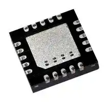
- RF IC Case Style: TQFN
- Receiving Current: 5.5mA
- RF / IF Modulation: ASK, OOK
- Supply Voltage Max: 5.5V
- Supply Voltage Min: 3V
- Operating Temperature Max: 105°C
- Operating Temperature Min: -40°C
- RF Transceiver Applications: Low-Cost RKE, Garage Door Openers, Remote Controls, Home Automation, Sensor N/W, Security Systems
| Delivery and price | |
|---|---|
| Units per pack | 120 |
| Price | 1.05 € |
| Current stock | 200+ |
| Lead time | 7 days |
**EVALUATION KIT AVAILABLE**

## **MAX7036**

## **General Description**

The MAX7036 low-cost receiver is designed to receive amplitude-shift-keyed (ASK) and on-off-keyed (OOK) data in the 300MHz to 450MHz frequency range. The receiver has an RF input signal range of -109dBm to 0dBm.

The MAX7036 requires few external components and has a power-down pin to put it in a low-current sleep mode, making it ideal for cost- and power-sensitive applications. The low-noise amplifier (LNA), phase-locked loop (PLL), mixer, IF filter, received-signal-strength indicator (RSSI), and baseband sections are all on-chip. The MAX7036 uses a very-low intermediate frequency (VLIF) architecture. The MAX7036 integrates the IF filter on-chip and, therefore, eliminates an external ceramic filter, reducing the bill-ofmaterials cost. The device also contains an on-chip automatic gain control (AGC) that reduces the LNA gain by 30dB when the input signal power is large. The MAX7036 operates from either a 5V or a 3.3V power supply and draws 5.5mA (typ) of current.

The MAX7036 is available in a 20-pin thin QFN package with an exposed pad and is specified over the AEC-Q100 Level 2 (-40°C to +105°C) temperature range.

## **Applications**

- Low-Cost RKE

- Garage Door Openers

- Remote Controls

- Home Automation

- Sensor Networks

- Security Systems

## **300MHz to 450MHz ASK Receiver with Internal IF Filter**

## **Benefits and Features**

- ASK/OOK Modulation

- < 250μs Enable Turn-On Time

- On-Chip PLL, VCO, Mixer, IF, Baseband

- Low IF (200kHz Nominal)

- 5.5mA DC Current

- 1μA Standby Current

- 3.3V/5V Operation

- Small 20-Pin Thin QFN Package with an Exposed Pad

- AEC-Q100 Qualified

## **Ordering Information**

||**PART**|**TEMP RANGE**|**PIN-PACKAGE**|
|---|---|---|---|
||MAX7036GTP/V+|-40°C to +105°C|20 Thin QFN-EP*|


_/V denotes an automotive qualified part._

+ _Denotes a lead(Pb)-free/RoHS-compliant package._

* _EP = Exposed pad._

## **Pin Configuration**

**==> picture [242 x 234] intentionally omitted <==**

**----- Start of picture text -----**<br>
TOP VIEW<br>15 14 13 12 11<br>DSP 16 10 IFC1<br>DSN 17 9 IFC2<br>PDOUT 18 MAX7036 8 MIXIN1<br>VDD 19 7 MIXIN2<br>DATAOUT 20 EP 6 LNAOUT<br>+<br>1 2 3 4 5<br>THIN QFN<br>5mm x 5mm<br>DFFB OPP DCOC DVDD IFC3<br>ENABLE XTAL2 XTAL1 AVDD LNAIN<br>**----- End of picture text -----**<br>


**==> picture [125 x 31] intentionally omitted <==**

_19-4386; Rev 2; 8/17_

## MAX7036

## 300MHz to 450MHz ASK Receiver with Internal IF Filter

## **Absolute Maximum Ratings**

VDD to GND...........................................................-0.3V to +6.0V AVDD to GND........................................................-0.3V to +4.0V DVDD to GND........................................................-0.3V to +4.0V ENABLE to GND.........................................-0.3V to (VDD + 0.3V) LNAIN to GND.......................................................-0.3V to +1.2V All Other Pins to GND.............................-0.3V to (VDVDD + 0.3V) Continuous Power Dissipation (TA = +70°C) 20-Pin TQFN (derate 20.8mW/°C above +70°C) ...1666.7mW

Junction-to-Case Thermal Resistance (θJC) (Note 1) 20-Pin TQFN .................................................................2°C/W Junction-to-Ambient Thermal Resistance (θJA) (Note 1) 20-Pin TQFN ...............................................................48°C/W Operating Temperature Range .........................-40°C to +105°C Junction Temperature......................................................+150°C Storage Temperature Range .............................-65°C to +150°C Lead Temperature (soldering, 10s) .................................+300°C Soldering Temperature (reflow) .......................................+260°C

**Note 1:** Package thermal resistances were obtained using the method described in JEDEC specification JESD51-7, using a four-layer board. For detailed information on package thermal considerations, refer to **www.maximintegrated.com/thermal-tutorial** .

_Stresses beyond those listed under “Absolute Maximum Ratings” may cause permanent damage to the device. These are stress ratings only, and functional operation of the device at these or any other conditions beyond those indicated in the operational sections of the specifications is not implied. Exposure to absolute maximum rating conditions for extended periods may affect device reliability._

## **3.3V DC Electrical Characteristics**

( _Typical Application Circuit_ , 50Ω system impedance, VAVDD = VDVDD = VDD = 3.0V to 3.6V, fRF = 300MHz to 450MHz, TA = -40°C to +105°C, unless otherwise noted. Typical values are at VAVDD = VDVDD = VDD = 3.3V, TA = +25°C, unless otherwise noted.) (100% tested at TA = +105°C.)

|tested at TA= +105°C.)||||||
|---|---|---|---|---|---|
|**PARAMETER**|**SYMBOL**|**CONDITIONS**||**MIN**<br>**TYP**<br>**MAX**|**UNITS**|
|Supply Voltage|VDD|VAVDD= VDVDD= VDD||3.0<br>3.3<br>3.6|V|
|Supply Current|IIN|TA< +105°C|fRF= 315MHz|5.3<br>6.7|mA|
||||fRF= 433MHz|5.8<br>7.3||
||||Deep-sleep mode,<br>VENABLE= 0V|1<br>2.7|µA|
|**DIGITAL INPUT (ENABLE)**||||||
|Input High Voltage|VIH|VAVDD= VDVDD= VDD||VDD-<br>0.4|V|
|Input Low Voltage|VIL|VAVDD= VDVDD= VDD||0.4|V|
|Input Current|IENABLE|0 ≤ VENABLE≤ VDD||20|µA|
|**DIGITAL OUTPUT (DATAOUT)**||||||
|Output Low Voltage|VOL|ISINK= 100µA||0.4|V|
|Output High Voltage|VOH|ISOURCE= 100µA||VDD-<br>0.4|V|


Maxim Integrated  │ 2

www.maximintegrated.com

## MAX7036

## 300MHz to 450MHz ASK Receiver with Internal IF Filter

## **5.0V DC Electrical Characteristics**

( _Typical Application Circuit_ , 50Ω system impedance, VDD = 4.5V to 5.5V, fRF = 300MHz to 450MHz, TA = -40°C to +105°C, unless otherwise noted. Typical values are at VDD = 5.0V, TA = +25°C, unless otherwise noted.) (100% tested at TA = +105°C.)

|**PARAMETER**|**SYMBOL**|**CONDITIONS**|**CONDITIONS**|**MIN**<br>**TYP**<br>**MAX**|**UNITS**|
|---|---|---|---|---|---|
|Supply Voltage|VDD|||4.5<br>5.0<br>5.5|V|
|Supply Current|IIN|TA< +105°C|fRF= 315MHz|5.4<br>6.8|mA|
||||fRF= 433MHz|5.9<br>7.4||
||||Deep-sleep mode,<br>VENABLE= 0V|1<br>3.4|µA|
|**DIGITAL INPUT (ENABLE)**||||||
|Input High Voltage|VIH|VAVDD= VDVDD||VDD-<br>0.4|V|
|Input Low Voltage|VIL|VAVDD= VDVDD||0.4|V|
|Input Current|IENABLE|0 ≤ VENABLE≤ VDD||20|µA|
|**DIGITAL OUTPUT (DATAOUT)**||||||
|Output Low Voltage|VOL|ISINK= 100µA||0.4|V|
|Output High Voltage|VOH|ISOURCE= 100µA||VDD-<br>0.4|V|


## **AC Electrical Characteristics**

( _Typical Application Circuit_ , 50Ω system impedance, VAVDD = VDVDD = VDD = 3.0V to 3.6V, fRF = 300MHz to 450MHz, TA = -40°C to +105°C, unless otherwise noted. Typical values are at VAVDD = VDVDD = VDD = 3.3V, TA = +25°C, fRF = 315MHz, unless otherwise noted.) (100% tested at TA = +105°C.)

|**PARAMETER**|**SYMBOL**|**CONDITIONS**|**CONDITIONS**|**MIN**<br>**TYP**<br>**MAX**|**UNITS**|
|---|---|---|---|---|---|
|Receiver Input Frequency Range|fRF|||300<br>450|MHz|
|Maximum Receiver Input Level|PRFIN|||0|dBm|
|Sensitivity (Note 2)||fRF= 315MHz||-109|dBm|
|||fRF= 433MHz||-107||
|Power-On Time|tON|Time for valid RSSI<br>output, does not<br>include baseband<br>flter settling|Enable power on<br>(VDD> 3.0V)|250|µs|
||||VDDpower on|1|ms|
|AGC Hysteresis||||5|dB|
|AGC Low Gain-to-High Gain<br>Switching Time||||13|ms|


Maxim Integrated  │ 3

www.maximintegrated.com

## MAX7036

## 300MHz to 450MHz ASK Receiver with Internal IF Filter

## **AC Electrical Characteristics (continued)**

( _Typical Application Circuit_ , 50Ω system impedance, VAVDD = VDVDD = VDD = 3.0V to 3.6V, fRF = 300MHz to 450MHz, TA = -40°C to +105°C, unless otherwise noted. Typical values are at VAVDD = VDVDD = VDD = 3.3V, TA = +25°C, fRF = 315MHz, unless otherwise noted.) (100% tested at TA = +105°C.)

|**PARAMETER**|**SYMBOL**|**CONDITIONS**|**CONDITIONS**|**MIN**<br>**TYP**<br>**MAX**|**UNITS**|
|---|---|---|---|---|---|
|**LNA/MIXER**||||||
|LNA Input Impedance|ZINLNA|Normalized to 50Ω|fRF= 315MHz|0.4 -<br>j5.6|Ω|
||||fRF= 433MHz|0.4 -<br>j4.0||
|LO Signal Feedthrough to<br>Antenna||||-75|dBm|
|Voltage Gain Reduction||Low-gain mode, AGC|enabled|29|dB|
|LNA/Mixer Voltage Gain||High-gain LNA mode||55|dB|
|||Low-gain LNA mode||26||
|3dB Cutoff Frequency|BWIF|Set by capacitors on IFC1 and IFC2 (see the<br>_Typical Application Circuit_)||400|kHz|
|RSSI Linearity||||±0.5|dB|
|RSSI Dynamic Range||Includes AGC||80|dB|
|RSSI Level||PRFIN< -120dBm||1.34|V|
|||PRFIN> 0dBm, AGC enabled||2.35||
|Intermediate Frequency|fIF|||200|kHz|
|Maximum Data-Filter Bandwidth|BWDF|||50|kHz|
|Maximum Data-Slicer Bandwidth|BWDS|||100|kHz|
|Maximum Peak Detector<br>Bandwidth||||50|kHz|
|Maximum Data Rate||Manchester coded||33|kbps|
|||Nonreturn to zero (NRZ)||66||
|Crystal Frequency|fXTAL|||9.36<br>14.06|MHz|
|Crystal Load Capacitance|CLOAD|||10|pF|


**Note 2:** BER = 2 x 10[-3] , Manchester coded, data rate = 4kbps. IF bandwidth = 400kHz.

Maxim Integrated  │ 4

www.maximintegrated.com

## MAX7036

## 300MHz to 450MHz ASK Receiver with Internal IF Filter

## **Typical Operating Characteristics**

( _Typical Application Circuit_ , VAVDD = VDD = VDVDD = 3.3V, fRF = 315MHz, TA = +25°C, unless otherwise noted.)

**==> picture [498 x 544] intentionally omitted <==**

**----- Start of picture text -----**<br>
SUPPLY CURRENT vs. SUPPLY VOLTAGE SUPPLY CURRENT vs. SUPPLY VOLTAGE<br>(3.3V OPERATION) (5.0V OPERATION) SUPPLY CURRENT vs. RF FREQUENCY<br>5.5 5.45 7.0<br>VAVDD = VDVDD = VDD 5.0V APPLICATION CIRCUIT PRF = -80dBm<br>5.40<br>5.4 Pt ty ————— 6.5 a<br>5.35 TA = +105°C<br>5.3 TA = +85°C<br>fee> 5.30 eee 6.0 e TA = +85°C e<br>5.2 T A  = +85°C 5.25 TA = +105°C<br>TA = +105°C 5.5<br>5.1 gece 5.20 eee<br>TA = +25°C<br>5.0 TA = +25°C 5.15 5.0<br>4.9 oe 5.105.05 Fee T A  = -40°C 4.5 eer TA = +25°C T A  = -40°C<br>TA = -40°C<br>4.8 aoeS ae 5.00 Eee 4.0 ap<br>3.0 3.1 3.2 3.3 3.4 3.5 3.6 4.5 4.7 4.9 5.1 5.3 5.5 250 300 350 400 450 500<br>SUPPLY VOLTAGE (V) SUPPLY VOLTAGE (V) RF FREQUENCY (MHz)<br>BIT ERROR RATE vs. PEAK RF<br>INPUT POWER SENSITIVITY vs. TEMPERATURE RSSI vs. INPUT POWER<br>100 -106.0 2.4<br>fRF = 433MHz -106.5 BER = 0.2% DATA RATE = 4kbps fRF = 433MHz<br>10 -107.0 MANCHESTER 2.2 fIF = 200kHz<br>>] fRF = 315MHz -107.5 OF 2.0 PGF<br>1 POON] eevee fl<br>-108.0<br>Ne ee 1.8 |)<br>-108.5 fRF = 433MHz fRF = 315MHz<br>0.1<br>-109.0 1.6<br>eS es ee e y<br>0.01 een -109.5<br>1.4<br>-110.0<br>0.001 ee -110.5 1.2<br>-125 -120 -115 -110 -105 -40 -15 10 35 60 85 105 -120 -100 -80 -60 -40 -20 0<br>PEAK RF INPUT POWER (dBm) TEMPERATURE (°C) INPUT POWER (dBm)<br>LNA/MIXER VOLTAGE GAIN S11 SMITH CHART PLOT OF RFIN S11 SMITH CHART PLOT OF RFIN<br>vs. IF FREQUENCY (315MHz CIRCUIT) (433MHz CIRCUIT)<br>60<br>PRF = -71dBm<br>58<br>fRF = 433.92MHz<br>56<br>54<br>52<br>50<br>48 S11 = 7.9729Ω - j0.6085 S11 = 6.5175Ω - j5.5849<br>46 at fRF = 315MHz at fRF = 433MHz<br>44<br>N \ J NL<br>42<br>40 PEEEN Le) Le<br>0 200 400 600 800 1000<br>IF FREQUENCY (kHz)<br>MAX7036 toc01 MAX7036 toc02 MAX7036 toc03<br>SUPPLY CURRENT (mA) SUPPLY CURRENT (mA) SUPPLY CURRENT (mA)<br>MAX7036 toc04 MAX7036 toc05 MAX7036 toc06<br>RSSI (V)<br>SENSITIVITY (dBm)<br>BIT ERROR RATE (%)<br>MAX7036 toc07 MAX7036 toc08 MAX7036 toc09<br>LNA/MIXER VOLTAGE GAIN (dB)<br>**----- End of picture text -----**<br>


Maxim Integrated  │ 5

www.maximintegrated.com

## MAX7036

## 300MHz to 450MHz ASK Receiver

## with Internal IF Filter

## **Typical Operating Characteristics (continued)**

( _Typical Application Circuit_ , VAVDD = VDD = VDVDD = 3.3V, fRF = 315MHz, TA = +25°C, unless otherwise noted.)

**==> picture [506 x 534] intentionally omitted <==**

**----- Start of picture text -----**<br>
REGULATOR VOLTAGE PHASE NOISE  PHASE NOISE<br>vs. REGULATOR CURRENT vs. OFFSET FREQUENCY vs. OFFSET FREQUENCY<br>3.15 -50 -50<br>VDD = 5V, +5V CIRCUIT fRF = 315MHz fRF = 433MHz<br>-60 -60<br>-70 -70<br>3.10<br>TA = +105°C -80 -80<br>TA = +85°C TA = +25°C -90 -90<br>3.05 TA = -40°C<br>-100 -100<br>-110 -110<br>3.00 -120 -120<br>0 5 10 15 20 25 0.01 0.1 1 10 100 1000 10,000 0.01 0.1 1 10 100 1000 10,000<br>REGULATOR CURRENT (mA) OFFSET FREQUENCY (kHz) OFFSET FREQUENCY (kHz)<br>Pin Description<br>PIN NAME FUNCTION<br>1 ENABLE Enable Input. Internally pulled down to ground. Set VENABLE = VDD for normal operation.<br>Crystal Input 2. Connect an external crystal from XTAL2 to XTAL1. Bypass to GND if XTAL1 is driven<br>2 XTAL2<br>from an AC-coupled external reference (see the  Crystal Oscillator  section).<br>Crystal Input 1. Connect an external crystal from XTAL2 to XTAL1. Can also be driven with an AC-<br>3 XTAL1<br>coupled external reference oscillator (see the  Crystal Oscillator  section).<br>Positive Analog Supply Voltage. Connect to DVDD. Bypass to GND with a 0.1µF capacitor as close<br>4 AVDD as possible to the device (see the  Typical Application Circuit ). For 5.0V operation, AVDD is internally<br>connected to an on-chip 3.2V LDO regulator. For 3.3V operation, connect AVDD to VDD.<br>5 LNAIN Low-Noise Amplifier Input. Must be AC-coupled (see the  Low-Noise Amplifier  section).<br>6 LNAOUT Low-Noise Amplifier Output. Must be connected to AVDD through a parallel LC tank circuit. AC-couple<br>to MIXIN2 (see the  Low-Noise Amplifier  section).<br>7 MIXIN2 2nd Differential Mixer Input. Connect to the LNAOUT side of the LC tank filter through a 100pF<br>capacitor (see the  Typical Application Circuit ).<br>8 MIXIN1 1st Differential Mixer Input. Connect to the AVDD side of the LC tank filter through a 100pF capacitor<br>(see the  Typical Application Circuit ).<br>9 IFC2 IF Filter Capacitor Connection 2. This is for the Sallen-Key IF filter. Connect a capacitor from IFC2 to GND.<br>The value of the capacitor is determined by the IF filter bandwidth (see the  Typical Application Circuit ).<br>10 IFC1 IF Filter Capacitor Connection 1. This is for the Sallen-Key IF filter. Connect a capacitor from IFC1 to IFC3.<br>The value of the capacitor is determined by the IF filter bandwidth (see the  Typical Application Circuit ).<br>11 IFC3 IF Filter Capacitor Connection 3. This is for the Sallen-Key IF filter. Connect a capacitor from IFC3 to IFC1.<br>The value of the capacitor is determined by the IF filter bandwidth (see the  Typical Application Circuit ).<br>Positive Digital Supply Voltage Input. Connect to AVDD. Bypass to GND with a 0.01µF capacitor as<br>12 DVDD<br>close as possible to the device (see the  Typical Application Circuit ).<br>MAX7036 toc10 MAX7036 toc11 MAX7036 toc12<br>PHASE NOISE (dBc/Hz) PHASE NOISE (dBc/Hz)<br>REGULATOR VOLTAGE (V)<br>**----- End of picture text -----**<br>


Maxim Integrated  │ 6

www.maximintegrated.com

## MAX7036

## 300MHz to 450MHz ASK Receiver

## with Internal IF Filter

## **Pin Description (continued)**

|**PIN**|**NAME**|**FUNCTION**|
|---|---|---|
|13|DCOC|DC Offset Capacitor Connection. This is for the RSSI amplifier. Connect a 1µF capacitor from this pin<br>to ground (see the_Typical Application Circuit_).|
|14|OPP|Noninverting Op-Amp Input. This is for the Sallen-Key data filter. Connect a capacitor from this pin to<br>GND. The value of the capacitor is determined by the data-filter bandwidth.|
|15|DFFB|Data-Filter Feedback Input. Input for the feedback of the Sallen-Key data filter. Connect a capacitor<br>from this pin to DSP. The value of the capacitor is determined by the data-filter bandwidth.|
|16|DSP|Positive Data-Slicer Input. Connect a capacitor from this pin to DFFB. The value of the capacitor is<br>determined by the data-filter bandwidth.|
|17|DSN|Negative Data-Slicer Input|
|18|PDOUT|Peak-Detector Output|
|19|VDD|Power-Supply Voltage Input. For 5.0V operation, VDDis the input to an on-chip voltage regulator<br>whose 3.2V output drives AVDD. Bypass to ground with a 0.1µF capacitor as close as possible to the<br>device (see the_Typical Application Circuit_).|
|20|DATAOUT|Digital Baseband Data Output|
|—|EP|Exposed Pad. Internally connected to ground. Connect to a large ground plane using multiple vias to<br>maximize thermal and electrical performance.|


## **Functional Diagram**

**==> picture [429 x 245] intentionally omitted <==**

**----- Start of picture text -----**<br>
DATAOUT DSN PDOUT DSP OPP DFFB<br>20 17 18 16 14 15<br>XTAL1 3<br>PEAK<br>DETECTOR MAX7036<br>PLL<br>XTAL2 2<br>ENABLE 1<br>VDD 19<br>EP*<br>3.2V ∑<br>REGULATOR<br>AVDD 4 AGC<br>DVDD 12 REF<br>∑<br>LNAIN 5 REF<br>6 8 7 10 9 11 13<br>LNAOUT MIXIN2 IFC1 IFC2 IFC3 DCOC<br>MIXIN1<br>*EXPOSED PAD.<br>CONNECT TO GND.<br>**----- End of picture text -----**<br>


Maxim Integrated  │ 7

www.maximintegrated.com

## MAX7036

## 300MHz to 450MHz ASK Receiver

## with Internal IF Filter

## **Detailed Description**

The MAX7036 CMOS RF receiver, and a few external components, provide the complete receiver chain from the antenna to the digital output data. Depending on signal power and component selection, data rates as high as 33kbps Manchester (66kbps NRZ) can be achieved.

The MAX7036 is designed to receive binary ASK/OOK data modulated in the 300MHz to 450MHz frequency range. ASK modulation uses a difference in amplitude of the carrier to represent digital data.

## **Voltage Regulator**

For operation with a single 3.0V to 3.6V supply voltage, connect AVDD, DVDD, and VDD to the supply voltage. For operation with a single 4.5V to 5.5V supply voltage, connect VDD to the supply voltage. An on-chip voltage regulator drives the AVDD pin to approximately 3.2V. For proper operation, connect DVDD and AVDD together. Bypass VDD and AVDD to GND with 0.1μF capacitors placed as close as possible to the device. Bypass DVDD to GND with a 0.01μF capacitor (see the _Typical Application Circuit_ ).

## **Low-Noise Amplifier**

The LNA is an nMOS cascode amplifier. The LNA and mixer have a combined 55dB voltage gain. The gain and noise figures are dependent on both the antennamatching network at the LNA input and the LC tank network between the LNA output and the mixer inputs.

L2 and C1 comprise the LC tank filter connected to LNAOUT (see the _Typical Application Circuit_ ). L2 also serves as a bias inductor to LNAOUT. Bypass the powersupply side of L2 to GND with a capacitor that provides a low-impedance path at the RF carrier frequency (e.g., 220pF). Select L2 and C1 to resonate at the desired RF input frequency. The resonant frequency is given by:

**==> picture [124 x 25] intentionally omitted <==**

where LTOTAL = L2 + LPARASITICS and CTOTAL = C1 + CPARASITICS.

LPARASITICS and CPARASITICS include inductance and capacitance of the PCB traces, package pins, mixer input impedance, LNA output impedance, etc. At high frequencies, these parasitics can have a dramatic effect on the tank filter center frequency and must not be ignored. The total parasitic capacitance is generally 4pF to 6pF. Adjust L2 and C1 accordingly to achieve the desired tank center frequency.

## **Automatic Gain Control (AGC)**

The AGC circuit monitors the RSSI output. The AGC switches to its low-gain state when the RSSI output reaches 2.2V. The AGC gain reduction is typically 29dB, corresponding to an RSSI voltage drop of 435mV. The LNA resumes high-gain mode when the RSSI level drops back below 1.67V for 13ms for 315MHz and 10ms for 433MHz operation. The AGC has a hysteresis of 5dB. With this AGC function, the MAX7036 can reliably produce an ASK output for RF input levels up to 0dBm, with modulation depth of 30dB.

## **Mixer**

The mixer cell is a double-balanced mixer that performs a downconversion of the RF input to a typical IF of 200kHz from either a high-side or a low-side injected LO. The mixer output drives the input of the on-chip IF filter.

## **Phase-Locked Loop (PLL)**

The PLL block contains a phase detector, charge pump, integrated loop filter, VCO, asynchronous clock dividers, and crystal-oscillator driver. Besides the crystal, this PLL does not require any external components. The VCO generates the LO. The relationship between the RF, IF, and crystal reference frequencies is given by:

**==> picture [55 x 24] intentionally omitted <==**

where fLO = fRF ± fIF

## **Received-Signal-Strength Indicator (RSSI)**

The RSSI circuit provides a DC output proportional to the logarithm of the input power level. RSSI output voltage has a slope of about 14.5mV/dB (of input power). The RSSI monotonic dynamic range exceeds 80dB. This includes the 30dB of AGC.

## **Applications Information**

## **Crystal Oscillator**

The crystal (XTAL) oscillator in the MAX7036 is designed to present a capacitance of approximately 4pF between XTAL1 and XTAL2. In most cases, this corresponds to a 6pF load capacitance applied to the external crystal when typical PCB parasitics are added. The MAX7036 is designed to operate with a typical 10pF load capacitance crystal. **It is very important to use a crystal with a load capacitance equal to the capacitance of the MAX7036 crystal oscillator plus PCB parasitics.** If a crystal designed to oscillate with a different load capacitance is used, the crystal is pulled away from its stated operating

Maxim Integrated  │ 8

www.maximintegrated.com

## MAX7036

frequency, introducing an error in the reference frequency. A crystal designed to operate at a higher load capacitance than the value specified for the oscillator is always pulled higher in frequency. Adding capacitance to increase the load capacitance on the crystal increases the start-up time and may prevent oscillation altogether.

In actuality, the oscillator pulls every crystal. The crystal’s natural frequency is really below its specified frequency, but when loaded with the specified load capacitance, the crystal is pulled and oscillates at its specified frequency. This pulling is already accounted for in the specification of the load capacitance.

Additional pulling can be calculated if the electrical parameters of the crystal are known. The frequency pulling is given by:

**==> picture [225 x 28] intentionally omitted <==**

## 300MHz to 450MHz ASK Receiver with Internal IF Filter

Because the stray shunt capacitance at each of the pins (IFC1 and IFC2) on a typical PCB is approximately 2pF, choose the value of the external capacitors to be approximately 2pF lower than the desired total capacitance. Therefore, the practical values for C9 and C10 are 22pF and 10pF, respectively.

**==> picture [127 x 87] intentionally omitted <==**

**----- Start of picture text -----**<br>
MAX7036<br>22kΩ 22kΩ<br>10 9 11<br>IFC1 IFC2 IFC3<br>C10<br>C9<br>**----- End of picture text -----**<br>


where:

fp is the amount the crystal frequency is pulled in ppm.

_Figure 1. Sallen-Key Lowpass IF Filter_

CM is the motional capacitance of the crystal.

CCASE is the case capacitance.

CSPEC is the specified load capacitance.

CLOAD is the actual load capacitance.

When the crystal is loaded, as specified (i.e., CLOAD = CSPEC), the frequency pulling equals zero.

It is possible to use an external reference oscillator in place of a crystal to drive the VCO. AC-couple the external oscillator to XTAL1 with a 1000pF capacitor. Drive XTAL1 with a signal level of approximately -10dBm. AC-couple XTAL2 to ground with a 1000pF capacitor.

## **IF Filter**

The IF filter is a 2nd-order Butterworth lowpass filter preceded by a low-frequency DC block. The lowpass filter is implemented as a Sallen-Key filter using an internal op amp and two on-chip 22kΩ resistors. The pole locations are set by the combination of the on-chip resistors and two external capacitors (C9 and C10, Figure 1). The values of these two capacitors for a 3dB cutoff frequency of 400kHz are given below:

**==> picture [235 x 49] intentionally omitted <==**

## **Data Filter**

The data filter is implemented as a 2nd-order lowpass Sallen-Key filter. The pole locations are set by the combination of two on-chip resistors and two external capacitors. Adjusting the value of the external capacitors changes the corner frequency to optimize for different data rates. Set the corner frequency to approximately 1.5 times the fastest Manchester expected data rate from the transmitter. Keeping the corner frequency near the data rate rejects any noise at higher frequencies, resulting in an increase in receiver sensitivity.

The configuration shown in Figure 2 can create a Butterworth or Bessel response. The Butterworth filter offers a very flat amplitude response in the passband and a rolloff rate of 40dB/decade for the two-pole filter. The Bessel filter has a linear phase response, which works with the coefficients in Table 1.

**==> picture [81 x 65] intentionally omitted <==**

where fC is the desired corner frequency.

Maxim Integrated  │ 9

www.maximintegrated.com

## MAX7036

## 300MHz to 450MHz ASK Receiver

## with Internal IF Filter

For example, to choose a Butterworth filter response with a corner frequency of 6kHz:

**==> picture [175 x 54] intentionally omitted <==**

Choosing standard capacitor values changes C5 to 390pF and C6 to 180pF, as shown in the _Typical Application Circuit_ .

## **Table 1. Coefficients to Calculate C5 and C6**

|**and C6**|||
|---|---|---|
|**FILTER TYPE**|**a**|**b**|
|Butterworth (Q = 0.707)|1.414|1.000|
|Bessel (Q = 0.577)|1.3617|0.618|


**==> picture [242 x 157] intentionally omitted <==**

**----- Start of picture text -----**<br>
MAX7036<br>RSSI<br>RDF2 RDF1<br>100kΩ 100kΩ<br>16 14 15<br>DSP OPP DFFB<br>C6 C5<br>**----- End of picture text -----**<br>


_Figure 2. Sallen-Key Lowpass Data Filter_

## **Data Slicer**

The data slicer takes the analog output of the data filter and converts it to a digital signal. This is achieved by using a comparator and comparing the analog input to a threshold voltage. One input is supplied by the data-filter output. Both comparator inputs are accessible off chip to allow for different methods of generating the slicing threshold, which is applied to the second comparator input.

The suggested data-slicer configuration uses a resistor (R1) connected between DSN and DSP with a capacitor (C4) from DSN to GND (Figure 3). This configuration averages the analog output of the filter and sets the threshold to approximately 50% of that amplitude. With this configuration, the threshold automatically adjusts as the analog signal varies, minimizing the possibility for errors in the digital data. The values of R1 and C4 affect how fast the threshold tracks to the analog amplitude. Be sure to keep the corner frequency of the RC circuit much lower than the lowest expected data rate.

**==> picture [242 x 156] intentionally omitted <==**

**----- Start of picture text -----**<br>
MAX7036<br>DATA<br>FILTER<br>DATA<br>SLICER<br>20 17 16<br>DSN DSP<br>R1<br>DATAOUT<br>C4<br>**----- End of picture text -----**<br>


_Figure 3. Generating Data-Slicer Threshold_

Note that a long string of zeros or ones can cause the threshold to drift. This configuration works best if a coding scheme (e.g., Manchester coding, which has an equal number of zeros and ones) is used.

## **Peak Detector**

The peak-detector output (PDOUT), in conjunction with an external RC filter, creates a DC output voltage equal to the peak value of the data signal. The resistor provides a path for the capacitor to discharge, allowing the peak detector to dynamically follow peak changes of the datafilter output voltage. The peak detector can be used for at least two functions. First, it can serve as an RSSI for ASK modulation. Second, it can be used for faster data-slicer response by adding it to the threshold pin (DSN) on the data-slicer comparator (Figure 4). The two capacitors in this circuit should be equal, and the peak detector resistor should be approximately 10 times larger than the resistor

Maxim Integrated  │ 10

www.maximintegrated.com

## MAX7036

in the RC smoothing circuit between DSP and DSN. This circuit will provide an instantaneous jump of one-half of the DSP increase from “no signal” voltage to peak voltage, which then decays with the same time constant as that of the threshold build-up from the RC smoothing circuit. The DC slicing voltage at DSN is slightly higher (by the ratio of the two resistors in the circuit) than it would be without the speed-up circuit. **Always provide a capacitive path from the PDOUT pin to ground when using the peak-detector output.**

**==> picture [242 x 174] intentionally omitted <==**

**----- Start of picture text -----**<br>
DATA<br>FILTER<br>MAX7036<br>DATA<br>SLICER<br>20 17 16 18<br>DSN DSP PDOUT<br>R1<br>DATAOUT<br>C4<br>**----- End of picture text -----**<br>


_Figure 4. Using PDOUT for Faster Startup_

## **Layout Considerations**

A properly designed PCB is an essential part of any RF/ microwave circuit. On high-frequency inputs and outputs, use controlled-impedance lines and keep them as short as possible to minimize losses and radiation. At high frequencies, trace lengths that are λ/10 or longer act as antennas.

## 300MHz to 450MHz ASK Receiver with Internal IF Filter

Keeping the traces short also reduces parasitic inductance. Generally, 1in of a PCB trace adds about 20nH of parasitic inductance. The parasitic inductance can have a dramatic effect on the effective inductance of a passive component. For example, a 0.5in trace connecting a 100nH inductor adds an extra 10nH of inductance or 10%.

To reduce the parasitic inductance, use wider traces and a solid ground or power plane below the signal traces. Also, use low-inductance connections to ground on all GND pins, and place decoupling capacitors close to all power-supply connections.

**Table 2. Component Values**

|**COMPONENT**|**fRF = 315MHz**|**fRF = 433.92MHz**|
|---|---|---|
|C1|4.7pF|2.7pF|
|C2|100pF|100pF|
|C3|100pF|100pF|
|C4|0.1µF|0.1µF|
|C5|390pF|390pF|
|C6|180pF|180pF|
|C7|1µF|1µF|
|C8|0.01µF|0.01µF|
|C9|22pF|22pF|
|C10|10pF|10pF|
|C11|0.1µF|0.1µF|
|C12|220pF|220pF|
|C13|10pF|10pF|
|C14|10pF|10pF|
|C15|100pF|100pF|
|C16|0.1µF|0.1µF|
|L1|100nH|47nH|
|L2|27nH|15nH|
|R1|22kΩ|22kΩ|
|Y1|9.8375MHz|13.55375MHz|


Maxim Integrated  │ 11

www.maximintegrated.com

## MAX7036

## 300MHz to 450MHz ASK Receiver with Internal IF Filter

## **Typical Application Circuit**

**==> picture [403 x 374] intentionally omitted <==**

**----- Start of picture text -----**<br>
IF VSUP IS THEN V3V IS<br>3.0V TO 3.6V TIED TO VSUP<br>R2 C17<br>CREATED BY LDO,<br>V3V 4.5V TO 5.5V AVAILABLE AT VSUP<br>AVDD (PIN 4)<br>R1<br>(SEE TABLE ABOVE)<br>C11 C4<br>C5<br>f- t | | := ] —<br>DATAOUT VDD PDOUT DSN DSP<br>ENABLE DFFB<br>XTAL2 OPP<br>C13 Y1 C6<br>C14<br>XTAL1 MAX7036 DCOC<br>C7<br>zt i<br>AVDD DVDD<br>C16 C8<br>L1 C15<br>LNAIN IFC3<br>LNAOUT MIXIN2 MIXIN1 IFC2 IFC1<br>C9<br>C3 C2 C10<br>C1 L2<br>P ere<br>C12<br>**----- End of picture text -----**<br>


## **Chip Information**

PROCESS: CMOS

## **Package Information**

For the latest package outline information and land patterns (footprints), go to **www.maximintegrated.com/packages** . Note that a “+”, “#”, or “-” in the package code indicates RoHS status only. Package drawings may show a different suffix character, but

the drawing pertains to the package regardless of RoHS status.

|**PACKAGE**<br>**TYPE**<br>~~pf~~|**PACKAGE**<br>**CODE**<br>~~pfff~~|**OUTLINE**<br>**NO.**<br>~~ff~~|**LAND**<br>**PATTERN**<br>**NO.**<br>~~ff~~|
|---|---|---|---|
|20 Thin QFN-EP<br>~~pf~~|T2055+3<br>~~pfff~~|**21-0140**<br>~~ff~~|**90-0008**<br>~~ff~~|


Maxim Integrated  │ 12

www.maximintegrated.com

## MAX7036

## 300MHz to 450MHz ASK Receiver

## with Internal IF Filter

## **Revision History**

|**Revision**|**History**|||
|---|---|---|---|
|**REVISION**<br>**NUMBER**|**REVISION**<br>**DATE**|**DESCRIPTION**|**PAGES**<br>**CHANGED**|
|0|3/09|Initial release|—|
|1|8/10|Updated_Absolute Maximum Ratings_, TOCs 5, 11, and 12,_Pin Description_,<br>_Phase-Locked Loop (PLL)_and_Crystal Oscillator_sections, and_Typical_<br>_Application Circuit_|2, 5, 6, 8, 9, 12|
|2|8/17|Added AEC-Q100 qualifcation statement to_Benefts and Features_section|1|


For pricing, delivery, and ordering information, please contact Maxim Direct at 1-888-629-4642, or visit Maxim Integrated’s website at www.maximintegrated.com.

_Maxim Integrated cannot assume responsibility for use of any circuitry other than circuitry entirely embodied in a Maxim Integrated product. No circuit patent licenses are implied. Maxim Integrated reserves the right to change the circuitry and specifications without notice at any time. The parametric values (min and max limits) shown in the Electrical Characteristics table are guaranteed. Other parametric values quoted in this data sheet are provided for guidance._

© 2017 Maxim Integrated Products, Inc.  │ 13

Maxim Integrated and the Maxim Integrated logo are trademarks of Maxim Integrated Products, Inc.
Updated at February 9, 2023
Since its inception in 1965, Analog Devices has established itself as a global leader in the design and manufacturing of high-performance analog, mixed-signal, and digital signal processing (DSP) integrated circuits. The company is renowned for solving complex engineering challenges by providing critical technologies that seamlessly convert real-world phenomena into precise electrical signals for the industrial, automotive, communications, and consumer markets. Within its extensive portfolio, Analog Devices provides highly reliable clock, timing, and frequency management solutions, featuring a comprehensive array of precision timers, oscillators, and pulse generators. Complementing this core lineup is a robust offering of driver and interface ICs, particularly high-performance I/O expanders that enable seamless connectivity and streamline complex electronic system architectures. Beyond these foundational integrated circuits, Analog Devices leads the industry in sensor innovation, delivering advanced MEMS accelerometers and integrated MEMS modules designed for exceptional precision in motion sensing. To support complete hardware designs, the company's specialized offerings also encompass discrete bipolar transistors, sub-2.4GHz RF transceivers, temperature-compensated oscillators, and dedicated power management components such as DC/DC converters and LED driver ICs.
About Novapart
Novapart is a B2B electronic component broker specialising in stock shortages and cost reduction. We source hard-to-find parts and identify compliant alternatives across a catalogue of 410,000+ components from 500+ manufacturers.
Learn more →Stock Shortage Specialist
When a component is unavailable, discontinued or has an unacceptable lead time, we tap into our network of vetted European and Asian distributors to source what you need — without compromising on quality or traceability.
Request a quote →Compliant Alternatives
We identify pin-to-pin, electrically equivalent substitutes that meet the same certifications (RoHS, AEC-Q100, REACH) as your original specification — validated against datasheets, not just part numbers. Often at a lower cost.
BOM Analysis service →