
Image not available
Illustrative purposes only

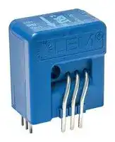
LXS 25-NPS
Current Transducer, LXS Series, 25 A, -85A to 85A, 0.45 %, Voltage Output, 4.75 Vdc to 5.25 Vdc
⚠️ Reference pricing provided. In case of supply shortages, we will connect you with our trusted procurement partners to ensure your project's continuity.
- Manufacturer: LEM
- Product type: Current Sensors
- SVHC: No SVHC (25-Jun-2025)
- Accuracy: ± 0.5%
- Accuracy %: 0.45%
- Product Range: LXS Series
- Response Time: 0.4µs
- Primary Current: 25A
- Sensor Mounting: Through Hole
- Measured Current: AC / DC / Pulsed
- Sensor Output Type: Voltage
- Supply Voltage Range: 4.75V to 5.25V
- Secondary Signal Type: 2.5V
- Supply Voltage DC Max: 5.25V
- Supply Voltage DC Min: 4.75V
- Current Sensor Technology: Closed Loop, Hall Effect
- Operating Temperature Max: 105°C
- Operating Temperature Min: -40°C
- Current Measuring Range AC: -85A to 85A
- Current Measuring Range DC: -85A to 85A
| Delivery and price | |
|---|---|
| Units per pack | 50 |
| Price | 9.5 € |
| Current stock | 10+ |
| Lead time | 30 days |
Datasheet

## **Current Transducer LXS series**

## _I_ **= 6, 15, 25 A** P N

## **Ref: LXS 6-NPS, LXS 15-NPS, LXS 25-NPS**

For the electronic measurement of current: DC, AC, pulsed..., with galvanic separation between the primary and the secondary circuit.

## **Features**

- ●Closed loop multi-range current transducer

- ●Voltage output

- ●Unipolar supply voltage

- ●Compact design for PCB mounting.

## **Advantages**

- ●Very low offset drift

## **Applications**

   - ●AC variable speed and servo motor drives

   - ●Static converters for DC motor drives

   - ●Battery supplied applications

   - ●Uninterruptible Power Supplies (UPS)

   - ●Switched Mode Power Supplies (SMPS)

   - ●Power supplies for welding applications

   - ●Solar inverters.

- ●Very good d _v_ /d _t_ immunity

- ●LTS footprint compatible

- ●Extended measuring range for unipolar measurement.

## **Standards**

- ●IEC 61800-1: 1997

- ●IEC 61800-2: 2015

- ●IEC 61800-3: 2004

- ●IEC 61800-5-1: 2007

- ●IEC 62109-1: 2010

- ●IEC 62477-1: 2012

- ●UL 508:2013

## **Application Domain**

- ●Industrial.

N°97.O9.09.000.0, N°97.O9.15.000.0, N°97.O9.19.000.0

Page 1/16

LEM reserves the right to carry out modifications on its transducers, in order to improve them, without prior notice

11July2018/Version 1

www.lem.com

**LXS SERIES**

## **Absolute maximum ratings**

**==> picture [512 x 23] intentionally omitted <==**

**----- Start of picture text -----**<br>
Parameter Symbol Unit Value<br>**----- End of picture text -----**<br>


|**Parameter**|**Symbol**|**Unit**|**Value**|
|---|---|---|---|
|||||
|Maximum supply voltage|_U_C max|V|7|
|Maximum primary conductor temperature|_T_B max|°C|110|
|Maximum primary current|_I_P max|A|20 ×_I_PN|
|Maximum electrostatic discharge voltage|_U_ESD max|kV|4|


Stresses above these ratings may cause permanent damage. Exposure to absolute maximum ratings for extended periods may degrade reliability.

## **UL 508: Ratings and assumptions of certification**

File # E189713 Volume: 2 Section: 11

## **Standards**

- ●CSA C22.2 NO. 14-10 INDUSTRIAL CONTROL EQUIPMENT - Date 2011/08/01

- ●UL 508 STANDARD FOR INDUSTRIAL CONTROL EQUIPMENT - Date 2013

## **Ratings**

**==> picture [512 x 20] intentionally omitted <==**

**----- Start of picture text -----**<br>
Parameter Symbol Unit Value<br>**----- End of picture text -----**<br>


|**Parameter**|**Symbol**|**Unit**|**Value**|
|---|---|---|---|
|||||
|Primary involved potential||V AC/DC|600|
|Max surrounding air temperature|_T_A|°C|105|
|Primary current|_I_P|A|According to series primary<br>currents|
|Secondary supply voltage|_U_C|V DC|7|
|Output voltage|_V_out|V|0 to 5|


## **Conditions of acceptability**

When installed in the end-use equipment, consideration shall be given to the following:

- _1 - These devices must be mounted in a suitable end-use enclosure._

- _2 -  The terminals have not been evaluated for field wiring._

- _3 - The LES, LESR, LKSR, LPSR, LXS and LXSR Series shall be used in a pollution degree 2 environment or better._

- _4 -  Low voltage circuits are intended to be powered by a circuit derived from an isolating source (such as a transformer, optical isolator, limiting impedance or electro-mechanical relay) and having no direct connection back to the primary circuit (other than through the grounding means)._

- _5 -  These devices are intended to be mounted on the printed wiring board of the end-use equipment (with a minimum CTI of 100)._

- _6 -  LES, LESR, LKSR and LPSR Series: based on results of temperature tests, in the end-use application, a maximum of 110°C cannot be exceeded on the primary jumper._

## **Marking**

Only those products bearing the UL or UR Mark should be considered to be Listed or Recognized and covered under UL’s FollowUp Service. Always look for the Mark on the product.

Page 2/16

LEM reserves the right to carry out modifications on its transducers, in order to improve them, without prior notice

11July2018/Version 1

www.lem.com

**LXS SERIES**

## **Insulation coordination**

**==> picture [512 x 25] intentionally omitted <==**

**----- Start of picture text -----**<br>
Parameter Symbol Unit Value Comment<br>**----- End of picture text -----**<br>


|**Parameter**|**Symbol**|**Unit**|**Value**|**Comment**|
|---|---|---|---|---|
||||||
|RMS voltage for AC insulation test, 50 Hz, 1 min|_U_d|kV|4.3||
|Impulse withstand voltage 1.2/50 μs|_Û_W|kV|8||
|Insulation resistance|_R_INS|GΩ|18|measured at 500 V DC|
|Partial discharge RMS test voltage (_q_m< 10 pC)|_U_t|kV|1.65||
|Clearance (pri. - sec.)|_d_CI|mm||See dimensions drawing on<br>page 19|
|Creepage distance (pri. - sec.)|_d_Cp||||
|Case material|-|-|V0|According to UL 94|
|Comparative tracking index|_CTI_||600||
|Application example||V|300 V<br>CAT III, PD2|Reinforced insulation, non<br>uniform feld according to<br>IEC 61800-5-1|
|Application example||V|600 V<br>CAT III, PD2|Basic insulation, non<br>uniform feld according to<br>IEC 61800-5-1|


## **Environmental and mechanical characteristics**

|**Parameter**|**Symbol**|**Unit**|**Min**|**Typ**|**Max**|**Comment**|
|---|---|---|---|---|---|---|
|Ambient operating temperature|_T_A|°C|−40||105||
|Ambient storage temperature|_T_S|°C|−55||125||
|Mass|_m_|g||10|||


Page 3/16 www.lem.com

LEM reserves the right to carry out modifications on its transducers, in order to improve them, without prior notice

11July2018/Version 1

**LXS SERIES**

## **Electrical data LXS 6-NPS**

At _T_ A = 25 °C, _U_ C = +5 V, _N_ P = 1 turn, _R_ L = 10 kΩ internal reference, unless otherwise noted (see Min, Max, typical definition paragraph in page 18).

**==> picture [513 x 22] intentionally omitted <==**

**----- Start of picture text -----**<br>
Parameter Symbol Unit Min Typ Max Comment<br>**----- End of picture text -----**<br>


|**Parameter**|**Symbol**|**Unit**|**Min**|**Typ**|**Typ**|**Max**|**Comment**|
|---|---|---|---|---|---|---|---|
|||||||||
|Primary nominal RMS current|_I_P N|A||6|||Apply derating according<br>to fg. 16|
|Primary current, measuring range|_I_P M|A|−20|||20||
|Number of primary turns|_N_P|||1, 2, 3||||
|Supply voltage|_U_C|V|4.75||5|5.25||
|Current consumption|_I_C|mA||18 +|)<br>(<br>_N_<br>mA<br>_I_<br>S<br>P<br>|)<br>(<br>_N_<br>mA<br>_I_<br>S<br>P<br>20.5 +|_N_S= 2000 turns|
|Output voltage|_V_out|V|0.25|||4.75|with_U_C= +5 V|
|Output voltage @_I_P= 0 A|_V_out|V|||2.5|||
|Electrical ofset voltage|_V_O E|mV|−19.8|||19.8|100 % tested_V_out− 2.5 V|
|Electrical ofset current<br>referred to primary|_I_O E|mA|−190|||190|100 % tested|
|Temperature coefcient of_V_out<br>@_I_P= 0 A|_TCV_out|ppm/K||||±70|ppm/K of 2.5 V<br>−40 °C ... 105 °C|
|Theoretical sensitivity|_G_th|mV/A||104.2|||625 mV/_I_P N|
|Sensitivity error|_εG_|%|−0.2|||0.2|100 % tested|
|Temperature coefcient of_G_|_TCG_|ppm/K||||±45|−40 °C ... 105 °C|
|Linearity error|_ε_L|% of_I_P N|−0.1|||0.1||
|Magnetic ofset current (10 ×_I_P N)<br>referred to primary|_I_O M|mA|−25|||25||
|Output RMS noise current<br>100 Hz … 100 kHz|_e_no|µV/Hz½||7||||
|Output noise voltage<br>DC ... 10 kHz<br>DC ... 100 kHz<br>DC ... 1 MHz|_V_no|mVpp||11.5<br>13.6<br>13.8||||
|Reaction time @ 10 % of_I_P N|_t_ra|µs||||0.3|_R_L= 1 kΩ, d_i_/d_t_= 50 A/µs|
|Step response time to 90 % of_I_P N|_t_r|µs||||0.4|_R_L= 1 kΩ, d_i_/d_t_= 50 A/µs|
|Frequency bandwidth (±3 dB)|_BW_|kHz|300||||_R_L= 1 kΩ|
|Overall accuracy|_X_G|% of_I_P N||||3.2||
|Overall accuracy @_T_A= 85 °C<br>(105 °C)|_X_G|% of_I_P N||||3.5 (4.2)||
|Accuracy|_X_|% of_I_P N||||0.45||
|Accuracy @_T_A= 85 °C (105 °C)|_X_|% of_I_P N||||0.8 (1)||


Page 4/16

LEM reserves the right to carry out modifications on its transducers, in order to improve them, without prior notice

11July2018/Version 1

www.lem.com

**LXS SERIES**

## **Electrical data LXS 15-NPS**

At _T_ A = 25 °C, _U_ C = +5 V, _N_ P = 1 turn, _R_ L = 10 kΩ internal reference, unless otherwise noted (see Min, Max, typical definition paragraph in page 18).

**==> picture [513 x 22] intentionally omitted <==**

**----- Start of picture text -----**<br>
Parameter Symbol Unit Min Typ Max Comment<br>**----- End of picture text -----**<br>


|**Parameter**|**Symbol**|**Unit**|**Min**|**Typ**|**Typ**|**Max**|**Comment**|
|---|---|---|---|---|---|---|---|
|||||||||
|Primary nominal RMS current|_I_P N|A||15|||Apply derating according<br>to fg. 17|
|Primary current, measuring range|_I_P M|A|−51|||51||
|Number of primary turns|_N_P|||1, 2, 3||||
|Supply voltage|_U_C|V|4.75||5|5.25||
|Current consumption|_I_C|mA||18 +|)<br>(<br>_N_<br>mA<br>_I_<br>S<br>P<br>|)<br>(<br>_N_<br>mA<br>_I_<br>S<br>P<br>20.5 +|_N_S= 2000 turns|
|Output voltage|_V_out|V|0.25|||4.75|with_U_C= +5 V|
|Output voltage @_I_P= 0 A|_V_out|V|||2.5|||
|Electrical ofset voltage|_V_O E|mV|−15.42|||15.42|100 % tested_V_out− 2.5 V|
|Electrical ofset current<br>referred to primary|_I_O E|mA|−370|||370|100 % tested|
|Temperature coefcient of_V_out<br>@_I_P= 0 A|_TCV_out|ppm/K||||±80|ppm/K of 2.5 V<br>−40 °C … 105 °C|
|Theoretical sensitivity|_G_th|mV/A||41.67|||625 mV_I_P N|
|Sensitivity error|_εG_|%|−0.2|||0.2|100 % tested|
|Temperature coefcient of_G_|_TCG_|ppm/K||||±45|−40 °C … 105 °C|
|Linearity error|_ε_L|% of_I_P N|−0.1|||0.1||
|Magnetic ofset current (10 ×_I_P N)<br>referred to primary|_I_O M|mA|−45|||45||
|Output RMS noise current<br>100 Hz … 100 kHz|_e_no|µV/Hz½||4||||
|Output noise voltage<br>DC ... 10 kHz<br>DC ... 100 kHz<br>DC ... 1 MHz|_V_no|mVpp||5.7<br>6.3<br>7.6||||
|Reaction time @ 10 % of_I_P N|_t_ra|µs||||0.3|_R_L= 1 kΩ, d_i_/d_t_= 50 A/µs|
|Step response time to 90 % of_I_P N|_t_r|µs||||0.4|_R_L= 1 kΩ, d_i_/d_t_= 50 A/µs|
|Frequency bandwidth (±3 dB)|_BW_|kHz|300||||_R_L= 1 kΩ|
|Overall accuracy|_X_G|% of_I_P N||||2.5||
|Overall accuracy @_T_A= 85 °C<br>(105 °C)|_X_G|% of_I_P N||||3 (3.9)||
|Accuracy|_X_|% of_I_P N||||0.45||
|Accuracy @_T_A= 85 °C (105 °C)|_X_|% of_I_P N||||0.7 (0.75)||


Page 5/16

LEM reserves the right to carry out modifications on its transducers, in order to improve them, without prior notice

11July2018/Version 1

www.lem.com

**LXS SERIES**

## **Electrical data LXS 25-NPS**

At _T_ A = 25 °C, _U_ C = +5 V, _N_ P = 1 turn, _R_ L = 10 kΩ internal reference, unless otherwise noted (see Min, Max, typical definition paragraph in page 18).

**==> picture [513 x 22] intentionally omitted <==**

**----- Start of picture text -----**<br>
Parameter Symbol Unit Min Typ Max Comment<br>**----- End of picture text -----**<br>


|**Parameter**|**Symbol**|**Unit**|**Min**|**Typ**|**Typ**|**Max**|**Comment**|
|---|---|---|---|---|---|---|---|
|||||||||
|Primary nominal RMS current|_I_P N|A||25|||Apply derating according<br>to fg. 18|
|Primary current, measuring range|_I_P M|A|−85|||85||
|Number of primary turns|_N_P|||1, 2, 3||||
|Supply voltage|_U_C|V|4.75||5|5.25||
|Current consumption|_I_C|mA||18 +|)<br>(<br>_N_<br>mA<br>_I_<br>S<br>P<br>|)<br>(<br>_N_<br>mA<br>_I_<br>S<br>P<br>20.5 +|_N_S= 2000 turns|
|Output voltage|_V_out|V|0.25|||4.75|with_U_C= +5 V|
|Output voltage @_I_P= 0 A|_V_out|V|||2.5|||
|Electrical ofset voltage|_V_O E|mV|−14.5|||14.5|100 % tested _V_out−  2.5 V|
|Electrical ofset current<br>referred to primary|_I_O E|mA|−580|||580|100 % tested|
|Temperature coefcient of_V_out<br>@_I_P= 0 A|_TCV_out|ppm/K||||±80|ppm/K of 2.5 V<br>−40 °C … 105 °C|
|Theoretical sensitivity|_G_th|mV/A|||25||625 mV_I_P N|
|Sensitivity error|_εG_|%|−0.2|||0.2|100 % tested|
|Temperature coefcient of_G_|_TCG_|ppm/K||||±45|−40 °C … 105 °C|
|Linearity error|_ε_L|% of_I_P N|−0.1|||0.1||
|Magnetic ofset current (10 ×_I_P N)<br>referred to primary|_I_O M|mA|−60|||60||
|Output RMS noise current<br>100 Hz … 100 kHz|_e_no|µV/Hz½|||3.5|||
|Output noise voltage<br>DC ... 10 kHz<br>DC ... 100 kHz<br>DC ... 1 MHz|_V_no|mVpp|||2.7<br>4.5<br>5.3|||
|Reaction time @ 10 % of_I_P N|_t_ra|µs||||0.3|_R_L= 1 kΩ, d_i_/d_t_= 50 A/µs|
|Step response time to 90 % of_I_P N|_t_r|µs||||0.4|_R_L= 1 kΩ, d_i_/d_t_= 50 A/µs|
|Frequency bandwidth (±3 dB)|_BW_|kHz|300||||_R_L= 1 kΩ|
|Overall accuracy|_X_G|% of_I_P N||||2.5||
|Overall accuracy @_T_A= 85 °C<br>(105 °C)|_X_G|% of_I_P N||||3 (3.1)||
|Accuracy|_X_|% of_I_P N||||0.45||
|Accuracy @_T_A= 85 °C (105 °C)|_X_|% of_I_P N||||0.7 (0.75)||


Page 6/16

LEM reserves the right to carry out modifications on its transducers, in order to improve them, without prior notice

11July2018/Version 1

www.lem.com

**LXS SERIES**

## **Typical performance characteristics LXS 6-NPS**

**==> picture [497 x 604] intentionally omitted <==**

**----- Start of picture text -----**<br>
0.1<br>4 Rel. Sensitivity 20<br>Phase<br>2 10<br>0.05<br>0 0<br>− 2 −10<br>0<br>− 4 −20<br>−0.05 − 6 −30<br>− 8 −40<br>−0.1 −1 0 −50<br>−6 6 101 102 103 104 105 106<br>I P [A] Frequency [Hz]<br>Figure 1:  Linearity error Figure 2: Frequency response<br>6 0.625<br>4 0.417<br>I P<br>V out−2.5<br>2 0.208<br>0 0<br>100 200 300 400 500<br>t  ( µ s)<br>Figure 3: Step response<br>10000 3.5<br>3.4<br>600<br>3.3<br>1000 3.2<br>3.1<br>400 3.0<br>100 V P 2.9<br>V out 2.8<br>200 2.7<br>10 2.6<br>2.5<br>2.4<br>0 20 k V / µ s<br>2.3<br>1<br>2.2<br>101 102 103 104 105 106 0 1 2 3 4 5 6 7 8<br>f c (Hz) t  ( µ s)<br>] I P N<br>Phase [°]<br>Linearity Error [ %<br>Relative Sensitivity [dB]<br> (A) I P −2.5 (V)out<br>V<br>1/2)  (V) V P<br> (V)<br>out<br>VRMS/ Hz V<br>µ<br> (<br>e no<br>Primary Voltage<br>**----- End of picture text -----**<br>


Figure 4: output noise voltage spectral density

Figure 5: d _v_ /d _t_

Page 7/16

LEM reserves the right to carry out modifications on its transducers, in order to improve them, without prior notice

11July2018/Version 1

www.lem.com

**LXS SERIES**

## **Typical performance characteristics LXS 15-NPS**

**==> picture [495 x 612] intentionally omitted <==**

**----- Start of picture text -----**<br>
0.1<br>4 Rel. Sensitivity 20<br>Phase<br>2 10<br>0.05<br>0 0<br>− 2 −10<br>0<br>− 4 −20<br>− 6 −30<br>−0.05<br>− 8 −40<br>−0.1 −1 0 −50<br>−15 15 101 102 103 104 105 106<br>I P [A] Frequency [Hz]<br>Figure 6:  Linearity error Figure 7: Frequency response<br>15 0.625<br>10 0.417<br>I P<br>V out−2.5<br>5 0.208<br>0 0<br>100 200 300 400 500<br>t  ( µ s)<br>Figure 8: Step response<br>3.5<br>10000<br>3.4<br>600<br>3.3<br>3.2<br>1000<br>3.1<br>400 3.0<br>100 V P 2.9<br>V out 2.8<br>200 2.7<br>2.6<br>10<br>2.5<br>2.4<br>0 20 k V / µ s<br>1 2.3<br>2.2<br>101 102 103 104 105 106 0 1 2 3 4 5 6 7 8<br>f c (Hz) t  ( µ s)<br>]<br>I P N<br>Phase [°]<br>Linearity Error [ %<br>Relative Sensitivity [dB]<br> (A) I P −2.5 (V)out<br>V<br>1/2)  (V) V P<br> (V)<br>out<br>V<br>VRMS/ Hz<br>µ<br> (<br>e no Primary Voltage<br>**----- End of picture text -----**<br>


Figure 9: output noise voltage spectral density

Figure 10: d _v_ /d _t_

Page 8/16

LEM reserves the right to carry out modifications on its transducers, in order to improve them, without prior notice

11July2018/Version 1

www.lem.com

**LXS SERIES**

## **Typical performance characteristics LXS 25-NPS**

**==> picture [499 x 176] intentionally omitted <==**

**----- Start of picture text -----**<br>
0.1<br>4 Rel. Sensitivity 20<br>Phase<br>2 10<br>0.05<br>0 0<br>− 2 −10<br>0<br>− 4 −20<br>− 6 −30<br>−0.05<br>− 8 −40<br>−1 0 −50<br>−0.1−25 25 101 102 103 104 105 106<br>I P [A] Frequency [Hz]<br>]<br>I P N<br>Phase [°]<br>Linearity Error [ %  Relative Sensitivity [dB]<br>**----- End of picture text -----**<br>


Figure 11:  Linearity error

Figure 12: Frequency response

**==> picture [484 x 377] intentionally omitted <==**

**----- Start of picture text -----**<br>
30 0.750<br>25 0.625<br>20 0.500<br>15 0.375<br>I P<br>V out−2.5<br>10 0.250<br>5 0.125<br>0 0<br>100 200 300 400 500 600<br>t  ( µ s)<br>Figure 13: Step response<br>3.5<br>10000<br>3.4<br>600<br>3.3<br>3.2<br>1000<br>3.1<br>400 3.0<br>100 V P 2.9<br>V out 2.8<br>200 2.7<br>2.6<br>10<br>2.5<br>2.4<br>0 20 k V / µ s<br>2.3<br>1<br>2.2<br>101 102 103 104 105 106 0 1 2 3 4 5 6 7 8<br>f c (Hz) t  ( µ s)<br> (A) I P −2.5 (V) V out<br>1/2)  (V) V P<br> (V)<br>out<br>V<br>VRMS/ Hz<br>µ<br> (<br>e no Primary Voltage<br>**----- End of picture text -----**<br>


Figure 14: output noise voltage spectral density

Figure 15: d _v_ /d _t_

Page 9/16

LEM reserves the right to carry out modifications on its transducers, in order to improve them, without prior notice

11July2018/Version 1

www.lem.com

**LXS SERIES**

## **Maximum continuous DC primary current**

**==> picture [502 x 176] intentionally omitted <==**

**----- Start of picture text -----**<br>
40<br>100<br>35 90<br>30 80<br>70<br>25<br>60<br>20 50<br>15 40<br>30<br>10<br>20<br>5<br>10<br>0 0<br>0 20 40 60 80 100 120 140 0 20 40 60 80 100 120 140<br>T A (°C) T A (°C)<br> (A) I P  (A) I P<br>**----- End of picture text -----**<br>


Figure 16: _I_ P vs _T_ A for LXS 6-NPS

Figure 17: _I_ P vs _T_ A for LXS 15-NPS

**==> picture [239 x 168] intentionally omitted <==**

**----- Start of picture text -----**<br>
100<br>90<br>80<br>70<br>60<br>50<br>40<br>30<br>20<br>10<br>0<br>0 20 40 60 80 100 120 140<br>T A (°C)<br> (A)<br>I P<br>**----- End of picture text -----**<br>


Figure 18: _I_ P vs _T_ A for LXS 25-NPS

The maximum continuous DC primary current plot shows the boundary of the area for which all the following conditions are true:

- _I_ P < _I_ P M

- Junction temperature _T_ J < 125 °C

- Primary conductor temperature < 110 °C

- Max power dissipation of internal resistors < 0.5 × resistors nominal power

## **Frequency derating**

**==> picture [180 x 132] intentionally omitted <==**

**----- Start of picture text -----**<br>
I p AC derating<br>1.33<br>1<br>0.66<br>0.33<br>0<br>10 100 1k 10k 100k 1M<br>f c (Hz)<br>max AC rms current / max DC rms current<br>**----- End of picture text -----**<br>


Figure 19: Maximum RMS  AC primary current / maximum DC primary current vs frequency

Page 10/16

LEM reserves the right to carry out modifications on its transducers, in order to improve them, without prior notice

11July2018/Version 1

www.lem.com

**LXS SERIES**

## **Performance parameters definition**

## **Ampere-turns and amperes**

The transducer is sensitive to the primary current linkage _Θ_ P (also called ampere-turns).

_Θ_ P = _N_ P ⋅ _I_ P (At)

Where _N_ P is the number of primary turn (depending on the connection of the primary jumpers)

Caution: As most applications will use the transducer with only one single primary turn ( _N_ P = 1), much of this datasheet is written in terms of primary current instead of current linkages. However, the ampere-turns (At) unit is used to emphasis that current linkages are intended and applicable.

## **Transducer simplified model**

The static model of the transducer at temperature _T_ A is:

_I_ S = _G_ ⋅ _Θ_ P + _ε_ In which _ε_ =

_I_ O E + _I_ O _T_ ( _T_ A) + _εG_ ⋅ _Θ_ P ⋅ _G_ + _ε_ L ( _Θ_ P max) ⋅ _Θ_ P max ⋅ _G_ + _TCG_ ⋅ ( _T_ A−25) ⋅ _Θ_ P ⋅ _G_

With: _Θ_ P = _N_ P ⋅ _I_ P : primary current linkage (At) _Θ_ P max :  max primary current linkage applied to the transducer _V_ out : output voltage (V) _T_ A : ambient operating temperature (°C) _I_ O E : electrical offset current (A) _I_ O _T_ ( _T_ A) :  temperature variation of _I_ O at temperature _T_ A (°C) _G_ : sensitivity of the transducer (A/At) _TCG_ : temperature coefficient of _G εG_ : sensitivity error _ε_ L( _Θ_ P max) : linearity error for _Θ_ P max

## **Magnetic offset**

The magnetic offset current on the primary side (“memory effect” of the transducer’s ferro- _I_ O M is the consequence of a current magnetic parts). It is measured using the following primary current cycle. _I_ O M depends on the current value _I_ P1 ( _I_ P1 > _I_ P M).

**==> picture [177 x 141] intentionally omitted <==**

**----- Start of picture text -----**<br>
−<br>I  = V out( t 1) V out( t 2) · 1<br>O M 2 G<br>th<br>I P (DC)<br>I<br>P N<br>t 2<br>0 A<br>t 1  t<br>−<br>I<br>P1<br>**----- End of picture text -----**<br>


Figure 20:  Current cycle used to measure magnetic and electrical offset (transducer supplied)

This model is valid for primary ampere-turns _Θ_ P between − _Θ_ P max and + _Θ_ P max only.

## **Sensitivity and linearity**

To measure sensitivity and linearity, the primary current (DC) is cycled from 0 to _I_ P, then to − _I_ P and back to 0 (equally spaced _I_ P/10 steps). The sensitivity _G_ is defined as the slope of the linear regression line for a cycle between ± _I_ P N.

The linearity error difference between the measured points and the linear _ε_ L is the maximum positive or negative regression line, expressed in % of _I_ P N.

Page 11/16 www.lem.com

LEM reserves the right to carry out modifications on its transducers, in order to improve them, without prior notice

11July2018/Version 1

**LXS SERIES**

## **Performance parameters definition**

## **Electrical offset**

The electrical offset voltage _V_ O E can either be measured when the ferro-magnetic parts of the transducer are:

- ●completely demagnetized, which is difficult to realize,

- ●or in a known magnetization state, like in the current cycle shown in figure 20.

Using the current cycle shown in figure 20, the electrical offset

is:

**==> picture [78 x 16] intentionally omitted <==**

The temperature variation _V_ O _T_ of the electrical offset voltage _V_ O E is the variation of the electrical offset from 25 °C to the considered temperature:

**==> picture [92 x 8] intentionally omitted <==**

Note: the transducer has to be demagnetized prior to the application of the current cycle (for example with a demagnetization tunnel).

**==> picture [162 x 47] intentionally omitted <==**

**----- Start of picture text -----**<br>
+ U C<br>R M V out<br>R L<br>**----- End of picture text -----**<br>


## **Overall accuracy**

The overall accuracy at 25 °C _XG_ is the error in the − _I_ P N … + _I_ P N

range, relative to the rated value _I_ P N.

It includes:

- ●the electrical offset _V_ O E

- ●the sensitivity error _εG_

the linearity error _ε_ L (to _I_ P N)

## **Response and reaction times**

The response time _t_ r and the reaction time _t_ ra are shown in figure 22

Both depend on the primary current d _i /_ d _t_ . They are measured at nominal ampere-turns.

**==> picture [171 x 120] intentionally omitted <==**

**----- Start of picture text -----**<br>
I<br>100 %<br>90 %<br>I P Vout<br>t<br>r<br>10 %<br>t ra t<br>**----- End of picture text -----**<br>


Figure 21: Test connection

Figure 22: Response time _t_ r and reaction time _t_ ra

Page 12/16 www.lem.com

LEM reserves the right to carry out modifications on its transducers, in order to improve them, without prior notice

11July2018/Version 1

**LXS SERIES**

## **Application information**

## **Filtering and decoupling**

## **Supply voltage** _U_ C

The transducer has internal decoupling capacitors, but in the case of a power supply with high impedance, it is highly recommended to provide local decoupling (100 nF or more, located close to the transducer) as it may reduce disturbance on transducer output _V_ out  and reference _V_ ref due to high varying primary current. The transducer power supply rejection ratio is low at high frequency.

## **Output** _V_ out

The output _V_ out has a very low output impedance of typically 1 Ohm; it can drive capacitive loads of up to 100 nF directly. Adding series resistance R _f_ of several tenths of Ohms allows much larger capacitive loads Cf (higher than 1 µF). Empirical evaluation may be necessary to obtain optimum results. The minimum load resistance on _V_ out is 1 kOhm.

**==> picture [158 x 47] intentionally omitted <==**

**----- Start of picture text -----**<br>
+ U C<br>R M V out<br>**----- End of picture text -----**<br>


Figure 23: filtered _V_ out connection

## **Total Primary Resistance**

The primary resistance is 0.72 mΩ per conductor.

In the following table, examples of primary resistance according to the number of primary turns.

**==> picture [315 x 133] intentionally omitted <==**

**----- Start of picture text -----**<br>
Number of Nominal RMS Primary voltageOutput resistancePrimary Recommended<br>primary turns current V out R P  [m Ω ] connections<br>10       9         8       OUT<br>1 ± I P N 2.5 ±0.625 0.24<br>          IN         1        2         3<br>                10        9        8        OUT<br>2 ± I P N/2 2.5±0.625 1.08<br>          IN         1        2         3<br>                10        9        8        OUT<br>3 ± I P N/3 2.5 ±0.625 2.16<br>          IN         1        2         3<br>**----- End of picture text -----**<br>


Page 13/16 www.lem.com

LEM reserves the right to carry out modifications on its transducers, in order to improve them, without prior notice

11July2018/Version 1

**LXS SERIES**

## **PCB footprint**

**==> picture [298 x 158] intentionally omitted <==**

## **Assembly on PCB**

- ●Recommended PCB hole diameter

- ●Maximum PCB thickness

- ●Wave soldering profile No clean process only

1.3 mm for primary pin 0.8 mm for secondary pin 2.4 mm

maximum 260 °C for 10 s

## **Safety**

This transducer must be used in limited-energy secondary circuits according to IEC 61010-1.

This transducer must be used in electric/electronic equipment with respect to applicable standards and safety requirements in accordance with the manufacturer’s operating instructions.

Caution, risk of electrical shock

When operating the transducer, certain parts of the module can carry hazardous voltage (eg. primary busbar, power supply). Ignoring this warning can lead to injury and/or cause serious damage. This transducer is a build-in device, whose conducting parts must be inaccessible after installation. A protective housing or additional shield could be used.Main supply must be able to be disconnected.

## **Definition of typical, minimum and maximum values**

Minimum and maximum values for specified limiting and safety conditions have to be understood as such as well as values shown in “typical” graphs. On the other hand, measured values are part of a statistical distribution that can be specified by an interval with upper and lower limits and a probability for measured values to lie within this interval.

Unless otherwise stated (e.g. “100 % tested”), the LEM definition for such intervals designated with “min” and “max” is that the probability for values of samples to lie in this interval is 99.73 %.

For a normal (Gaussian) distribution, this corresponds to an interval between −3 sigma and +3 sigma. If “typical” values are not obviously mean or average values, those values are defined to delimit intervals with a probability of 68.27 %, corresponding to an interval between −sigma and +sigma for a normal distribution.

Typical, minimum and maximum values are determined during the initial characterization of the product.

Page 14/16 www.lem.com

LEM reserves the right to carry out modifications on its transducers, in order to improve them, without prior notice

11July2018/Version 1

**LXS SERIES**

## **Dimensions** (in mm)

**==> picture [512 x 493] intentionally omitted <==**

**----- Start of picture text -----**<br>
Connection<br>+ U C<br>R M V out<br>**----- End of picture text -----**<br>


Page 15/16 www.lem.com

LEM reserves the right to carry out modifications on its transducers, in order to improve them, without prior notice

11July2018/Version 1

**LXS SERIES**

## **Packaging information**

Standard delivery in cardboard:  L ×W × H: 315 × 200 × 120 mm

Each carboard contains 200 parts, placed into 4 Polystyrene-made trays of 50 parts each one. Both trays and carboard are ESD-compliant. The typical weight of the cardboard is 2.5 Kg.

Page 16/16 www.lem.com

LEM reserves the right to carry out modifications on its transducers, in order to improve them, without prior notice

11July2018/Version 1
Updated at June 10, 2026
About Novapart
Novapart is a B2B electronic component broker specialising in stock shortages and cost reduction. We source hard-to-find parts and identify compliant alternatives across a catalogue of 410,000+ components from 500+ manufacturers.
Learn more →Stock Shortage Specialist
When a component is unavailable, discontinued or has an unacceptable lead time, we tap into our network of vetted European and Asian distributors to source what you need — without compromising on quality or traceability.
Request a quote →Compliant Alternatives
We identify pin-to-pin, electrically equivalent substitutes that meet the same certifications (RoHS, AEC-Q100, REACH) as your original specification — validated against datasheets, not just part numbers. Often at a lower cost.
BOM Analysis service →