
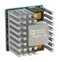


LTP8802A-1BIPV#PBF
DC/DC Converter, 45 to 65 V Input, 140 A, 500mV to 3.6 V Output, SMD, LTP8802A-1B Series
- Manufacturer: ANALOG DEVICES
- Product type: DC / DC Non Isolated Board Mount Converters - Adjustable Output
- SVHC: Lead (04-Feb-2026)
- Product Range: LTP8802A Series
- Output Current Max: 140A
- Output Voltage Max: 3.6V
| Delivery and price | |
|---|---|
| Units per pack | 1 |
| Price | 205.79 € |
| Current stock | 25+ |
| Lead time | 30 days |
LTP8802A-1B ## 54V, 140A DC/DC μModule Regulator with PMBus Interface ## **FEATURES** - n **High Efficiency at High Frequency** n **Up to 93.8% Efficiency at 813kHz, 54VIN to 3.3VOUT** - n **PMBus-Compliant I[2] C Serial Interface** - n **Monitor Voltage, Current, Temperature and Faults** - n **Internal EEPROM Fault Log Record** - n **Digitally Programmable Control Loop** - n **Program Voltage, Current Limits, Soft-Start/SoftStop, Frequency Synchronization and Phasing, Power-Good, Warnings, and Faults** - n **Wide Input Voltage Range: 45V to 65V** - n **Output Voltage Range: 0.5V to 3.6V** - n **Optimized for 45V to 65VIN to 3.3VOUT** - n **±0.5% Maximum DC Output Error with Differential Remote Voltage Sense** - n **±3% Current Readback Accuracy** - n Parallel and Current Share Multiple μModule ICs - n 22mm × 24mm × 22mm Surface-Mounted Package ## **APPLICATIONS** ## **DESCRIPTION** The LTP[®] 8802A-1B is a 140A step-down μModule[®] (micromodule) regulator that provides microprocessor core voltage from a 54V power distribution architecture. It features remote configurability and telemetry monitoring of power management parameters over PMBus, an open standard I[2] C-based digital interface protocol. The LTP8802A-1B is comprised of a programmable digital control system with precision mixed-signal circuitry, EEPROM, power MOSFETs, planar transformer, inductors, and supporting components. Its high level of integration minimizes component count and design time and maximizes flexibility and power density. The LTP8802A-1B preserves high efficiency at high conversion ratios by utilizing a quasi-resonant architecture that reduces high voltage switching losses. The LTP8802A-1B is available in a 22mm × 24mm × 22mm surface-mounted open frame package. All registered trademarks and trademarks are the property of their respective owners. - n High Current Distributed Power Systems - n Servers, Network, and Storage Equipment - n Intelligent Energy Efficient Power Regulation ## **TYPICAL APPLICATION** ## **3.3V, 140A Output DC/DC Module Regulator with PMBus Serial Interface** **==> picture [305 x 130] intentionally omitted <==** **----- Start of picture text -----**<br> 45V TO 65VVIN C14.7µF×2 VIN LTP8802A-1B VOUT 2.80k C3680µF V3.3V140AOUT<br>C2 ×10<br>7.0V 7V0 VS [+]<br>3.3V 3V3 100µF<br>ISHARE 100pF 499Ω ×8<br>7.5Ω<br>CTRL VS [–]<br>SMBALERT<br>PMBus<br>SDA<br>SCL<br>C1: GRM31CC72A475KE11L<br>OPTIONAL: SYNC C2: GRM32EE70J107ME15L<br>813kHz CLK<br>ADD GND C3: 6TPE680MI<br>WITH 50%<br>DUTY CYCLE 210Ω 8802a1b TA01a<br>**----- End of picture text -----**<br> ## **3.3VOUT Efficiency and Power Loss** **==> picture [152 x 141] intentionally omitted <==** **----- Start of picture text -----**<br> 95 45<br>92 40<br>EFFICIENCY<br>89 35<br>86 30<br>83 25<br>POWER LOSS<br>80 20<br>45V<br>77 54V 15<br>65V<br>74 10<br>7V0 AND 3V3 LOSSES INCLUDED<br>71 5<br>0 20 40 60 80 100 120 140<br>LOAD CURRENT (A)<br>8802a1b TA01b<br>EFFICIENCY (%) POWER LOSS (W)<br>**----- End of picture text -----**<br> Rev. A 1 For more information www.analog.com Document Feedback ## - LTP8802A 1B ## **ABSOLUTE MAXIMUM RATINGS** ## **PIN CONFIGURATION** ## **(Note 1)** VIN ............................................................. –0.3V to 70V 7V0 ..........................................................–0.3V to 7.75V 3V3, SYNC, CTRL, SMBALERT, SDA, SCL, ISHARE, ADD, VOUT .................................. –0.3V to 3.6V VS[+] .............................................................–0.3V to 1.6V VS[–] ............................................................ –0.3V to 0.3V Operating Junction Temperature Range LTP8802A-1B (Note 2, Note 3) ................... 0°C to 125°C Storage Temperature Range (Note 2) .....–40°C to 150°C Peak Solder Reflow Body Temperature ................. 245°C **==> picture [223 x 266] intentionally omitted <==** **----- Start of picture text -----**<br> TOP VIEW<br>SMBALERT SDA SCL GND VOUT VOUT VOUT<br>1 21 20 19 18 17 16<br>ISHARE 2<br>CTRL 3<br>15<br>ADD 4<br>GND<br>VS [+] 5<br>VS [–] 6<br>GND<br>14<br>VIN<br>22<br>7 8 9 10 11 12 13<br>SYNC 3V3 GND 7V0 VOUT VOUT VOUT<br>OPEN FRAME PACKAGE<br>22-PIN (22mm × 24mm × 22mm)<br>WEIGHT = 17.1g<br>**----- End of picture text -----**<br> ## **ORDER INFORMATION** |**LEAD FREE FINISH**|**PART MARKING**|**PACKAGE DESCRIPTION**|**MSL RATING**|**TEMPERATURE RANGE**| |---|---|---|---|---| |LTP8802A-1BIPV#PBF|LTP8802A-1B|22-Pin (22mm × 24mm) Open Frame|3|0°C to 125°C| Contact the factory for parts specified with wider operating temperature ranges. Rev. A 2 For more information www.analog.com - LTP8802A 1B ## **ELECTRICAL CHARACTERISTICS The** l **denotes the specifications which apply over the full operating temperature range, otherwise specifications are at TA = 25°C.** |**SYMBOL**|**PARAMETER**|**CONDITIONS**|**CONDITIONS**|**MIN**<br>**TYP**<br>**MAX**|**UNITS**| |---|---|---|---|---|---| |**VIN Supply**|||||| |VIN|Input Operating Range||l|45<br>65|V| |VIN(UVLO)|Input Undervoltage|VINRising||38<br>40<br>42|V| |||VINFalling||36<br>38<br>40|V| |VIN(OVLO)|Input Overvoltage|VINRising||67<br>70<br>73|V| |||VINFalling||65<br>68<br>71|V| |I(VIN)|No-Load Input Current, fSW= 813kHz|CTRL = 0V||0.1|mA| ||Input Supply Current, fSW= 813kHz|IOUT= 0A, VIN= 54V, VOUT= 3.3V||143|mA| |||IOUT= 20A, VIN= 54V, VOUT= 3.3V||1.36|A| |||IOUT= 100A, VIN= 54V, VOUT= 3.3V||6.50|A| |**7V0 Supply**|||||| |7V0|7V0 Operating Range||l|6.5<br>7<br>7.5|V| |7V0(UVLO)|7V0 Undervoltage|7V0 Rising|l|4.5|V| |||7V0 Falling|l|3.5|V| |I7V0|7V0 Input Current||l|0.39<br>0.46|A| |**3V3 Supply**|||||| |3V3|3V3 Operating Range||l|3.0<br>3.3<br>3.6|V| |3V3(UVLO)|3V3 Undervoltage|3V3 Rising|l|3.0|V| |||3V3 Falling|l|2.75|V| |I3V3|3V3 Input Current||l|60<br>70|mA| |**Output Specifications**|||||| |IOUT|Output Current Range||l|0<br>140|A| |IOUT(MAX)|Output Current Limit|||180|A| |VOUT|Regulated Output Voltage|IOUT= 0A, VIN= 54V, VOUTSet to 3.300V,<br>TJ= 25°C||3.283<br>3.300<br>3.316|V| |||IOUT= 0A, VIN= 54V, VOUTSet to 3.300V,<br>TJ= 0°C to 125°C|l|3.240<br>3.300<br>3.352|V| |VOUT(LOAD+LINE)|Line + Load Regulation|IOUT= 0A to 140A, VIN= 48V to 65V|l|3.234<br>3.300<br>3.366|V| |VOUT(AC)|VOUT(PK-PK)|VIN= 54V, VOUT= 3.3V,<br>COUT= 800μF MLCC, 6.8mF POSCAP||5.3|mV| ||VOUT(RMS)|VIN= 54V, VOUT= 3.3V,<br>COUT= 800μF MLCC, 6.8mF POSCAP||2.1|mV| |TSTART|Start Time|CTRL High to VOUT= 3.3V||3|ms| |TSTOP|Stop Time|CTRL Low to Output Disable||10|µs| |ΔVOUT(LS)|Maximum Output Voltage Excursion for<br>Dynamic Load Step|VIN= 54V, VOUT= 3.3V, COUT= 800μF<br>MLCC, 6.8mF POSCAP, ΔILOAD= 35A||60|mV| |TSETTLE|VOUTSettling Time to 1%|VIN= 54V, VOUT= 3.3V, COUT= 800μF<br>MLCC, 6.8mF POSCAP, ΔILOAD= 35A||30|µs| |Efficiency||VIN= 54V, VOUT= 3.3V, IOUT= 35A||90.1|%| |||VIN= 54V, VOUT= 3.3V, IOUT= 70A||93.5|%| |||VIN= 54V, VOUT= 3.3V, IOUT= 105A||93.8|%| |||VIN= 54V, VOUT= 3.3V, IOUT= 140A||92.6|%| Rev. A 3 For more information www.analog.com ## - LTP8802A 1B ## **ELECTRICAL CHARACTERISTICS The** l **denotes the specifications which apply over the full operating temperature range, otherwise specifications are at TA = 25°C.** |**SYMBOL**|**PARAMETER**|**CONDITIONS**|**CONDITIONS**|**MIN**<br>**TYP**<br>**MAX**|**UNITS**| |---|---|---|---|---|---| |**Oscillator**|||||| |fSW|Switching Frequency|Switching Frequency set to 813kHz|l|788<br>813<br>838|kHz| |fSYNC|SYNC Range||l|732<br>813<br>894|kHz| |**PMBus Monitoring**|||||| |IMON(OUT)|Output Current Monitor|VIN= 54V, VOUT= 3.3V, IOUT= 140A|l|±3|%| |IMON(IN)|Input Current Monitor|VIN= 54V, VOUT= 3.3V, IOUT= 140A|l|±5|%| |VOUTMON|Output Voltage Monitor|VIN= 54V, VOUT= 3.3V, IOUT= 0A,<br>TJ= 25°C||±0.5|%| |||VIN= 54V, VOUT= 3.3V, IOUT= 0A,<br>TJ= 0°C to 125°C|l|–1.5<br>+1.5|%| |VINMON|Input Voltage Monitor|VIN= 45V to 65V, VOUT= 3.3V, IOUT= 70A|l|±2|%| |TMON|Temp Monitor|VIN= 54V, VOUT= 3.3V, IOUT= 70A|l|±10|°C| |**Leakage Current Digital Inputs (CTRL, SDA, SCL, SYNC)**|||||| |IDGTL|Input Leakage Current|0V ≤ VPIN≤ 3.6V|l|10|µA| |**Control Section**|||||| |VSCM|VS Common Mode Range||l|–100<br>+100|mV| |VMRGN|Output Voltage Margin Range|||0.5<br>3.60|V| |VOUT(OVLO)|Output Overvoltage Protection|||4.0|V| |**Digital Inputs (CTRL, SDA, SCL, SYNC)**|||||| |VIH|Input High Threshold Voltage|V3V3= 3.3V|l|2.1|V| |VIL|Input Low Threshold Voltage|V3V3= 3.3V|l|0.8|V| |**Digital Outputs (SDA, SMBALERT)**|||||| |VOL|Output Low Voltage||l|0.6|V| |**PMBus Timing Characteristics (SDA, SCL)**|||||| |fSCL|Serial Bus Frequency||l|10<br>400|kHz| **Note 1:** Stresses beyond those listed under Absolute Maximum Ratings may cause permanent damage to the device. Exposure to any Absolute Maximum Rating condition for extended periods may affect device reliability and lifetime. **Note 3:** The LTP8802A-1BI includes overtemperature protection that is intended to protect the device during thermal overload conditions. Internal junction temperature may exceed 150°C if the overtemperature circuitry is active. **Note 2:** The LTP8802A-1BI is guaranteed over the full 0°C to 125°C operating junction temperature range. Operating lifetime is derated at junction temperatures greater than 125°C. Rev. A 4 For more information www.analog.com - LTP8802A 1B ## **TYPICAL PERFORMANCE CHARACTERISTICS** **==> picture [540 x 632] intentionally omitted <==** **----- Start of picture text -----**<br> Load Transient Response Load Transient Response Load Transient Response<br>105A to 140A Load Step 105A to 140A Load Step 105A to 140A Load Step<br>35A/ μ s 45VIN to 3.3VOUT 35A/ μ s 54VIN to 3.3VOUT 35A/ μ s 65VIN to 3.3VOUT<br>VOUT VOUT VOUT<br>AC-COUPLED AC-COUPLED AC-COUPLED<br>50mV/DIV 50mV/DIV 50mV/DIV<br>IOUT IOUT IOUT<br>100A/DIV 100A/DIV 100A/DIV<br>20µs/DIV 8802a1b G01 20µs/DIV 8802a1b G02 20µs/DIV 8802a1b G03<br>FIGURE 10 CIRCUIT FIGURE 10 CIRCUIT FIGURE 10 CIRCUIT<br>VIN = 45V, VOUT = 3.3V, fsw = 813kHz VIN = 54V, VOUT = 3.3V, fsw = 813kHz VIN = 65V, VOUT = 3.3V, fsw = 813kHz<br>COUT = 680µF ×10 POSCAP + 100µF ×8 CERAMIC COUT = 680µF ×10 POSCAP + 100µF ×8 CERAMIC COUT = 680µF ×10 POSCAP + 100µF ×8 CERAMIC<br>REG FE01h = 20, REG FE02h = 226, REG FE01h = 20, REG FE02h = 226, REG FE01h = 20, REG FE02h = 226,<br>REG FE03h = 180, REG FE04h = 70 REG FE03h = 180, REG FE04h = 70 REG FE03h = 180, REG FE04h = 70<br>Full Load Start-Up and Shut-Down No Load Start-Up and Shut-Down<br>Triggered by CTRL Triggered by CTRL<br>VOUT CTRL V OUT CTRL<br>500mV/DIV<br>VOUT V OUT<br>500mV/DIV<br>IOUT IOUT<br>50A/DIV<br>IIN IIN<br>100mA/DIV<br>IIN IIN<br>5A/DIV IOUT IOUT<br>50A/DIV<br>1ms/DIV 8802a1b G04 1ms/DIV 8802a1b G05<br>45VIN No Load VOUT Ripple 54VIN No Load VOUT Ripple 65VIN No Load VOUT Ripple<br>IOUT IOUT IOUT<br>100A/DIV 100A/DIV 100A/DIV<br>VOUT VOUT VOUT<br>AC-COUPLED AC-COUPLED AC-COUPLED<br>10mV/DIV 10mV/DIV 10mV/DIV<br>IIN IIN IIN<br>10A/DIV 10A/DIV 10A/DIV<br>500ns/DIV 8802a1b G06 500ns/DIV 8802a1b G07 500ns/DIV 8802a1b G08<br>FIGURE 10 CIRCUIT FIGURE 10 CIRCUIT FIGURE 10 CIRCUIT<br>VIN = 45V, VOUT = 3.3V, fSW = 813kHz VIN = 54V, VOUT = 3.3V, fSW = 813kHz VIN = 65V, VOUT = 3.3V, fSW = 813kHz<br>NO LOAD ON VOUT NO LOAD ON VOUT NO LOAD ON VOUT<br>Rev. A<br>**----- End of picture text -----**<br> 5 For more information www.analog.com ## - LTP8802A 1B ## **TYPICAL PERFORMANCE CHARACTERISTICS** **==> picture [523 x 610] intentionally omitted <==** **----- Start of picture text -----**<br> 45VIN Full Load VOUT Ripple 54VIN Full Load VOUT Ripple 65VIN Full Load VOUT Ripple<br>IOUT IOUT IOUT<br>100A/DIV 100A/DIV 100A/DIV<br>VOUT VOUT VOUT<br>AC-COUPLED AC-COUPLED AC-COUPLED<br>10mV/DIV 10mV/DIV 10mV/DIV<br>10A/DIVIIN 10A/DIVIIN 10A/DIVIIN<br>500ns/DIV 8802a1b G09 500ns/DIV 8802a1b G10 500ns/DIV 8802a1b G11<br>FIGURE 10 CIRCUIT FIGURE 10 CIRCUIT FIGURE 10 CIRCUIT<br>VIN = 45V, VOUT = 3.3V, fSW = 813kHz VIN = 54V, VOUT = 3.3V, fSW = 813kHz VIN = 65V, VOUT = 3.3V, fSW = 813kHz<br>140A LOAD ON VOUT 140A LOAD ON VOUT 140A LOAD ON VOUT<br>45VIN Overcurrent Protection 54VIN Overcurrent Protection 60VIN Overcurrent Protection<br>VIN 25V/DIVVIN 25V/DIVVIN<br>25V/DIV<br>VOUT VOUT VOUT<br>2V/DIV 2V/DIV 2V/DIV<br>IOUT IOUT IOUT<br>100A/DIV 100A/DIV 100A/DIV<br>IIN IIN IIN<br>20A/DIV 20A/DIV 20A/DIV<br>20ms/DIV 8802a1b G12 20ms/DIV 8802a1b G13 20ms/DIV 8802a1b G14<br>45VIN Short-Circuit Start-Up 54VIN Short-Circuit Start-Up 60VIN Short-Circuit Start-Up<br>VIN 25V/DIVVIN 25V/DIVVIN<br>25V/DIV<br>VOUT VOUT VOUT<br>1V/DIV 1V/DIV 1V/DIV<br>IOUT IOUT IOUT<br>250A/DIV 250A/DIV 250A/DIV<br>IIN IIN IIN<br>10A/DIV 10A/DIV 10A/DIV<br>250µs/DIV 8802a1b G15 250µs/DIV 8802a1b G16 250µs/DIV 8802a1b G17<br>Rev. A<br>**----- End of picture text -----**<br> 6 For more information www.analog.com - LTP8802A 1B ## **PIN FUNCTIONS** **SMBALERT (Pin 1):** Power-Good Output (Open-Drain). This pin is also used as the PMBus SMBALERT# signal. If unused, connect to GND. **ISHARE (Pin 2):** Analog Current Sharing Input and Output. This pin must connect to other μModule IC’s ISHARE pins for current sharing. If not used, this pin should be left floating. Do not load ISHARE with external circuitry. **CTRL (Pin 3):** Power Supply ON/OFF Input. This pin performs hardware on/off control. The factory default setting is to enable the LTP8802A-1B only when CTRL is logic-high (active-high), but can optionally be changed to active-low, or ignored, using register 0x02. If this pin is not used, connect to 3V3 if it is configured active-high, or GND if it is configured active-low or ignored. **ADD (Pin 4):** I[2] C/PMBus Address Select Input. Connect a resistor from ADD to GND. See the Applications Information section for more information about the PMBus address selection. **VS[+] (Pin 5):** Non-Inverting Voltage Sense Input. This pin functions as the Kelvin sense of VOUT at the load as well as the feedback point for the converter control loop. The VS[+] pin should be tied to a precision feedback resistor divider connected to the output voltage. The VS[+] pin requires 100pF capacitance to the VS[–] pin placed close to the LTP8802A-1B. The VS[+] feedback resistors need to have an equivalent parallel resistance < 2k. Otherwise, the control loop may be adversely affected. **VS[–] (Pin 6):** Inverting Voltage Sense Input. This pin functions as the Kelvin sense of GND at the load as well as the GND connection for the feedback point for the converter control loop. **SYNC (Pin 7):** Synchronization Input Signal. This pin is used as a reference for the internal oscillator and is referenced to GND. Synchronization is disabled by default. To enable synchronization, set 0xFE55[6] = 0 and then set 0xFE00 = 0b0100000 for the value to take effect. It is recommended that this input be disabled when not in use. To disable, set 0xFE55[6] = 1 and then set 0xFE00 = 0b0100000 for the value to take effect. To accomplish phase interleaving of multiple devices, a phase delay in steps of 22.5 degrees can be added using register 0x37[3:0]. **3V3 (Pin 8):** The 3V3 pin powers internal μModule circuitry. The typical 3V3 supply cur rent when operating is 60mA. The voltage on this pin must be within the specified operating range before the LTP8802A-1B can be enabled. **GND (Pins 9, 14, 15, 19):** μModule Ground. The GND pins carry high current and must be connected to large planes with sufficient internal layers. Be sure to keep the voltage at the pins roughly equal by taking care of the direction of current flow and debiasing of the ground planes. **7V0 (Pin 10):** The 7V0 pin powers internal μModule circuitry, including gate drivers. The typical 7V0 supply current when operating is 0.39A. The voltage on this pin must be within the specified operating range before the LTP8802A-1B can be enabled. **VOUT (Pins 11, 12, 13, 16, 17, 18):** The VOUT pins carry the high output current of the converter. As such, these pins must be connected to large power planes with sufficient internal layers. The PCB layout must be such that the two sets of VOUT pins see roughly the same voltage. This ensures high efficiency and balanced currents. Output voltage is digitally programmable from 0.5V to 3.6V. The VOUT pins are two rows of terminals and carry high steady-state output currents (from 0A up to 140A) and transient currents up to 180A. **SCL (Pin 20):** I[2] C/PMBus Serial Clock Input and Output (Open-Drain). **SDA (Pin 21):** I[2] C/PMBus Serial Data Input and Output (Open-Drain). **VIN (Pin 22):** The VIN pin supplies current to the primary power switches and operates from 54V/48V nominal inputs; for further details, see Absolute Maximum Ratings and Electrical Characteristics table for input voltage range. The LTP8802-1B requires, at minimum, a total of 10µF from low ESR ceramic bypass capacitors, located as close as possible to the VIN and GND pins. Two 4.7µF 1206/1210 X7* capacitors are recommended. Rev. A 7 For more information www.analog.com ## - LTP8802A 1B ## **APPLICATIONS INFORMATION** ## **COMPENSATION** The LTP8802A-1B offers programmable loop compensation to optimize the transient response without any hardware change. A Type 3 filter architecture has been implemented. To tailor the loop response to the specific application, the low frequency gain, zero location, pole location and high frequency gain can all be set individually. From the sensed voltage to the duty cycle, the transfer function of the filter in z-domain is resolved by Equation 1. **==> picture [240 x 57] intentionally omitted <==** Where: - A = filter pole register value (in decimal), 0xFE03. - B = filter zero register value (in decimal), 0xFE02. - C = high frequency gain register value (in decimal), 0xFE04. - D = low frequency gain register value (in decimal), 0xFE01. - LFG = 4.7744 × 10[7] /fSW. - HFG = 2.984 × 10[6] /fSW. As shown in Figure 1, adjusting low frequency gain register value changes the gain of the compensation over the low frequency range without moving the pole and zero locations. Adjusting high frequency gain register value changes the gain of the compensation over the high frequency range without moving the pole and zero locations. As shown in Figure 2, adjusting the pole and zero register values moves the double poles and double zeroes of the compensation. Increasing the filter zero and pole register values separates the double zeroes and double poles. It is recommended that LTpowerPlay **[®]** be used to program the filter. It is recommended that the user determines the appropriate value for the compensation registers using the LTpowerCAD[®] tool. An example of the bode plot of the typical application circuit with the recommended compensation settings is shown in Figure 3. Measured bode plot of the LTP8802A-1B in circuit Figure 9 with register setting (in decimal): 0xFE02 = 226, 0xFE03 = 180, 0xFE04 = 70, 0xFE01 = 8; crossover frequency: 22.0kHz, phase margin 101.7deg, gain margin 14.7dB. **==> picture [157 x 353] intentionally omitted <==** **----- Start of picture text -----**<br> 55<br>50<br>45<br>40 LG INCREASE<br>35<br>30<br>HG INCREASE<br>\ T 4 t<br>25<br>20 Neeee ae<br>15 rN ees ee<br>10<br>5<br>10 100 1k 10k 100k 1M<br>FREQUENCY (Hz)<br>8802a1b F01<br>Figure 1. Compensation Gain Adjustment<br>55<br>50<br>45<br>40<br>35<br>30 POLE<br>INCREASE<br>25<br>20<br>ZERO<br>15<br>INCREASE<br>10 | | Lr<br>5<br>10 100 1k 10k 100k 1M<br>FREQUENCY (Hz)<br>8802a1b F02<br>GAIN (dB)<br>GAIN (dB)<br>**----- End of picture text -----**<br> **Figure 1. Compensation Gain Adjustment** **Figure 2. Compensation Poles and Zeroes Adjustment** **Figure 3. Measured Bode Plot of the LTP8802A-1B** Rev. A 8 For more information www.analog.com - LTP8802A 1B ## **APPLICATIONS INFORMATION** ## **PolyPhase CONFIGURATION** When configuring a PolyPhase **[®]** rail with multiple LTP8802A-1B, share the SYNC and ISHARE pins, and provide an external clock source. The digital phase-locked loop is capable of determining the frequency on the SYNC pin and locking it to the internal oscillator. The lock or capture range is ±10% of the switching frequency (813kHz). The relative phasing can be configured in steps of 22.5 degrees, using register 0x37[3:0]. ## **PMBus COMMANDS AND LTpowerPlay** ## **PMBus Commands** There are multiple PMBus commands and manufacturerspecific commands, which can be customized to adjust the settings of LTP8802A-1B module, as listed in Table 1. These commands comply to the PMBus Power System Management Protocol. See the PMBus Communication and Command Processing section for details. ## **PolyPhase LOAD SHARING** Multiple LTP8802A-1B can be arrayed in order to provide a balanced load-share solution by connecting the ISHARE pins. Figure 4 illustrates a 2-phase design sharing connections required for load sharing. **==> picture [392 x 326] intentionally omitted <==** **----- Start of picture text -----**<br> 45V TOVIN C1 VIN VOUT VOUT = 3.3V, 280A<br>65V 4.7µF ×2 LTP8802A-1B C3 C4<br>5.62k 100µF 680µF<br>7.0V 7V0 VS [+] ×16 ×20<br>3.3V 3V3<br>1.00k<br>ISHARE 100pF<br>7.5Ω<br>CTRL<br>VS [–]<br>SMBALERT<br>PMBus<br>SDA<br>SCL<br>813kHz CLK SYNC<br>GND<br>WITH 50%<br>DUTY CYCLE ADD<br>210Ω<br>*CLOCK 0x37[3:0] = 0b0000<br>INTERLEAVING 0xFE55[6] = 0 (MUST SET 0xFE00 = 0b0100000<br>CONFIGURED FOR VALUE TO TAKE EFFECT)<br>THROUGH<br>PMBus 45V TOVIN C2 VIN VOUT<br>65V 4.7µF ×2 LTP8802A-1B<br>5.62k<br>7.0V 7V0 VS [+]<br>3.3V 3V3<br>1.00k<br>ISHARE 100pF<br>CTRL 7.5Ω<br>VS [–]<br>SMBALERT<br>PMBus<br>SDA<br>SCL<br>C1, C2: GRM31CC72A475KE11L<br>SYNC C3: GRM32EE70J107ME15L<br>GND<br>C4: 6TPE680MI<br>ADD<br>750Ω 8802a1b F04<br>0x37[3:0] = 0b0100<br>0xFE55[6] = 0 (MUST SET 0xFE00 = 0b0100000<br>FOR VALUE TO TAKE EFFECT)<br>**----- End of picture text -----**<br> **Figure 4. 2-Phase Operation Producing 3.3V at 280A** Rev. A 9 For more information www.analog.com - LTP8802A 1B ## **APPLICATIONS INFORMATION** ## **Table 1. LTP8802A-1B Summary of Customizable Commands and Features** |**PMBus COMMAND NAME**<br>**OR FEATURE**|**CMD CODE**<br>**REGISTER**|**COMMAND OR FEATURE**<br>**DESCRIPTION**|**TYPE**|**DATA**<br>**UNITS**|**DATA**<br>**FORMAT**|**NVM**<br>**ATTRIBUTES**| |---|---|---|---|---|---|---| |WRITE_PROTECT|0x10|Protect the PMBus device against accidental writes.|R/W Byte|NA|Bit Field|Stored in user-<br>editable NVM.| |VIN_ON|0x35|Sets the value of the input voltage (VRMS) at which<br>the device starts power conversion.|R/W Word|Volts|Linear<br>11|Stored in user-<br>editable NVM.| |VIN_OFF|0x36|Sets the value of the input voltage (VRMS) at which<br>the device stops power conversion.|R/W word|Volts|Linear<br>11|Stored in user-<br>editable NVM.| |VIN_OV_FAULT_LIMIT|0x55|Sets the upper voltage threshold (in volts) measured<br>at the sense/input pin that causes an overvoltage<br>fault condition.|R/W Word|Volts|Linear<br>11|Stored in user-<br>editable NVM.| |VIN_UV_FAULT_LIMIT|0x59|Sets the lower voltage threshold (in volts) measured<br>at the sense/input pin that causes an undervoltage<br>fault condition.|R/W Word|Volts|Linear<br>11|Stored in user-<br>editable NVM.| |IIN_OC_FAULT_LIMIT|0x5B|Sets the threshold value (in amperes) measured at<br>the sense/input pin that causes an overcurrent fault<br>condition.|R/W Word|Amps|Linear<br>11|Stored in user-<br>editable NVM.| |POUT_OP_FAULT_LIMIT|0x68|Sets the upper power threshold (in watts) measured<br>at the sense/output pin that causes an output<br>overpower fault condition.|R/W Word|Watts|Linear<br>11|Stored in user-<br>editable NVM.| |NM_DIGFILT_LF_GAIN_SETTING|0xFE01|Determines the low frequency gain of the loop<br>response in normal mode.|R/W Byte|NA|NA|Stored in user-<br>editable NVM.| |NM_DIGFILT_ZERO_SETTING|0xFE02|Determines the position of the final zero in<br>normal mode.|R/W Byte|NA|NA|Stored in user-<br>editable NVM.| |NM_DIGFILT_POLE_SETTING|0xFE03|Determines the position of the final pole in<br>normal mode.|R/W Byte|NA|NA|Stored in user-<br>editable NVM.| |NM_DIGFILT_HF_GAIN_SETTING|0xFE04|Determines the high frequency gain of the loop<br>response in normal mode.|R/W Byte|NA|NA|Stored in user-<br>editable NVM.| Rev. A 10 For more information www.analog.com - LTP8802A 1B ## **APPLICATIONS INFORMATION** ## **LTpowerPlay: AN INTERACTIVE GUI FOR DIGITAL POWER MODULES** The LTpowerPlay is a powerful graphical user interface (GUI) that supports the digital power module LTP8802A-1B, as shown in Figure 5. In online mode, LTpowerPlay can be used to evaluate single or multiple LTP8802A-1B power modules of different types by connecting to a demo board or the user application. In offline mode with no hardware connected via PMBus, LTpowerPlay can also be used to build the project file with configuration of multiple modules, and the project file can be saved and reloaded later. Moreover, during board bringup, LTpowerPlay can be used as a valuable diagnostic tool to program the power system, to tweak the system settings, or to diagnose system issues. The LTpowerPlay utilizes Analog Device’s USB-to-I[2] C/ SMBus/PMBus Controller, DC1613A, to communicate with circuit boards including the DC3190B-F (single LTP8802A-1B module) demo board or a customer target system. Further context information, including tutorial demos, is available here. **Figure 5. LTpowerPlay Main Interface** **==> picture [18 x 6] intentionally omitted <==** **----- Start of picture text -----**<br> Rev. A<br>**----- End of picture text -----**<br> 11 For more information www.analog.com - LTP8802A 1B ## **APPLICATIONS INFORMATION** ## **PMBus COMMUNICATION AND COMMAND PROCESSING** The LTP8802A-1B series communicate through PMBus with other compliant devices. The LTP8802A-1B is always configured as a subordinate device in the overall system, requiring a two-wire interface with one data pin (SDA) and one clock pin (SCL). As subordinate devices, LTP8802A-1B power modules decode the command sent from the main device and respond accordingly. Data transfer of the PMBus subordinate is based on PMBus commands. According to the PMBus/SMBus/I[2] C communication protocol, all PMBus commands start with a subordinate address with the R/W bit cleared (set to 0), followed by the command code, with mostly the stop bit as the last bit in a complete data transfer. Commands can be categorized as send, read, or write types. For read or write commands, data is transferred between devices in a byte wide format. For send commands, the subordinate device execute the commands upon receiving the stop bit. To ensure robust communication, the main and subordinate devices send acknowledge (ACK) or no acknowledge (NACK) bits as a method of handshaking, eliminating the busy errors between devices. Manufacturer-specific extended commands are also supported by LTP8802A-1B. These commands follow the same protocol as the standard PMBus commands. However, the command code consists of two bytes: Command code extension (0xFE) and Extended command code (0x00 to 0xFF). By use of the manufacturer-specific extended commands, the PMBus command set is greatly extended. ## **PMBus ADDRESS SELECTION** The PMBus address is set by connecting an external resistor from the ADD pin to GND. Table 2 lists the recommended resistor values and associated PMBus addresses. **Table 2. Recommended Resistor Values and Associated PMBus Addresses** |**PMBus Addresses**|| |---|---| |**PMBus ADDRESS**|**1% RESISTOR ON ADD PIN (Ω)**| |0x40|210(or Connect to GND)| |0x41|750| |0x42|1330| |0x43|2050| |0x44|2670| |0x45|3570| |0x46|4420| |0x47|5360| |0x48|6340| |0x49|7320| |0x4A|8450| |0x4B|9530| |0x4C|10,700| |0x4D|12,100| |0x4E|13,700| |0x4F|15,000(or Connect to 3V3)| Rev. A 12 For more information www.analog.com - LTP8802A 1B ## **APPLICATIONS INFORMATION** **==> picture [523 x 582] intentionally omitted <==** **----- Start of picture text -----**<br> 155 155<br>140 140<br>125 125<br>110 110<br>95 95<br>80 200LFM (1.02m/s) 80 200LFM (1.02m/s)<br>400LFM (2.03m/s) 400LFM (2.03m/s)<br>65 500LFM (2.54m/s) 65 500LFM (2.54m/s)<br>VIN = 48V VIN = 54V<br>50 VOUT = 3.3V 50 VOUT = 3.3V<br>fSW = 813kHz fSW = 813kHz<br>35 220mm × 230mm 35 220mm × 230mm<br>8-LAYER PCB 8-LAYER PCB<br>20 20<br>0 20 40 60 80 100 120 0 20 40 60 80 100 120<br>TEMPERATURE (°C) TEMPERATURE (°C)<br>8802a1b G06 8802a1b G07<br>Figure 6. Thermal Derating Figure 7. Thermal Derating<br>48VIN, 3.3VOUT, 813kHz 54VIN, 3.3VOUT, 813kHz<br>GND<br>VOUT<br>VOUT<br>VIN<br>+<br>+<br>GND GND<br>VOUT<br>VOUT<br>GND<br>88002a1b F08a 8802a1b F08b<br>(a) Top Layer (a) Bottom Layer<br>LOAD CURRENT (A) LOAD CURRENT (A)<br>+<br>+<br>**----- End of picture text -----**<br> **Figure 8. Recommended PCB Layout, Top View** **==> picture [18 x 6] intentionally omitted <==** **----- Start of picture text -----**<br> Rev. A<br>**----- End of picture text -----**<br> 13 For more information www.analog.com - LTP8802A 1B ## **TYPICAL APPLICATION** **==> picture [350 x 147] intentionally omitted <==** **----- Start of picture text -----**<br> 45V TO 65VVIN C14.7µF ×2 VIN LTP8802A-1B VOUT 2.00k C3680µF V2.5V140AOUT<br>C2 ×10<br>7.0V 7V0 VS [+]<br>100µF<br>3.3V 3V3ISHARE 100pF 499Ω ×8<br>7.5Ω<br>CTRL VS [–]<br>SMBALERT<br>PMBus<br>SDA<br>SCL<br>C1: GRM31CC72A475KE11L<br>OPTIONAL: SYNC C2: GRM32EE70J107ME15L<br>813kHz CLK C3: 6TPE680MI<br>WITH 50% ADD GND<br>DUTY CYCLE 210Ω 8802a1b F09<br>**----- End of picture text -----**<br> **Figure 9. 2.5V 140A 813kHz Step-Down Module with PMBus** Rev. A 14 For more information www.analog.com - LTP8802A 1B ## **TYPICAL APPLICATION** **==> picture [338 x 143] intentionally omitted <==** **----- Start of picture text -----**<br> 45V TO 65VVIN C14.7µF×2 VIN LTP8802A-1B VOUT 2.80k C2 C3680µF×10 V3.3V140AOUT<br>7.0V 7V0 VS [+] 100µF<br>3.3V 3V3 ×8<br>ISHARE 100pF 499Ω<br>7.5Ω<br>CTRL VS [–]<br>SMBALERT<br>PMBus<br>SDA<br>SCL C1: GRM31CC72A475KE11L<br>C2: GRM32EE70J107ME15L<br>OPTIONAL: SYNC<br>C3: 6TPE680MI<br>813kHz CLK<br>WITH 50% ADD GND<br>DUTY CYCLE 210Ω 8802a1b F10<br>**----- End of picture text -----**<br> **Figure 10. 3.3V 140A 813kHz Step-Down Module with PMBus** **==> picture [18 x 6] intentionally omitted <==** **----- Start of picture text -----**<br> Rev. A<br>**----- End of picture text -----**<br> 15 For more information www.analog.com - LTP8802A 1B ## **TYPICAL APPLICATION** **==> picture [498 x 349] intentionally omitted <==** **----- Start of picture text -----**<br> VOUT = 3.3V, 280A<br>45V TO VIN C1 VIN VOUT<br>LTP8802A-1B<br>65V 4.7µF ×2<br>7.0V 7V0 C3 C4<br>5.62k 10µF 680µF<br>3.3V 3V3 6.81k ×16 ×20<br>ISHARE VS [+] TRIM [+]<br>CTRL<br>100pF<br>SMBALERT 1.00k<br>PMBus 7.5Ω TRIM [–]<br>SDA VS [–]<br>SCL<br>813kHz CLK SYNC<br>WITH 50% ADD GND<br>DUTY CYCLE<br>210Ω<br>0x37[3:0] = 0b0000<br>*CLOCK<br>INTERLEAVING 0xFE55[6] = 0 (MUST SET 0xFE00 = 0b0100000 C1, C2: GRM31CC72A475KE11L<br>CONFIGURED FOR VALUE TO TAKE EFFECT) C3: GRM32EE70J107ME15L<br>THROUGHPMBus 45V TO VIN C2 VIN VOUT C4: 6TPE680MI<br>65V 4.7µF ×2 LTP8802A-1B CONNECT TRIMOR SIMILAR POWER SYSTEM MANAGER [+] AND TRIM [–] TO LTC2979<br>7.0V 7V0<br>3.3V 3V3 5.62k<br>ISHARE 6.81k<br>VS [+] TRIM [+]<br>CTRL<br>SMBALERT 100pF 1.00k<br>PMBus SDA 7.5Ω TRIM [–]<br>VS [–]<br>SCL<br>SYNC<br>ADD GND<br>750Ω 8802A1b F11<br>0x37[3:0] = 0b0100<br>0xFE55[6] = 0 (MUST SET 0xFE00 = 0b0100000<br>FOR VALUE TO TAKE EFFECT)<br>**----- End of picture text -----**<br> **Figure 11. 2-Phase Operation Producing 3.3V at 280A with Power System Management Features** Rev. A 16 For more information www.analog.com - LTP8802A 1B ## **PACKAGE DESCRIPTION** **==> picture [500 x 610] intentionally omitted <==** **----- Start of picture text -----**<br> DETAIL B DETAIL C 14 15<br>13<br>16<br>e2<br>12<br>17<br>11 18<br>10 DETAIL D LTPXXXX<br>19<br>9 PACKAGE BOTTOM VIEW<br>8 20 e1<br>21 PACKAGE PIN LABELING MAY VARY AMONG PRODUCTS. REVIEW EACH PACKAGE LAYOUT CAREFULLY PACKAGE IN TRAY LOADING ORIENTATION<br>7 1<br>!<br>22 6 5 4 3 2 5 NOTES: 1. DIMENSIONING AND TOLERANCING PER ASME Y14.5M-1994 2. ALL DIMENSIONS ARE IN MILLIMETERS 3. PRIMARY DATUM -Z- IS SEATING PLANE DETAILS OF PIN 1 IDENTIFIER ARE OPTIONAL,4 BUT MUST BE LOCATED WITHIN THE ZONE INDICATED. THE PIN 1 IDENTIFIER MAY BE EITHER A MOLD OR MARKED FEATURE 5 COMPONENT PIN 1 TRAY PIN 1 BEVEL<br>DETAIL A SEE NOTES<br>ccc Z // ddd Z Z<br>H ccc Z<br>H1<br>NOTES PCB THK<br>H2<br>MAX 22.50 2.10 2.03 0.20 0.40 0.20 0.35<br>H DIMENSIONS NOM 24.00 22.00 22.00 1.90 1.88 2.00 3.65<br>SIDE VIEWS<br>(PC-22-1)<br>MIN 21.50 1.70 1.73<br>TOTAL NUMBER OF INTERCONNECTS: 22<br> 22mm × 24mm × 22mm<br>D E H H1 H2 e1 e2 aaa bbb ccc ddd<br>SYMBOL<br>H1<br>H2<br>22-Terminal Printed Circuit Assembly [PCA]<br>aaa Y 5.75 REF PIN 1 CORNER 4 0.000<br>2×<br>D Y 10.800 8.100 5.495 0.650 2.650 4.650 6.650 8.650 10.800<br>X<br>E<br>20.50 REF TOP VIEW<br>11.50 REF<br>6.25 REF 11.50 REF 6.25 REF SUGGESTED PCB LAYOUT<br>PACKAGE TOP VIEW WITH SINK<br>0.25±0.15 22.50 REF 4.75 REF 10.875 5.495 0.000 5.495 10.875<br>10-23-2023-Ø<br>Z<br>10.050 10.050<br>9.875<br>8.050<br>7.375<br>6.050<br>5.375<br>4.050<br>2.900<br>0.000 0.000<br>0.650 0.625<br>4.265<br>4.275 4.250<br>4.265<br>7.925 7.900<br>aaa X 2×<br>PKG-007867<br>**----- End of picture text -----**<br> **==> picture [18 x 6] intentionally omitted <==** **----- Start of picture text -----**<br> Rev. A<br>**----- End of picture text -----**<br> 17 For more information www.analog.com - LTP8802A 1B ## **PACKAGE DESCRIPTION** ## **22-Terminal Printed Circuit Assembly [PCA] 22mm × 24mm × 22mm** **(PC-22-1)** **==> picture [427 x 458] intentionally omitted <==** **----- Start of picture text -----**<br> 1.60±0.10<br>14× bbb Z X Y<br>1.00±0.10<br>DETAIL A<br>2.40±0.10<br>6× bbb Z X Y<br>1.50±0.10<br>DETAIL B DETAIL D<br>10.00±0.30<br>2× bbb Z X Y<br>2.50±0.30<br>DETAIL C<br>bbb Z X Y<br>14×<br>bbb Z X Y<br>6×<br>0.000 25 0.6 50 4.2 65 4.2<br>bbb Z X Y<br>2×<br>**----- End of picture text -----**<br> Rev. A 18 For more information www.analog.com - LTP8802A 1B ## **REVISION HISTORY** |**REV**|**DATE**|**DESCRIPTION**|**PAGE NUMBER**| |---|---|---|---| |0|11/23|Initial Release.|—| |A|05/24|Updated URL to the link here.<br>Updated units in Figure 6 and Figure 7.|11<br>13| Rev. A 19 Information furnished by Analog Devices is believed to be accurate and reliable. However, no responsibility is assumed by Analog Devices for its use, nor for any infringements of patents or other rights of third parties that may result from its use. Specifications subject to change without notice. No license is granted by implicatiFor more informati **on** or otherwise under any patent or patent rights of Analog Devices.www.analog.com - LTP8802A 1B ## **PACKAGE PHOTOS** ## **Part marking is either ink mark or laser mark** ## **DESIGN RESOURCES** |**DESIGN RESOURCES**||| |---|---|---| |**SUBJECT**|**DESCRIPTION**|| |µModule Design and Manufacturing Resources|Design:<br>• Selector Guides<br>• Demo Boards and Gerber Files<br>• Free Simulation Tools|Manufacturing:<br>• Quick Start Guide<br>• PCB Design, Assembly and Manufacturing Guidelines<br>• Package and Board Level Reliability| |µModule Regulator Products Search|1. Sort table of products by parameters and download the result as a spread sheet.<br>2. Search using the Quick Power Search parametric table.<br>INPUT |<br>Vin(Min)<br>Vv<br>Vin(Max)<br>Vv<br>OUTPUT |<br>Vout<br>Vv<br>Jout<br>A<br>FEATURES |<br>Low EMI<br>Ultrathin<br>Internal Heat Sink|| |Digital Power System Management|Analog Devices’ family of digital power supply management ICs are highly integrated solutions that<br>offer essential functions, including power supply monitoring, supervision, margining and sequencing,<br>and feature EEPROM for storing user configurations and fault logging.|| ## **RELATED PARTS** |**PART NUMBER **|**DESCRIPTION**|**COMMENTS**| |---|---|---| |LTP8800-1A|54VIN, 150A Module Regulator with Digital Power<br>System Management, Optimized for 0.8VOUT|45V ≤ VIN≤ 65V, 0.5V ≤ VOUT≤ 1.1V, PMBus with Control and Telemetry, ±0.5% of<br>Maximum DC Output Error, 22mm × 24mm × 6.7mm Surface-Mount Package| |LTP8800-4A|54VIN, 200A Module Regulator with Digital Power<br>System Management, Optimized for 0.8VOUT|45V ≤ VIN≤ 65V, 0.5V ≤ VOUT≤ 1.1V, PMBus with Control and Telemetry, ±0.5% of<br>Maximum DC Output Error, 22mm × 24mm × 22mm Surface-Mount Package| |LTP8803-1A|54VIN, 160A Module Regulator with Digital Power<br>System Management, Optimized for 1.2VOUT|45V ≤ VIN≤ 65V, 0.5V ≤ VOUT≤ 1.5V, PMBus with Control and Telemetry, ±0.5% of<br>Maximum DC Output Error, 22mm × 24mm × 22mm Surface-Mount Package| |LTM<br>®4664A|54VIN, Dual 30A or Single 60A µModule Regulator<br>with Digital Power System Management|30V ≤ VIN≤ 58V, 0.5V ≤ VOUT≤ 1.2V, PMBus with Control and Telemetry, ±0.5% of<br>Maximum DC Output Error, 16mm × 16mm × 7.72mm BGA Package| |LTM4700|Dual 50A or Single 100A µModule Regulator with<br>Digital Power System Management|4.5V ≤ VIN≤ 16V, 0.5V ≤ VOUT≤ 1.8V, PMBus with Control and Telemetry, ±0.5% of<br>Maximum DC Output Error, 15mm × 22mm × 7.87mm BGA Package| |LTM4681|Quad 31.25A or Single 125A µModule Regulator<br>with Digital Power System Management|4.5V ≤ VIN≤ 16V, 0.5V ≤ VOUT≤ 3.3V, PMBus with Control and Telemetry, ±0.5% of<br>Maximum DC Output Error, 15mm × 22mm × 8.17mm BGA Package| |LTM4660|60V, 300W Nonisolated µModule Bus Converter|30V ≤ VIN≤ 60V, 7.5V ≤ VOUT≤ 18V, Up to 300W, 16mm × 16mm × 10.34 BGA Package| Rev. A 05/24 www.analog.com 20 ANALOG DEVICES, INC. 2023-2024 For more information www.analog.com
Updated at April 10, 2026
Since its inception in 1965, Analog Devices has established itself as a global leader in the design and manufacturing of high-performance analog, mixed-signal, and digital signal processing (DSP) integrated circuits. The company is renowned for solving complex engineering challenges by providing critical technologies that seamlessly convert real-world phenomena into precise electrical signals for the industrial, automotive, communications, and consumer markets. Within its extensive portfolio, Analog Devices provides highly reliable clock, timing, and frequency management solutions, featuring a comprehensive array of precision timers, oscillators, and pulse generators. Complementing this core lineup is a robust offering of driver and interface ICs, particularly high-performance I/O expanders that enable seamless connectivity and streamline complex electronic system architectures. Beyond these foundational integrated circuits, Analog Devices leads the industry in sensor innovation, delivering advanced MEMS accelerometers and integrated MEMS modules designed for exceptional precision in motion sensing. To support complete hardware designs, the company's specialized offerings also encompass discrete bipolar transistors, sub-2.4GHz RF transceivers, temperature-compensated oscillators, and dedicated power management components such as DC/DC converters and LED driver ICs.
About Novapart
Novapart is a B2B electronic component broker specialising in stock shortages and cost reduction. We source hard-to-find parts and identify compliant alternatives across a catalogue of 410,000+ components from 500+ manufacturers.
Learn more →Stock Shortage Specialist
When a component is unavailable, discontinued or has an unacceptable lead time, we tap into our network of vetted European and Asian distributors to source what you need — without compromising on quality or traceability.
Request a quote →Compliant Alternatives
We identify pin-to-pin, electrically equivalent substitutes that meet the same certifications (RoHS, AEC-Q100, REACH) as your original specification — validated against datasheets, not just part numbers. Often at a lower cost.
BOM Analysis service →