
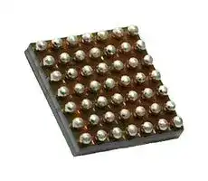


LTM4702EY#PBF
DC/DC POL Converter, Adjustable, Buck (Step Down), 3 V to 16 V in, 0.3 V to 5.7 V /8 A, 3MHz, BGA-49
- Manufacturer: ANALOG DEVICES
- Product type: DC / DC Non Isolated Board Mount Converters - Adjustable Output
- SVHC: No SVHC (04-Feb-2026)
- Depth: 6.25mm
- Width: 6.25mm
- Height: 5.07mm
- Topology: Buck (Step Down)
- No. of Pins: 49Pins
- Product Range: LTM4702 Series
- No. of Outputs: 1 Output
- Output Current: 8A
- Output Power Max: -
- Input Voltage Max: 16V
- Input Voltage Min: 3V
- Output Current Max: 8A
- Output Voltage Max: 5.7V
- Output Voltage Min: 300mV
- Switching Frequency: 3MHz
- Input Voltage DC Max: 16V
- Input Voltage DC Min: 3V
- DC / DC Converter Type: BGA-49, Micro Module
- DC / DC Converter IC Case: BGA
- Operating Temperature Max: 125°C
- Power Supply Applications: ITE & Industrial
- DC / DC Converter Output Type: Adjustable
| Delivery and price | |
|---|---|
| Units per pack | 520 |
| Price | 12.6 € |
| Current stock | 10+ |
| Lead time | 30 days |
LTM4702 ## 16VIN, 8A Ultralow Noise Silent Switcher µModule Regulator ## **FEATURES** - n **Complete Solution in <1cm[2] (Single-Sided PCB) or 0.5cm[2] (Dual-Sided PCB)** - n **Low Noise Silent Switcher Architecture** - n **Ultralow EMI Emissions** - n **Ultralow RMS Noise (10Hz to 100kHz): 8μVRMS** - n **±1.5% Maximum Total DC Output Voltage Error Over Line, Load, and Temperature** - n Input Voltage Range: 3V to 16V - n Output Voltage Range: 0.3V to 5.7V - n 8A Maximum Continuous Output Current - n Adjustable and Synchronizable: 300kHz to 3MHz - n Current Mode Control, Fast Transient Response - n Forced Continuous Mode Capability - n Multiphase Parallel with Current Sharing - n Programmable Power Good - n 6.25mm × 6.25mm × 5.07mm BGA Package ## **APPLICATIONS** - n Telecom, Networking, and Industrial Equipment - n RF Power Supplies: PLLs, VCOs, Mixers, LNAs, PAs - n Low Noise Instrumentation - n High Speed/High Precision Data Converters ## **DESCRIPTION** The LTM[®] 4702 is a complete 8A step-down Silent Switcher[®] µModule[®] regulator in a tiny 6.25mm × 6.25mm × 5.07mm BGA package. Included in the package are the switching controller, the power MOSFETs, an inductor, and support components. Operating over an input voltage range of 3V to 16V, the LTM4702 supports an output range of 0.3V to 5.7V. A single resistor sets the output voltage, providing unity gain operation over the output range and resulting in virtually constant output noise independent of the output voltage. Only bulk input and output capacitors are needed to finish the design. The LTM4702 employs Silent Switcher architecture with internal hot loop bypass capacitors to achieve both low EMI and high efficiency. Also, the LTM4702 has an ultralow noise architecture to obtain exceptional low-frequency (<100kHz) output noise. These low EMI and low noise features make the LTM4702 ideal for high current and noise-sensitive applications, which benefit from the high efficiency of a synchronous switching regulator. The LTM4702 is available with RoHS compliant terminal finish. All registered trademarks and trademarks are the property of their respective owners. ## **TYPICAL APPLICATION** **==> picture [486 x 173] intentionally omitted <==** **----- Start of picture text -----**<br> 3V to 16V Input to 1V, 8A Output Efficiency, VIN = 12V<br>100<br>VOUT<br>VIN VIN VOUT 1V 95<br>3V TO 16V 10µF SVIN VOSNS 8A 90<br>RUN 49.9k 100µF<br>×2<br>85<br>COMPa LTM4702 PGSET<br>COMPb 80<br>SET GND<br>75<br>RT 1.0VOUT AT 800kHz<br>AGND 70 1.5V OUT AT 1.2MHz<br>4.7µF 10k 137k 4702 TA01a 2.5VOUT AT 1.4MHz<br>65 3.3V OUT AT 1.7MHz<br>5.0VOUT AT 1.9MHz<br>60<br>0.0 1.0 2.0 3.0 4.0 5.0 6.0 7.0 8.0<br>LOAD CURRENT (A)<br>4702 TA01b<br>EFFICIENCY (%)<br>**----- End of picture text -----**<br> Rev. 0 1 For more information www.analog.com Document Feedback ## LTM4702 ## **ABSOLUTE MAXIMUM RATINGS** ## **(Notes 1, 2)** VIN, SVIN, RUN, PG ...................................................18V SYNC, VOUT, VOSNS, SET, PGSET ................................6V PHMODE, COMPa, RT .................................................4V TSENSE[+] to TSENSE[−] (Current) ...................................5mA Internal Operating Junction Temperature Range E-Grade, I-Grade .................................. –40° to 125°C Storage Temperature Range .....................–55° to 125°C Peak Solder Reflow Body Temperature .................250°C ## **PIN CONFIGURATION** **==> picture [191 x 251] intentionally omitted <==** **----- Start of picture text -----**<br> TOP VIEW<br>1 2 3 4 5 6 7<br>A VOUT<br>BANK 1 SVIN VIN BANK 4<br>B<br>TSENSE [+] TSENSE [–]<br>C<br>RUN COMPa COMPb<br>BANK 3<br>D<br>RT AGND INTVCC GND<br>E<br>SET PGSET PHMODE<br>F<br>VOSNS PG BANK 2 SW CLKOUT<br>G VOUT<br>SYNC GND<br>BGA PACKAGE<br>49-PIN (6.25mm × 6.25mm × 5.07mm)<br>TJMAX = 125°C, θJA = 20°C/W, θJCtop = 31°C/W,<br>θJCbottom = 13.3°C/W, WEIGHT = 0.7g<br>**----- End of picture text -----**<br> NOTES: 1. θ VALUES ARE DETERMINED BY SIMULATION PER JESD-51 CONDITIONS. 2. θ JA VALUE IS OBTAINED WITH DEMO BOARD. 3. SEE THE TYPICAL PERFORMANCE CHARACTERISTICS SECTION FOR LAB MEASUREMENT AND DERATING CURVES. ## **ORDER INFORMATION** |**PART NUMBER**|**PAD OR BALL FINISH**|**PART MARKING**|**PART MARKING**|**PACKAGE TYPE**|**MSL RATING**|**TEMPERATURE RANGE**<br>**(SEE NOTE 2)**| |---|---|---|---|---|---|---| |||**DEVICE**|**FINISH CODE**|||| |LTM4702EY#PBF|SAC305(RoHS)|4702|e1|BGA|4|–40°C to 125°C| |LTM4702IY#PBF|SAC305(RoHS)|4702|e1|BGA|4|–40°C to 125°C| - Contact the factory for parts specified with wider operating temperature ranges. Pad or ball finish code is per IPC/JEDEC J-STD-609. - Recommended LGA and BGA PCB Assembly and Manufacturing Procedures - LGA and BGA Package and Tray Drawings Rev. 0 2 For more information www.analog.com LTM4702 **ELECTRICAL CHARACTERISTICS The** l **denotes the specifications that apply over the specified internal operating junction temperature range (Note 2), otherwise specifications are at TA = 25°C, VIN = 12V, per the typical application (Note 5).** |**SYMBOL**|**PARAMETER**|**CONDITIONS**|**CONDITIONS**|**MIN**<br>**TYP**<br>**MAX**|**UNITS**| |---|---|---|---|---|---| |VIN|Power Input DC Voltage||l|3<br>16|V| |SVIN|Signal Input DC Voltage(Note 8)||l|3<br>16|V| |VOUT(RANGE)|Output Voltage Range|VPGSET= 0.5V|l|0.3<br>5.7|V| |VOUT(DC)|Output Voltage, Total Variation with<br>Line and Load|CIN= 10μF, COUT= 200μF Ceramic,<br>RSET= 10k, FCM,<br>VIN= 3V to 16V, SVIN= 6V, IOUT= 100mA to 8A|l|0.985<br>1<br>1.015|V| |ISET|SET Pin Current|VIN= SVIN= 6V, RSET= 10k, IOUT= 100mA||99.5<br>100<br>100.5|μA| |ISET_START|Fast Start-Up Set Pin Current|VIN= SVIN= 6V, VSET= 1V, VPGSET= 0V||2<br>2.5<br>3|mA| |tSTART|Start-Up Time (Notes 3, 9)|VOUT= 1V, CSET= 1μF, VPGSET= 0.5V<br>VOUT= 1V, CSET= 4.7μF, VPGSET= 0.5V<br>VOUT= 1V, CSET= 1μF, RPGSET= 49.9k,<br>VOUT= 1V, CSET= 4.7μF, RPGSET= 49.9k||25<br>120<br>1<br>2.5|ms<br>ms<br>ms<br>ms| |VRUN|RUN Pin ON Threshold|VRUNRising||1.32<br>1.37|V| ||RUN Pin Hysteresis|||50|mV| |VINTVCC|Internal VCCVoltage|||3.2<br>3.4<br>3.6|V| |IQ_SVIN|SVINQuiescent Current|SVIN= 12V, VRUN= 0V, Shutdown<br>SVIN= 12V, RT= 47k, FCM||50<br>13<br>17|μA<br>mA| |VOUT_SPOTNOISE|Output Noise Spectral Density (2kHz)<br>(Notes 3, 4, 6, 7)|SVIN= 12V, VOUT= 1V, COUT= 200µF, RSET= 10k,<br>CSET= 4.7µF, fSW= 2MHz||4|nV/√Hz| |VOUT_RMSNOISE|Output RMS Noise (10Hz to 100kHz)<br>(Notes 3, 4, 6, 7)|SVIN= 12V, VOUT= 1V, BW = 10Hz to 100kHz, IOUT=<br>0.5A, COUT= 200µF, RSET= 10k, CSET= 4.7µF, 2MHz||8|µVRMS| |IOUT(DC)|Output Continuous Current|VIN= 12V, VOUT= 1V||8|A| |ΔVOUT(LINE)/<br>VOUT|Output Voltage Line Regulation|VOUT= 1V, VIN= 3V to 16V, SVIN= 6V, IOUT= 100mA|l|0.025<br>0.15|%/V| |ΔVOUT(LOAD)/<br>VOUT|Output Voltage Load Regulation|VOUT= 1V, VIN= 6V, SVIN= 6V, IOUT= 100mA to 8A|l|1.35|%| |IVOSNS|VOSNSOutput Current|||80<br>160<br>240|nA| |VOUT(AC)|Output Ripple Voltage (Note 3)|IOUT= 100mA, COUT= 200μF,<br>VIN= 12V, VOUT= 1V, RT= 137k||8|mV| |IOUT_PK|Output Current Limit|||15|A| |tON_MIN|Minimum On-Time|||15|ns| |VPGSET|PGSET Upper Threshold<br>PGSET Upper Threshold Hysteresis<br>PGSET Lower Threshold<br>PGSET Lower Threshold Hysteresis|PGSET Rising<br>PGSET Falling||525<br>455<br>540<br>5<br>465<br>5<br>550<br>475|mV<br>mV<br>mV<br>mV| |IPGSET|PGSET Pin Current|VPGSET= 0.5V||10|nA| |IPG|PG Leakage|VPG= 3.3V, SVIN= 0V||–40<br>40|nA| Rev. 0 3 For more information www.analog.com ## LTM4702 **ELECTRICAL CHARACTERISTICS The** l **denotes the specifications that apply over the specified internal operating junction temperature range (Note 2), otherwise specifications are at TA = 25°C, VIN = 12V, per the typical application (Note 5).** |**SYMBOL**|**PARAMETER**|**CONDITIONS**|**CONDITIONS**|**MIN**<br>**TYP**<br>**MAX**|**UNITS**| |---|---|---|---|---|---| |RPG|PG Pull-Down Resistance|VPG= 0.5V||380<br>650|Ω| |fOSC|Oscillator Frequency|RT= 392k<br>RT= 47k<br>RT= 28.7k||300<br>2<br>3|kHz<br>MHz<br>MHz| |SYNC_LEVEL|SYNC Threshold|SYNC DC and Clock Low Level Voltage<br>SYNC DC and Clock High Level Voltage||0.7<br>1.5|V<br>V| |VPHMODE|PHMODE Thresholds|180° Phase Shift<br>90° Phase Shift||2.7<br>0.7|V<br>V| **Note 1:** Stresses beyond those listed under Absolute Maximum Ratings may cause permanent damage to the device. Exposure to any Absolute Maximum Rating condition for extended periods may affect device reliability and lifetime. **Note 2:** The LTM4702 is tested under pulsed load conditions such that TJ ≈ TA. The LTM4702E is guaranteed to meet performance specifications over the 0°C to 125°C internal operating temperature range. Specifications over the full –40°C to 125°C internal operating temperature range are assured by design, characterization, and correlation with statistical process controls. The LTM4702I is guaranteed to meet specifications over the full –40°C to 125°C internal operating temperature range. Note that the maximum ambient temperature consistent with these specifications is determined by specific operating conditions in conjunction with board layout, the rated package thermal resistance and other environmental factors. **Note 3:** Not subject to production test. **Note 4:** VOSNS ties directly to VOUT. **Note 5:** EC table test circuits and test conditions could be different than typical applications. **Note 6:** Adding a capacitor across the SET pin resistor decreases output voltage noise. Adding this capacitor bypasses the SET pin resistor’s thermal noise as well as the reference current’s noise. The use of a SET pin bypass capacitor also increases start-up time. **Note 7:** See output current derating curves for different VIN, VOUT, and TA. **Note 8:** SVIN supplies current to the internal circuitry and regulator. SVIN should be above 4V to achieve regulation of ±1.5% maximum total DC output voltage error over line, load, and temperature. Also, in order to provide sufficient headroom for the SET pin current reference, SVIN must be 0.4V higher than the desired VOUT. **Note 9:** The start-up time is defined as the time it takes from the RUN pin rising above the RUN threshold to when VOUT has reached 90% of final values. ## **TYPICAL PERFORMANCE CHARACTERISTICS** ## **TA = 25°C, unless otherwise noted.** **==> picture [522 x 223] intentionally omitted <==** **----- Start of picture text -----**<br> Efficiency vs Load, VIN = 12V Efficiency vs Load, VIN = 5V Efficiency vs Load, VIN = 3.3V<br>100 100 100<br>95 95 95<br>90 90 90<br>85 85 85<br>80 80 80<br>75 75 75<br>1.0VOUT AT 800kHz<br>70 1.5V OUT AT 1.2MHz 70 1.0V OUT AT 800kHz 70<br>2.5VOUT AT 1.4MHz 1.5VOUT AT 1.2MHz<br>65 3.3V OUT AT 1.7MHz 65 2.5V OUT AT 1.4MHz 65 1.0V OUT AT 800kHz<br>5.0VOUT AT 1.9MHz 3.3VOUT AT 1.7MHz 1.5VOUT AT 1.2MHz<br>60 60 60<br>0.0 1.0 2.0 3.0 4.0 5.0 6.0 7.0 8.0 0.0 1.0 2.0 3.0 4.0 5.0 6.0 7.0 8.0 0.0 1.0 2.0 3.0 4.0 5.0 6.0 7.0 8.0<br>LOAD CURRENT (A) LOAD CURRENT (A) LOAD CURRENT (A)<br>4702 G01 4702 G02 4702 G03<br>Rev. 0<br>EFFICIENCY (%) EFFICIENCY (%) EFFICIENCY (%)<br>**----- End of picture text -----**<br> 4 For more information www.analog.com LTM4702 ## **TYPICAL PERFORMANCE CHARACTERISTICS** **TA = 25°C, unless otherwise noted.** ## **Power Loss vs Load, VIN = 12V** ## **Power Loss vs Load, VIN = 5V** ## **Power Loss vs Load, VIN = 3.3V** **==> picture [518 x 589] intentionally omitted <==** **----- Start of picture text -----**<br> 4 3 3<br>1.0VOUT AT 800kHz 1.0VOUT AT 800kHz 1.0VOUT AT 800kHz<br>1.5VOUT AT 1.2MHz 1.5VOUT AT 1.2MHz 1.5VOUT AT 1.2MHz<br>2.5VOUT AT 1.4MHz 2.5VOUT AT 1.4MHz<br>3 3.3VOUT AT 1.7MHz 3.3VOUT AT 1.7MHz<br>5.0VOUT AT 1.9MHz 2 2<br>2<br>1 1<br>1<br>0 0 0<br>0.0 1.0 2.0 3.0 4.0 5.0 6.0 7.0 8.0 0.0 1.0 2.0 3.0 4.0 5.0 6.0 7.0 8.0 0.0 1.0 2.0 3.0 4.0 5.0 6.0 7.0 8.0<br>LOAD CURRENT (A) LOAD CURRENT (A) LOAD CURRENT (A)<br>4702 G04 4702 G05 4702 G06<br>Input vs Load Current, VIN = 12V Input vs Load Current, VIN = 5V Input vs Load Current, VIN = 3.3V<br>4 6 6<br>1.0VOUT AT 800kHz 1.0VOUT AT 800kHz 1.0VOUT AT 800kHz<br>1.5VOUT AT 1.2MHz 1.5VOUT AT 1.2MHz 1.5VOUT AT 1.2MHz<br>2.5VOUT AT 1.4MHz 5 2.5V OUT AT 1.4MHz 5<br>3 3.3VOUT AT 1.7MHz 3.3VOUT AT 1.7MHz<br>5.0VOUT AT 1.9MHz 4 4<br>2 3 3<br>2 2<br>1<br>1 1<br>0 0 0<br>0.0 1.0 2.0 3.0 4.0 5.0 6.0 7.0 8.0 0.0 1.0 2.0 3.0 4.0 5.0 6.0 7.0 8.0 0.0 1.0 2.0 3.0 4.0 5.0 6.0 7.0 8.0<br>LOAD CURRENT (A) LOAD CURRENT (A) LOAD CURRENT (A)<br>4702 G07 4702 G08 4702 G09<br>Derating Curve, VIN = 12V, Derating Curve, VIN = 12V, Derating Curve, VIN = 12V,<br>VOUT = 1V VOUT = 1.5V VOUT = 2.5V<br>10 10 10<br>9 9 9<br>8 8 8<br>7 7 7<br>6 6 6<br>5 5 5<br>4 4 4<br>3 3 3<br>2 0LFM 2 0LFM 2 0LFM<br>1 200LFM 1 200LFM 1 200LFM<br>400LFM 400LFM 400LFM<br>0 0 0<br>20 30 40 50 60 70 80 90 100 110 120 20 30 40 50 60 70 80 90 100 110 120 20 30 40 50 60 70 80 90 100 110 120<br>AMBIENT TEMPERATURE (°C) AMBIENT TEMPERATURE (°C) AMBIENT TEMPERATURE (°C)<br>4702 G10 4702 G11 4702 G12<br>Rev. 0<br>POWER LOSS (W) POWER LOSS (W) POWER LOSS (W)<br>INPUT CURRENT (A) INPUT CURRENT (A) INPUT CURRENT (A)<br>LOAD CURRENT (A) LOAD CURRENT (A) LOAD CURRENT (A)<br>**----- End of picture text -----**<br> 5 For more information www.analog.com LTM4702 ## **TYPICAL PERFORMANCE CHARACTERISTICS** ## **TA = 25°C, unless otherwise noted.** **==> picture [513 x 622] intentionally omitted <==** **----- Start of picture text -----**<br> Derating Curve, VIN = 12V, Derating Curve, VIN = 12V, Derating Curve, VIN = 5V,<br>VOUT = 3.3V VOUT = 5V VOUT = 1V<br>10 10 10<br>9 9 9<br>8 8 8<br>7 7 7<br>6 6 6<br>5 5 5<br>4 4 4<br>3 3 3<br>2 0LFM 2 0LFM 2 0LFM<br>1 200LFM 1 200LFM 1 200LFM<br>400LFM 400LFM 400LFM<br>0 0 0<br>20 30 40 50 60 70 80 90 100 110 120 20 30 40 50 60 70 80 90 100 110 120 20 30 40 50 60 70 80 90 100 110 120<br>AMBIENT TEMPERATURE (°C) AMBIENT TEMPERATURE (°C) AMBIENT TEMPERATURE (°C)<br>4702 G13 4702 G14 4702 G15<br>Derating Curve, VIN = 5V, Derating Curve, VIN = 5V, Derating Curve, VIN = 5V,<br>VOUT = 1.5V VOUT = 2.5V VOUT = 3.3V<br>10 10 10<br>9 9 9<br>8 8 8<br>7 7 7<br>6 6 6<br>5 5 5<br>4 4 4<br>3 3 3<br>2 0LFM 2 0LFM 2 0LFM<br>1 200LFM 1 200LFM 1 200LFM<br>400LFM 400LFM 400LFM<br>0 0 0<br>20 30 40 50 60 70 80 90 100 110 120 20 30 40 50 60 70 80 90 100 110 120 20 30 40 50 60 70 80 90 100 110 120<br>AMBIENT TEMPERATURE (°C) AMBIENT TEMPERATURE (°C) AMBIENT TEMPERATURE (°C)<br>4702 G16 4702 G17 4702 G18<br>Integrated RMS Output Noise Integrated RMS Output Noise<br>vs Load (10Hz to 100kHz) vs Input (10Hz to 100kHz)<br>10 10<br>9 9<br>8 8<br>7 7<br>6 6<br>5 5<br>4 4<br>3 3<br>2 2<br>1 1<br>12VIN TO 1VOUT, 2MHz VOUT = 1V, IOUT = 0.5A, 2MHz<br>0 0<br>0 1 2 3 4 5 6 7 8 3 4 5 6 7 8 9 10 11 12<br>LOAD CURRENT (A) INPUT VOLTAGE (V)<br>4702 G19 4702 G20<br>Rev. 0<br>LOAD CURRENT (A) LOAD CURRENT (A) LOAD CURRENT (A)<br>LOAD CURRENT (A) LOAD CURRENT (A) LOAD CURRENT (A)<br>)RMS )RMS<br>RMS OUTPUT NOISE (μV RMS OUTPUT NOISE (μV<br>**----- End of picture text -----**<br> 6 For more information www.analog.com LTM4702 ## **TYPICAL PERFORMANCE CHARACTERISTICS** **TA = 25°C, unless otherwise noted.** **==> picture [524 x 604] intentionally omitted <==** **----- Start of picture text -----**<br> Noise Spectral Density vs CSET Noise Spectral Density vs Load Power Supply Ripple Rejection<br>1k 1k 120<br>CSET = 220nF VIN = 12V ILOAD = 0A VIN = 12V VIN = 12V<br>CCSETSET = 1μF = 4.7μF | VILOUT = 0.5A = 1V nll IILOADLOAD = 4A= 2A mn VCOUTSET = 4.7μF = 1V I 110100 V COUT SET = 1V = 4.7μF<br>100 fSW = 2MHz 100 ILOAD = 6A fSW = 2MHz COUT = 100μF<br>= ee | = ILOAD = 8A oe 90 at a a<br>80<br>10 10 70<br>EUS CT aN Re PN an AASS<br>60<br>50<br>1 1<br>40 f SW = 2MHz, I LOAD = 0A<br>fSW = 2MHz, ILOAD = 8A<br>a a a a | 30 fSW = 1MHz, ILOAD = 0A<br>0.1 CEE HE FE FEF 0.1 PC CCT CT 20 fSW = 1MHz, ILOAD = 8A CL LAT<br>10 100 1k 10k 100k 1M 10 100 1k 10k 100k 1M 10 100 1k 10k 100k 1M<br>FREQUENCY (Hz) FREQUENCY (Hz) FREQUENCY (Hz)<br>4702 G21 4702 G22 4702 G23<br>Start-Up Time with and without<br>Fast Start-Up Circuitry (Large CSET) 1V Output Transient Response 5V Output Transient Response<br>VOUT VOUT<br>WITH FAST START-UP AC-COUPLED AC-COUPLED<br>50mV/DIV 50mV/DIV<br>VOUT<br>250mV/DIV<br>WI T HOUT FAST START-UP<br>LOAD STEP LOAD STEP<br>RUN CURRENT CURRENT<br>2V/DIV 2A/DIV 2A/DIV<br>4702 G25 4702 G26<br>4702 G24 20µs/DIV 20µs/DIV<br>50ms/DIV<br>VIN = 12V, VOUT = 1V, IOUT = 4A TO 8A VIN = 12V, VOUT = 5V, IOUT = 4A TO 8A<br>SVIN = 5V COUT = 100μF ×2 CERAMIC CAPACITOR COUT = 100μF ×2 CERAMIC CAPACITOR<br>RSET = 10k, CSET = 4.7µF INTERNAL COMPENSATION, CONNECT INTERNAL COMPENSATION, CONNECT<br>FSW = 2MHz COMPa TO COMPb COMPa TO COMPb<br>RL = 1Ω<br>CISPR22 Class B Emissions<br>70<br>CLASS B 3M RADIATED LIMIT<br>60 VERTICAL<br>HORIZONTAL<br>50 = eR<br>a<br>40<br>30 i.e tN AAA Li Potty<br>20 hilla ia LA il<br>10 r oie<br>0<br>–10 be<br>0 100 200 300 400 500 600 700 800 900 1000<br>FREQUENCY (MHz)<br>LTM4702 DEMO BOARD 4702 G27<br>NO EMI FILTER, VIN = 12V, VOUT = 1V, IOUT = 8A, fSW = 2MHz<br>Rev. 0<br>Hz) Hz)<br>PSRR (dB)<br>OUTPUT NOISE (nV√ OUTPUT NOISE (nV√<br>AMPLITUDE (dBµV/m)<br>**----- End of picture text -----**<br> 7 For more information www.analog.com LTM4702 ## **PIN FUNCTIONS** ## **PACKAGE ROW AND COLUMN LABELING MAY VARY AMONG µModule PRODUCTS. REVIEW EACH PACKAGE LAYOUT CAREFULLY.** **SVIN (Pin A4):** Signal VIN. This pin supplies current to the LTM4702 internal circuitry and regulator. If tied to a different supply other than VIN, place a 1µF local bypass capacitor on this pin. **VOUT (Banks 1 and 2):** Power Output Pins. Apply output load between these pins and GND pins. Recommend placing output decoupling capacitor directly between these pins and GND pins. **GND (Bank 3 and Pin G7):** Power Ground Pins for Both Input and Output Returns. **VIN (Bank 4):** Power Input Pins. Apply input voltage between these pins and GND pins. Recommend placing input decoupling capacitor directly between VIN pins and GND pins. **TSENSE[+] (Pin B1):** High Side of the Internal Temperature Monitor Pin. An internal diode connected NPN transistor is placed between TSENSE[+] and TSENSE[–] pins. See the Applications Information section. **TSENSE[–] (Pin B2):** Low Side of the Internal Temperature Monitor Pin. **RUN (Pin C1):** Run Control Input. Enables chip operation by tying RUN above 1.32V (Typ). Tying it below 0.4V shuts down the part. **COMPa (Pin C2):** Output of the Internal Error Amplifier. The voltage on this pin controls the peak switch current. Tie the COMPa pins from different channels together for parallel operation. Connect to COMPb to use the internal compensation. Or connect to an external RC network to use customized compensation. **COMPb (Pin C3):** Internal Compensation Network. Connect to COMPa to use the internal compensation in the majority of applications. **RT (Pin D1):** This pin sets the oscillator frequency with an external resistor to AGND. **AGND (Pin D2):** Analog Ground. Ground return for SYNC, RT, and COMP pins. **INTVCC (Pin D3):** Internal 3.4V Regulator Bypass Pin. The internal power drivers and control circuits are powered from this voltage. Do not load the INTVCC pin with external circuitry. This pin should be floated. **SET (Pin E1):** Output Voltage Set. This pin is the noninverting input of the error amplifier and the regulation setpoint for the LTM4702. SET sources a precision 100µA current that flows through an external resistor connected between SET and GND. The LTM4702’s output voltage is determined by VSET = ISET • RSET. Output voltage range is from 0.3V to 5.7V. Adding a capacitor from SET to GND improves noise at the expense of increased start-up time. For optimum load regulation, Kelvin connects the ground side of the SET pin resistor directly to the load. **PGSET (Pin E2):** Power Good Set. The PG pin pulls low if PGSET increases above 540mV or decreases below 465mV. Connecting a pull-up resistor between VOUT and PGSET sets the programmable power good threshold with Equation 1. **==> picture [253 x 13] intentionally omitted <==** As discussed in the Applications Information section, PGSET also activates the fast start-up circuitry. If the power is good and fast start-up functionalities are not needed, the PGSET pin must be tied to an external 0.5V. Do not float the PGSET pin. **PHMODE (Pin E3):** The PHMODE pin sets the phase shift of the clock signal of the CLKOUT pin. Tie PHMODE to the ground for a 180-degree phase shift, float for a 120-degree phase shift, and tie high to INTVCC (~3.4V) or an external supply >3V for a 90-degree phase shift. **VOSNS (Pin F1):** Output Voltage Sense. This pin is the inverting input to the error amplifier. For optimal transient performance and load regulation, Kelvin connects VOSNS directly to the output capacitor and the load. Also, tie the GND connections of the output capacitor and the SET pin capacitor directly together. Rev. 0 8 For more information www.analog.com LTM4702 ## **PIN FUNCTIONS** **PG (Pin F2):** Output Power Good Indicator. The PG pin is the open-drain output of an internal comparator. PG remains low until the VOSNS pin is within ±7.5% of the final regulation voltage, and there are no fault conditions. PG is also pulled low when RUN is below 1V, INTVCC has fallen too low, SVIN is too low, or during the thermal shutdown. PG is valid when SVIN is above 3V. **SW (Pin F6):** Switching node of the LTM4702. This pin is for test purposes only. Do not load the SW pin with external circuitry. **CLKOUT (Pin F7):** Output Clock Signal for PolyPhase[®] Operation. The CLKOUT pin provides a 50% duty-cycle square wave of the switching frequency. The phase of CLKOUT with respect to the LTM4702 internal clock is determined by the state of the PHMODE pin. CLKOUT’s peak-to-peak amplitude is INTVCC to GND. Float this pin if the CLKOUT function is not used. **SYNC (Pin G6):** This pin programs three different operating modes: 1) Pulse-skipping mode. Tie this pin to GND for pulse-skipping mode for improved efficiency at light loads. 2) Forced continuous mode (FCM). This mode offers fast transient response and full frequency operation over a wide load range. Tie this pin high to INTVCC (~3.4V) or an external supply >3V for FCM. The part will operate in this mode by default if this pin is left floating. 3) Synchronization mode. Drive this pin with a clock source synchronize to an external clock and put the part in FCM. ## **BLOCK DIAGRAM** **==> picture [383 x 256] intentionally omitted <==** **----- Start of picture text -----**<br> VIN<br>VIN CIN 0.1µF VOSNS<br>×2<br>SVIN<br>SW<br>RUN CURRENT 0.3µH VOUT<br>MODE VOUT<br>CONTROLLER 0.1µF<br>INTVCC 3.4V ×2 COUT RPGSET<br>1µF<br>PGSET<br>COMPa<br>4.7nF 49.9k<br>COMPb 750Ω<br>AGND<br>TSENSE [+] GND<br>TSENSE [–]<br>RT SET PG SYNC CLKOUT PHMODE<br>4702 BD<br>**----- End of picture text -----**<br> Rev. 0 9 For more information www.analog.com LTM4702 ## **OPERATION** The LTM4702 is a standalone nonisolated switching DC/ DC power supply that can deliver up to 8A. The continuous current is determined by the internal operating temperature. It provides a precisely regulated output voltage programmable via one external resistor from 0.3V to 5.7V. The input voltage range is 3V to 16V. Given that the LTM4702 is a step-down regulator, make sure that the input voltage is high enough to support the desired output voltage and load current. See the simplified Block Diagram. The LTM4702 contains a current mode controller, power switching elements, power inductor, and a modest amount of input and output capacitance. The LTM4702 is a fixedfrequency PWM regulator. The switching frequency is set by simply connecting a resistor from the RT pin to AGND. An internal regulator provides power to the control circuitry. To improve efficiency across all loads, the SVIN pin can be powered from an independent supply at a voltage lower than VIN. If the RUN pin is below 0.4V, the LTM4702 is shutdown and draws 50µA from the input. When the RUN pin rises above 1.32V (Typ), LTM4702 becomes active. In applications where low output ripple and high efficiency at light load conditions are desired, pulse-skipping mode should be used by connecting the SYNC pin to GND. At light loads, the internal current comparator may remain tripped for several cycles and force the top MOSFET to stay off for several cycles, thus skipping cycles. The inductor current does not reverse in this mode. In applications where fixed frequency operation is more critical than low current efficiency and where the lowest output ripple is desired, forced continuous mode (FCM) operation should be used. FCM operation can be enabled by tying the SYNC pin to INTVCC. In this mode, the inductor current is allowed to reverse during low output loads, the COMP voltage is in control of the current comparator threshold throughout, and the top MOSFET always turns on with each oscillator pulse. During start-up, the FCM is disabled and the inductor current is prevented from reversing until the LTM4702’s output voltage is in regulation. The LTM4702 incorporates fast start-up circuitry that allows the part start-up at a short time while using a larger value SET pin capacitor for ultralow noise applications. See the Applications Information section for more details. The LTM4702 contains a power good comparator, which trips when the PGSET pin is between 465mV and 540mV. The PG output is an open-drain transistor that is off when the output is in regulation, allowing an external resistor to pull the PG pin high. The PG signal is valid when SVIN is above 3V. If SVIN is above 3V and RUN is low, PG will remain low. The LTM4702 is equipped with a thermal shutdown that inhibits power switching at high junction temperatures. The activation threshold of this function is above 125°C to avoid interfering with normal operation, so prolonged or repetitive operation under a condition in which the thermal shutdown activates may damage or impair the reliability of the device. Two or more LTM4702s may be operated in parallel to produce higher currents. The COMPa and CLKOUT pins enable multiple LTM4702 to run out-of-phase, reducing the amount of required input and output capacitors. The PHMODE pin selects the phasing of CLKOUT for different multiphase applications. The COMPa pin allows the loop compensation of the LTM4702 to be optimized for a fast-transient response. Rev. 0 10 For more information www.analog.com LTM4702 ## **APPLICATIONS INFORMATION** For most applications, the design process is straightforward and summarized below. 1. See Table 1 and find the row that has the desired input range and output voltage. 2. Apply the recommended CIN, COUT, RSET, and RT values. 3. Apply the CSET (from SET to GND). While these component combinations have been tested for proper operation, it is incumbent upon the user to verify proper operation over the intended system’s line, load, and environmental conditions. Remember that the maximum output current is limited by the junction temperature, the relationship between the input and output voltage magnitude and polarity, and other factors. See the graphs in the Typical Performance Characteristics section for more details. The maximum frequency (and attendant RT value) at which the LTM4702 should be allowed to switch is shown in Table 1 in the Maximum fSW column, while the recommended frequency (and RT value) for optimal efficiency over the given input condition is given in the fSW column. There are additional conditions that must be satisfied if the synchronization function is used. See the Synchronization section for details. ## **Capacitor Selection Considerations** The CIN and COUT capacitor values in Table 1 are the minimum recommended values for the associated operating conditions. Applying capacitor values below those shown in Table 1 is not recommended and may result in undesirable operation. Using larger values is generally acceptable and can yield improved dynamic response if necessary. Again, it is incumbent upon the user to verify the proper operation over the intended system’s line, load, and environmental conditions. Ceramic capacitors are small, robust, and have very low ESR. However, not all ceramic capacitors are suitable. X5R and X7R types are stable over temperature and applied voltage and give dependable service. Other types, including Y5V and Z5U, have a very large temperature and voltage coefficients of capacitance. In an application circuit, they may have only a small fraction of their nominal capacitance, resulting in a much higher output voltage ripple than expected. Ceramic capacitors are also piezoelectric. Since the LTM4702 operates at a lower current limit during pulseskipping mode operation, the noise is typically very quiet to a casual ear. If this audible noise is unacceptable, use a high-performance electrolytic capacitor at the output. It may also be a parallel combination of a ceramic capacitor and a low-cost electrolytic capacitor. A final precaution regarding ceramic capacitors concerns the maximum input voltage rating of the LTM4702. A ceramic input capacitor combined with trace or cable inductance forms a high-Q (underdamped) tank circuit. If the LTM4702 circuit is plugged into a live supply, the input voltage can ring twice its nominal value, possibly exceeding the device’s rating. This situation is easily avoided; see the Hot-Plugging Safely section. **Table 1. Recommended Component Values and Configuration (TA = 25°C)** |**VIN* **<br>**(V)**|**VOUT**<br>**(V)**|**RSET**<br>**(kΩ)**|**CIN****|**COUT**|**fSW**<br>**(kHz)**|**RT**<br>**(kΩ)**|**MAX fSW**<br>**(MHz)**|**MIN RT**<br>**(kΩ)**| |---|---|---|---|---|---|---|---|---| |3 to 16|1|10|10µF X7R 25V 1210|100µF ×2 X7R 6.3V 1210|800|137|2500|35.7| |3.3 to 16|1.5|15|10µF X7R 25V 1210|100µF ×2 X7R 6.3V 1210|1200|86.6|2500|35.7| |3.9 to 16|2.5|24.9|10µF X7R 25V 1210|100µF ×2 X7R 6.3V 1210|1400|71.5|2500|35.7| |4.5 to 16|3.3|33.2|10µF X7R 25V 1210|100µF ×2 X7R 6.3V 1210|1700|57.1|2500|35.7| |7.5 to 16|5|49.9|10µF X7R 25V 1210|100µF ×2 X7R 10V 1210|1900|49.9|3000|28.7| *The LTM4702 may be capable of the operating at lower input voltage but may skip switching cycles. - **A bulk capacitor is required. Rev. 0 11 For more information www.analog.com LTM4702 ## **APPLICATIONS INFORMATION** ## **Frequency Selection** The LTM4702 uses a constant-frequency PWM architecture that can be programmed to switch from 300kHz to 3MHz by using a resistor tied from the RT pin to the ground. Table 2 provides a list of RT resistor values and their resultant frequencies. **Table 2. Switching Frequency vs RT Value** |**Table 2. Switching Frequency vs**|**RT Value**| |---|---| |**fSW (MHz)**|**RT (kΩ)**| |0.3|392| |0.4|287| |0.5|226| |0.6|187| |0.7|154| |0.8|137| |0.9|118| |1.0|105| |1.2|86.6| |1.4|71.5| |1.6|61.9| |1.8|53.6| |2|47| |2.5|35.7| |3|28.7| ## **Operating Frequency Trade-Offs** It is recommended that the user applies the optimal RT value shown in Table 2 for the input and output operating conditions. System level or other considerations, however, may necessitate another operating frequency. While the LTM4702 is flexible enough to accommodate a wide range of operating frequencies, a haphazardly chosen one may result in undesirable operation under certain operating or fault conditions. A frequency that is too high can reduce efficiency, generate excessive heat, or even damage the LTM4702 if the output is overloaded or short-circuited. A frequency that is too low can result in a final design that has too much output ripple or too large of an output capacitor. ## **Maximum Load** The maximum practical continuous load that the LTM4702 can drive, while rated at 8A, actually depends upon both the internal current limit and the internal temperature. The internal current limit is designed to prevent damage to the LTM4702 in the case of overload or short-circuit. The internal temperature of the LTM4702 depends upon operating conditions such as the ambient temperature, the power delivered, and the system's heat-sinking capability. For example, if the LTM4702 is configured to regulate at 1V, it may continuously deliver 8A from 12VIN if the ambient temperature is controlled to less than 73°C with no airflow. See the 12VIN and 1VOUT derating curves in the Typical Performance Characteristics section. Similarly, if the output voltage is 5V and the ambient temperature is 85°C, the LTM4702 will deliver at most 5.5A from 12VIN, which is less than the 8A continuous rating. ## **Load Sharing** Two or more LTM4702 may be paralleled to produce a higher currents. To do this, tie the VIN, VOUT, VOSNS, COMPa, and COMPb pins of all the paralleled LTM4702s together. Examples of multiple LTM4702s configured for load sharing are shown in the Typical Application section (Figure 11 and Figure 12). The CLKOUT signal can be connected to the SYNC pin of the following LTM4702 to line up both the frequency and the phase of the entire system. Tying the PHMODE pin to GND, INTVCC, or floating the pin generates a phase difference between the LTM4702’s internal clock and CLKOUT of 180°, 90°, or 120°, respectively, which corresponds to a 2-phase, 4-phase, or 3-phase operation. A total of 12 phases can be paralleled to run simultaneously out-of-phase with respect to each other by programming the PHMODE pin of each LTM4702 to different voltage levels. Figure 1 shows a 4-phase application where four LTM4702 are paralleled to get one output capable of up to 32A. During FCM and synchronization modes, all devices will operate at the same frequency. When load sharing Rev. 0 12 For more information www.analog.com LTM4702 ## **APPLICATIONS INFORMATION** among n units and using a single RSET resistor, the value of the resistor is given by Equation 2. **==> picture [240 x 29] intentionally omitted <==** **----- Start of picture text -----**<br> V<br>R OUT<br>SET = (2)<br>n•100µA<br>**----- End of picture text -----**<br> **==> picture [246 x 363] intentionally omitted <==** **----- Start of picture text -----**<br> VIN VIN<br>CIN LTM4702<br>COMPa VOUT V32AOUT<br>COMPb VOSN S COUT<br>INTVCC PHMODE SET<br>CLKOUT<br>90°<br>SYNC<br>VIN<br>LTM4702<br>COMPa VOUT<br>COMPb VOSNS<br>INTVCC PHMODE SET<br>CLKOUT<br>RSET<br>90°<br>SYNC<br>VIN<br>LTM4702<br>COMPa VOUT<br>COMPb VOSNS<br>INTVCC PHMODE SET<br>CLKOUT<br>90°<br>SYNC<br>VIN<br>LTM4702<br>COMPa VOUT<br>COMPb VOSNS<br>INTVCC PHMODE SET<br>4702 F01<br>**----- End of picture text -----**<br> **Figure 1. Paralleling Four LTM4702 Devices** ## **Minimum Input Voltage** The LTM4702 is a step-down regulator, so a minimum amount of headroom is required to keep the output in regulation. Keep VIN above 3V to ensure proper operation. If the SVIN and VIN are powered from different sources, keep the SVIN above 4V to maintain INTVCC = 3.4V and ensure optimum regulation. Voltage transients or ripple valleys that cause the SVIN to fall below 3V may turn off the LTM4702. ## **SET Pin (Bypass) Capacitance: Noise, Transient Response, and Soft-Start** In addition to reducing output noise, using a SET pin bypass capacitor reduces sensitivity to any parasitic coupling of voltage spikes onto the SET pin. Note that any bypass capacitor leakage deteriorates the LTM4702 DC regulation. Capacitor leakage of even 100nA is a 0.1% DC error. Therefore, it is recommended to use a good quality low leakage ceramic capacitor. Using a SET pin bypass capacitor also soft-starts the output and limits inrush current. Soft-starting the output prevents a current surge on the input supply. The SET pin capacitor and resistor values set the ramp-up time of the reference voltage, and the output voltage will track this voltage. The SET pin resistance is determined by the application’s desired output voltage; however, the capacitance may be selected to achieve the desired ramp up time. Without fast start-up enabled, the RC time constant, formed by the SET pin resistor and capacitor, controls soft-start time. Tie the PGSET pin to 0.5V to disable fast start-up. Ramp-up rate from 0% to 90% of nominal VOUT shown in Equation 3. **==> picture [239 x 18] intentionally omitted <==** With fast-start-up enabled, the start-up time can be significantly reduced with the ramp-up time from 0% to 90% of the nominal VOUT given by Equation 4. **==> picture [239 x 27] intentionally omitted <==** In most applications, fast start-up will be enabled, in which case a minimum 1μF SET capacitor is recommended for preventing reference voltage overcharge as well as ensuring good noise performance. ## **Soft-Start and Power Sequencing** As discussed in SET Pin (Bypass) Capacitance: Noise, Transient Response, and Soft-Start section, soft-start is achieved through the controlled ramp up time of the SET pin voltage. Soft-start is guaranteed when VIN and SVIN are tied together. Rev. 0 13 For more information www.analog.com LTM4702 ## **APPLICATIONS INFORMATION** When VIN and SVIN are powered by independent supplies, power sequencing must be considered to guarantee softstart. The SET pin voltage should start at 0V when VIN is applied. To guarantee soft-start, do not power VIN last when sequencing VIN, SVIN, and RUN. An example of a specific case to avoid is having SVIN and RUN powered up before VIN; in this instance, the SET pin voltage will have risen to some voltage greater than 0V when VIN is applied, and the LTM4702 will not soft-start properly. ## **Fast Start-Up** For ultralow noise applications that require low 1/f noise (i.e., at frequencies below 100Hz), a larger value SET pin capacitor is required, up to 22μF. A larger value capacitor can be used, but care should be taken regarding leakage. While normally larger capacitors would significantly increase the regulator’s start-up time, the LTM4702 incorporates fast start-up circuitry that increases the SET pin current to about 2.7mA during start-up. Upon start-up, a 2.7mA current source remains engaged while PGSET is below the power good threshold of 465mV, unless the regulator is in thermal shutdown, SVIN is too low, or INTVCC has fallen too low. The fast start-up circuit is disabled permanently once PGSET rises above the power good threshold, until either the part is powered down or the part is placed into SHDN by pulling the RUN pin to GND. There is one more condition under which the 2.7mA current source is disabled during start-up. The purpose of this is to prevent overcharging VSET. Since the part assumes that the PGSET pin is an accurate indication of the voltage on the SET pin, it assumes that VOSNS follows VSET closely. However, this may not always be the case— for example, if the output capacitance is very large or if, for some reason, the output is shorted to GND. Therefore, fast charge is also disabled whenever the COMPa pin has railed at its maximum value (when VSET has risen significantly about VOSNS). This prevents incorrect behavior where the 2.7mA current sources stay on even if the VSET has risen above its intended value. This means that there is also a minimum SET capacitor requirement for using a fast start-up without overcharging the reference voltage. This will depend on the compensation network, as the part depends on the COMPa pin voltage rising to its maximum value to inform the part to pause fast charge. The recommended minimum SET capacitance value to prevent overcharging the reference voltage is shown in Equation 5. **==> picture [240 x 30] intentionally omitted <==** If programmable power good and fast start-up capabilities are not required, the PGSET pin must be tied to 0.5V. This 0.5V could be an external voltage reference for PGSET. Figure 9 circuit shows an example. ## **Forced Continuous Mode** The LTM4702 can operate in forced continuous mode (FCM) for fast transient response and full frequency operation over a wide load range. When in FCM, the oscillator operates continuously, and positive SW transitions are aligned to the clock. Negative inductor current is allowed at light loads or under large transient conditions. FCM improves load step transient response (see Figure 2). At light loads, FCM operation is less efficient than pulse-skipping operation but may be desirable in applications where it is necessary to keep switching harmonics out of the signal band. FCM must be used if the output is required to sink current. To enable FCM, tie the SYNC pin to INTVCC or > 3V, or float the pin. **==> picture [166 x 142] intentionally omitted <==** **----- Start of picture text -----**<br> ILOAD<br>2A/DIV<br>PULSE-SKIPPING<br>VOUT<br>50mV/DIV<br>FC MODE<br>20µs/DIV 4702 F02<br>VIN = 12V, VOUT = 1V, fSW = 2MHz<br>CC = 2.2nF, RC = 1k<br>COUT = 100µF ×2 + 22µF ×2<br>**----- End of picture text -----**<br> **Figure 2. 0.1A to 3.1A Load Step Transient Response with and without Forced Continuous Mode** Rev. 0 14 For more information www.analog.com LTM4702 ## **APPLICATIONS INFORMATION** FCM is disabled under VIN overvoltage conditions (the VIN pin is held above 18V) if VOUT is too high (the PGSET pin is held greater than 540mV) and is also disabled during start-up until the voltage on VOUT has charged up to 92.5% of its final value (as indicated when the PGSET pin rises to above 465mV). For the latter two conditions, it is assumed the PGSET pin is tied to the output voltage through an appropriate resistor. When FCM is disabled in these ways, negative inductor current is not allowed and the LTM4702 operates in pulse-skipping mode. ## **Pulse-Skipping Mode** When not operating in forced continuous mode, the LTM4702 will operate in pulse-skipping mode. The negative inductor current is not allowed in this mode. Additionally, in pulse-skipping mode, the LTM4702 may also skip switching cycles at very light loads for improved efficiency or at very high duty cycles in order to achieve better dropout. To enable pulse-skipping mode, tie the SYNC pin to GND. ## **Synchronization** To synchronize the LTM4702 oscillator to an external frequency, connect a square wave to the SYNC pin. The square wave amplitude should have valleys below 0.4V and peaks above 1.5V (up to 6V), with a minimum on-time and off-time of 50ns. - The LTM4702 will run in forced continuous mode to main tain regulations while synchronized to an external clock. The LTM4702 may be synchronized over a 300kHz to 3MHz range. The RT resistor should be chosen to set the LTM4702 switching frequency to below the lowest synchronization input by approximately 20%. For example, if the synchronization signal is 500kHz and higher, the RT should be selected for 400kHz. ## **Programmable Power Good** The LTM4702 features a programmable power good by using a single resistor across OUT pin and PGSET pin (Equation 6). **==> picture [133 x 16] intentionally omitted <==** **==> picture [234 x 31] intentionally omitted <==** If the PGSET pin increases above 540mV or decreases below 465mV, the open-drain PG pin de-asserts and becomes low impedance. The power good comparator has 5mV hysteresis. The PGSET pin current (IPGSET) from the Electrical Characteristics table must be considered when determining the resistor. Note that the programmable power good and fast start-up capabilities are disabled when PGSET is tied to 0.5V or when the device is in shutdown. Table 3 suggests some 1% RPGSET resistor values for common VOUT configurations. **Table 3. Suggested RPGSET Resistor Values** |**VOUT (V)**|**RPGSET(kΩ)**| |---|---| |0.8|30.1| |0.9|40.2| |1|49.9| |1.2|69.8| |1.5|100| |1.8|130| |2.5|200| |3.3|280| |5|453| ## **Shorted or Reversed Input Protection** Care needs to be taken in systems where the output is held high when the power input to the LTM4702 is absent. This may occur in battery charging applications or in battery backup systems where a battery or some other supply is diode OR-ed with the LTM4702’s output. If the VIN pin is allowed to float and the RUN pin is held high (either by a logic signal or because it is tied to VIN), then the LTM4702’s internal circuitry pulls its quiescent current through its internal power switch. This is fine if your system can tolerate a few milliamps in this state. If you ground the RUN pin, the internal current drops to essentially zero. However, if the VIN pin is grounded while the output is held high, parasitic diodes inside the LTM4702 can pull large currents from the output through Rev. 0 15 For more information www.analog.com LTM4702 ## **APPLICATIONS INFORMATION** the VIN pin. Figure 3 shows a connection of VIN and RUN pins that will allow LTM4702 to run only when the input voltage is present and that protects against a shorted or reversed input. **==> picture [156 x 57] intentionally omitted <==** **----- Start of picture text -----**<br> VIN VIN<br>LTM4702<br>RUN<br>4702 F03<br>**----- End of picture text -----**<br> **Figure 3. Reverse Input Protection** ## **Temperature Monitoring** Measuring the absolute temperature of a diode is possible due to the relationship between current, voltage, and temperature described by the classic diode Equation 7. **==> picture [241 x 99] intentionally omitted <==** where ID is the diode current, VD is the diode voltage, η is the ideal factor (typically close to 1.0) and IS (saturation current) is a process dependent parameter. VT can be broken out by Equation 8. **==> picture [239 x 29] intentionally omitted <==** where T is the diode junction temperature in Kelvin, q is the electron charge, and k is Boltzmann’s constant. VT is approximately 26mV at room temperature (298K) and scales linearly with Kelvin temperature. It is this linear temperature relationship that makes diodes suitable temperature sensors. The IS term in Equation 8 is the extrapolated current through a diode junction when the diode has zero volts across the terminals. The IS term varies from process to process, varies with temperature, and by definition must always be less than ID. Combining all of the constants into one term (Equation 9). **==> picture [240 x 29] intentionally omitted <==** where KD = 8.26[–5] , and knowing In (ID/IS) is always positive because ID is always greater than IS, as shown in Equation 10. **==> picture [239 x 30] intentionally omitted <==** where VD appears to increase with temperature. It is common knowledge that a silicon diode biased with a current - source has an approximate –2mV/°C temperature rela tionship (Figure 4), which is at odds with the equation. In fact, the IS term increases with temperature, reducing the absolute value yielding an approximate –2mV/°C composite diode voltage slope. **==> picture [162 x 157] intentionally omitted <==** **----- Start of picture text -----**<br> 0.8<br>0.7<br>0.6<br>0.5<br>0.4<br>0.3<br>–50 –25 0 25 50 75 100 125<br>TEMPERATURE (°C) 4702 F04<br>DIODE VOLTAGE (V)<br>**----- End of picture text -----**<br> **Figure 4. Diode Voltage VD vs Temperature** To obtain a linear voltage proportional to temperature we cancel the IS variable in the natural logarithm term to remove the IS dependency from Equation 9. This is accomplished by measuring the diode voltage at two currents, I1 and I2, where I1 = 10 • I2 and subtracting to get Equation 11. **==> picture [253 x 30] intentionally omitted <==** Combining like terms, then simplifying the natural log terms yields Equation 12. **==> picture [239 x 37] intentionally omitted <==** 16 For more information www.analog.com LTM4702 ## **APPLICATIONS INFORMATION** and redefining constant shown in Equation 13. **==> picture [240 x 27] intentionally omitted <==** overshoot. The extra capacitor improves low-frequency ripple filtering and can slightly improve the efficiency of the circuit, though it is likely to be the largest component in the circuit. yields Equation 14. **==> picture [239 x 17] intentionally omitted <==** Use Equation 15 for solving for temperature. **==> picture [252 x 32] intentionally omitted <==** Where, 300 **°** K = 27 **°** C means that is we take the difference in voltage across the diode measured at two currents with a ratio of 10, the resulting voltage is 198μV per Kelvin of the junction with a zero intercept at 0 Kelvin. The diode connected NPN transistor across the TSENSE[+ ] pin and TSENSE[−] pin can be used to monitor the internal temperature of the LTM4702. ## **Hot-Plugging Safely** The small size, robustness, and low impedance of ceramic capacitors make them an attractive option for the input - bypass capacitor of LTM4702. However, these capaci tors can cause problems if the LTM4702 is plugged into a live supply (Refer to Analog Devices Application Note 88 for a complete discussion). The low-loss ceramic capacitor combined with stray inductance in series with the power source forms an underdamped tank circuit, and the voltage at the VIN pins of the LTM4702 can ring to more than twice the nominal input voltage, possibly exceeding the LTM4702’s rating and damaging the part. If the input supply is poorly controlled or the LTM4702 is hot-plugged into an energized supply, the input network should be designed to prevent this overshoot. This can be accomplished by installing a small resistor in series to VIN, but the most popular method of controlling input voltage overshoot is adding an electrolytic bulk cap to the VIN net. This capacitor’s relatively high equivalent series resistance damps the circuit and eliminates the voltage **Figure 5. Thermal Image at 12VIN, 1V, 8A Output without Airflow and Heat Sink** ## **Thermal Considerations** The LTM4702 output current may need to be derated if it is required to operate at a high ambient temperature. The amount of current derating depends upon the input voltage, output power, and ambient temperature. The derating curves shown in the Typical Performance Characteristics section can be used as a guide. These curves were generated by the LTM4702 mounted to a 50cm[2] 6-layer FR4 printed circuit board. Boards of other sizes and layer counts can exhibit different thermal behaviors, so it is incumbent upon the user to verify proper operation over the intended system’s line, load, and environmental operating conditions. For increased accuracy and fidelity to the actual application, many designers use FEA (finite element analysis) to predict thermal performance. To that end, below are the four thermal coefficients. 1. θ JA – Thermal resistance from junction to ambient. 2. θ JCbot – Thermal resistance from junction to the bottom of the product case. 3. θ JCtop – Thermal resistance from junction to top of the product case. Rev. 0 17 For more information www.analog.com LTM4702 ## **APPLICATIONS INFORMATION** While the meaning of each of these coefficients may seem to be intuitive, JEDEC has defined each to avoid confusion and inconsistency. These definitions are given in JESD51-12 and are quoted or paraphrased below: 1. θ JA is the natural convection junction-to-ambient air thermal resistance measured in a one cubic foot sealed enclosure. This environment is sometimes referred to as “still air” although natural convection causes the air to move. This value is determined with the part mounted to a JESD51-9 defined test board, which does not reflect an actual application or viable operating condition. 2. θ JCbot is the junction-to-board thermal resistance with all of the component power dissipation flowing through the bottom of the package. In the typical μModudle regulator, the bulk of the heat flows out the bottom of the package, but there is always heat flow out into the ambient environment. As a result, this thermal resistance value may be useful for comparing packages, but the test conditions don’t generally match the user’s application. 3. θ JCtop is determined with nearly all of the component power dissipation flowing through the top of the package. As the electrical connections of the typical μModule regulator are on the bottom of the package, it is rare for an application to operate such that most of the heat flows from the junction to the top of the part. As in the case of θ JCbot, this value may be useful for comparing packages, but the test conditions don’t generally match the user’s application. Given these definitions, it should now be apparent that none of these thermal coefficients reflects an actual physical operating condition of a μModule regulator. Thus, none can be individually used to predict the product's thermal performance accurately. Likewise, it would be inappropriate to attempt to use anyone coefficient to correlate to the junction temperature vs load graphs given in the product’s data sheet. The only appropriate way to use the coefficients is when running a detailed thermal analysis, such as FEA, which considers all thermal resistances simultaneously. A graphical representation of these thermal resistances is shown in Figure 6. Some thermal resistance elements, such as heat flow out the side of the package, are not defined by the JEDEC standard and are not shown. The blue resistances are contained within the µModule regulator, and the green is outside. The die temperature of the LTM4702 must be lower than the maximum rating, so care should be taken in the layout of the circuit to ensure good heat sinking of the LTM4702. The bulk of the heat flow out of the LTM4702 is through the bottom of the package and the pads into the printed circuit board. Consequently, a poor printed circuit board design can cause excessive heating, resulting in impaired performance or reliability. See the PCB Layout section for printed circuit board design suggestions. **==> picture [413 x 135] intentionally omitted <==** **----- Start of picture text -----**<br> µModule DEVICE θJA JUNCTION-TO-AMBIENT RESISTANCE<br>θJCtop JUNCTION-TO-CASE CASE (TOP)-TO-AMBIENT<br>(TOP) RESISTANCE RESISTANCE<br>θJB JUNCTION-TO-BOARD RESISTANCE<br>JUNCTION AMBIENT<br>θJCbot JUNCTION-TO-CASE CASE (BOTTOM)-TO-BOARD BOARD-TO-AMBIENT<br>(BOTTOM) RESISTANCE RESISTANCE RESISTANCE<br>4702 F06<br>**----- End of picture text -----**<br> **Figure 6. Graphical Representation of Thermal Coefficients, Including JESD51-12 Terms** Rev. 0 18 For more information www.analog.com LTM4702 ## **APPLICATIONS INFORMATION** ## **PCB Layout** Most of the headaches associated with PCB layout have been alleviated or even eliminated by the high level of integration of the LTM4702. The LTM4702 is, nevertheless, a switching power supply, and care must be taken to minimize EMI and ensure proper operation. Even with a high level of integration, you may fail to achieve the specified operation with a haphazard or poor layout. See Figure 7 for a suggested layout. Ensure that the grounding and heat sinking are acceptable. A few rules to keep in mind are: 1. Place CSET, RSET, and RT as close as possible to their respective pins. 2. Place the CIN capacitor as close as possible to the VIN/ SVIN and GND connection of the LTM4702. 3. Place the COUT capacitor as close as possible to the VOUT and GND connection of the LTM4702. 4. Place the CIN and COUT capacitors so that their ground current flow directly adjacent to or underneath the LTM4702. 5. Connect all the GND connections to as large a copper pour or plane area as possible on the top layer. Avoid breaking the ground connection between the external components and the LTM4702. 6. Use vias to connect the GND copper area to the board’s internal ground planes. Liberally distribute these GND vias to provide both a good ground connection and thermal path to the internal planes of the printed circuit board. Pay attention to the location and density of the thermal vias, as shown in Figure 7. The LTM4702 can benefit from the heat sinking afforded by vias that connect to internal GND planes at these locations due to their proximity to internal power handling components. The optimum number of thermal vias depends upon the printed circuit board design. For example, a board might use very small via holes. It should employ more thermal vias than a board that uses larger holes. **==> picture [348 x 282] intentionally omitted <==** **----- Start of picture text -----**<br> VIN GND<br>RPGSET<br>VOUT VOUT<br>GND<br>4702 F07<br>**----- End of picture text -----**<br> **Figure 7. Layout Showing Suggested External Components, GND Plane and Thermal Vias (Top Layer)** Rev. 0 19 For more information www.analog.com LTM4702 ## **TYPICAL APPLICATIONS** **==> picture [501 x 393] intentionally omitted <==** **----- Start of picture text -----**<br> VIN VIN VOUT VOUT<br>3V TO 16V 22µF RUN VOSNS 1V, 8A<br>49.9k 100µF<br>×2<br>SVIN PGSET<br>COMPa LTM4702<br>COMPb PG<br>SET<br>RT GND<br>10k 4.7µF 105k AGND<br>4702 F08<br>fSW = 1MHz<br>PINS NOT USED: SW, SYNC, PHMODE, CLKOUT, INTVCC, TSENSE [+] , TSENSE [–] .<br>TO GUARANTEE SOFT-START, DO NOT POWER VIN LAST WHEN<br>SEQUENCING VIN, SVIN AND RUN.<br>Figure 8. 1V, 8A from 3V to 16VIN, 1MHz with Soft-Start, Fast Start-Up and Power Good<br>7.5V TO 16VVIN 10µF VSVININ VOSNSVOUT 100µF×2 V5V, 8AOUT<br>RUN PGSET 0.5V<br>PG<br>COMPa GND 0.1µF<br>LTM4702<br>COMPb<br>SET TEMP [+] D [+] VCC VREF<br>470pF LTC2997*<br>RT TEMP [–] D [–] GND VPTAT 4mV/K >1k VPTAT(FILTER)<br>1µF 49.9k 49.9k AGND CFILTER<br>4702 F09<br>fSW = 1.9MHz OPTIONAL ANALOG OUTPUT<br>TEMPERATURE INDICATOR<br>**----- End of picture text -----**<br> **==> picture [158 x 8] intentionally omitted <==** **----- Start of picture text -----**<br> PINS NOT USED: SW, SYNC, PHMODE, CLKOUT, INTVCC.<br>**----- End of picture text -----**<br> **Figure 9. 5V, 8A from 7.5V to 16VIN, 1.9MHz with Soft-Start, Temperature Indicator and Power Good** Rev. 0 20 For more information www.analog.com LTM4702 ## **TYPICAL APPLICATION** **==> picture [444 x 340] intentionally omitted <==** **----- Start of picture text -----**<br> CH1<br>3V TO 16VVIN 1Ω VIN VOUT VOUT<br>22µF×2 SVIN VOSNS 49.9k 100µF×2 1V, 16A<br>1µF<br>PGSET 22µF<br>×2<br>EXTERNAL RUN PG<br>ENABLE LTM4702<br>SIGNAL COMPa INTVCC<br>SET PHMODE<br>100nF GND<br>SYNC<br>180°<br>RT AGND CLKOUT<br>47k<br>fSW = 2MHz CH2<br>VIN VOUT<br>1Ω SVIN VOSNS 49.9k 100µF×2<br>1µF PGSET<br>RUN PG<br>4.99k 1µF LTM4702<br>COMPa INTVCC<br>SET PHMODE<br>100nF GND<br>1k<br>RT SYNC<br>6.8nF 75k AGND<br>4702 F10<br>PINS NOT USED: COMPb, SW, TSENSE [+] , TSENSE [–] .<br>NOTES:<br>**----- End of picture text -----**<br> **==> picture [394 x 8] intentionally omitted <==** **----- Start of picture text -----**<br> 1. CH2 IS SYNCHRONIZED TO 2MHz VIA SYNC PIN. RT RESISTOR VALUE MUST SET INTERNAL OSCILLATOR TO <1.6MHz (80% OF 2MHz).<br>**----- End of picture text -----**<br> 2. COMPa PINS TIED TOGETHER. 3. PHMODE TIED TO GND FOR 180 DEG. PHASE SHIFT AT CLKOUT. 4. SET PINS CAN BE TIED TOGETHER FOR 200µA CURRENT REFERENCE; THIS PROVIDES LOWER 1/f NOISE AND BETTER CURRENT SHARING. **Figure 10. 2-Phase 1V, 16A from 3V to 16VIN, 2MHz with Soft-Start, Fast Start-Up and Power Good** Rev. 0 21 For more information www.analog.com LTM4702 ## **TYPICAL APPLICATION** **==> picture [455 x 489] intentionally omitted <==** **----- Start of picture text -----**<br> CH1<br>4.5V TO 16VVIN 10Ω VIN VOUT VOUT<br>22µF×3 SVIN VOSNS 280k 100µF×2 3.3V, 24A<br>1µF 22µF<br>PGSET ×2<br>100k<br>EXTERNAL RUN PG<br>ENABLE LTM4702<br>SIGNAL COMPa INTVCC<br>SET PHMODE<br>100nF GND<br>SYNC<br>120°<br>RT AGND CLKOUT<br>80.6k<br>fSW [ = 1.3MHz] CH2<br>VIN VOUT<br>10Ω 100µF<br>SVIN VOSNS 280k ×2<br>1µF PGSET<br>100k<br>RUN PG<br>LTM4702<br>COMPa INTVCC<br>SET PHMODE<br>100nF GND<br>RT SYNC<br>120°<br>105k AGND CLKOUT<br>CH3<br>VIN VOUT<br>10Ω 100µF<br>SVIN VOSNS 280k ×2<br>1µF PGSET<br>100k<br>RUN PG<br>LTM4702<br>11k 1µF COMPa INTVCC<br>SET PHMODE<br>1k 100nF GND<br>6.8nF RT SYNC<br>105k AGND<br>4702 F11<br>PINS NOT USED: COMPb, SW, TSENSE [+] , TSENSE [–] .<br>**----- End of picture text -----**<br> NOTES: 1. CH2 AND CH3 ARE SYNCHRONIZED TO 1.3MHz VIA SYNC PIN. RT RESISTOR VALUE MUST SET INTERNAL OSCILLATOR TO <1MHz (80% OF 1.3MHz). 2. COMPa PINS TIED TOGETHER. 3. PHMODE TIED TO GND FOR 120 DEG. PHASE SHIFT AT CLKOUT. 4. SET PINS CAN BE TIED TOGETHER FOR 300µA CURRENT REFERENCE; THIS PROVIDES LOWER 1/f NOISE AND BETTER CURRENT SHARING. ## **Figure 11. 3-Phase 3.3V, 24A from 4.5V to 16VIN, 1.3MHz with Soft-Start, Fast Start-Up and Power Good** Rev. 0 22 For more information www.analog.com LTM4702 ## **TYPICAL APPLICATION** **==> picture [379 x 557] intentionally omitted <==** **----- Start of picture text -----**<br> CH1<br>3.9V TO 16VVIN 22µF×3 10Ω VSVININ VVOSNSOUT 200k 100µF×2 V2.5V, 32AOUT<br>1µF PGSET 22µF<br>×2<br>100k<br>EXTERNAL RUN PG<br>ENABLE LTM4702<br>SIGNAL COMPa INTVCC<br>SET PHMODE<br>100nF SYNC<br>GND<br>RT AGND CLKOUT<br>53.6k<br>90°<br>fSW = 1.8MHz CH2<br>10Ω VSVININ SYNC VVOSNSOUT 200k 100µF×2<br>1µF PGSET<br>100k<br>RUN PG<br>LTM4702<br>COMPa INTVCC<br>SET PHMODE<br>100nF GND<br>RT<br>71.5k AGND CLKOUT<br>90°<br>CH3<br>10Ω VSVININ SYNC VVOSNSOUT 200k 100µF×2<br>1µF PGSET<br>100k<br>RUN PG<br>LTM4702<br>COMPa INTVCC<br>SET PHMODE<br>1k 100nF GND<br>RT<br>6.8nF<br>71.5k AGND CLKOUT<br>90°<br>CH4<br>10Ω VSVININ SYNC VVOSNSOUT 200k 100µF×2<br>1µF PGSET<br>100k<br>RUN PG<br>LTM4702<br>6.26k 1µF COMPa INTVCC<br>SET PHMODE<br>100nF GND<br>RT<br>71.5k AGND CLKOUT<br>4702 12<br>PINS NOT USED: COMPb, SW, TSENSE [+] , TSENSE [–] .<br>NOTES:<br>**----- End of picture text -----**<br> **==> picture [260 x 14] intentionally omitted <==** **----- Start of picture text -----**<br> 1. CH2 AND CH3 ARE SYNCHRONIZED TO 1.8MHz VIA SYNC PIN. RT RESISTOR VALUE MUST SET INTERNAL<br> OSCILLATOR TO <1.4MHz (80% OF 1.8MHz).<br>**----- End of picture text -----**<br> **==> picture [81 x 6] intentionally omitted <==** **----- Start of picture text -----**<br> 2. COMPa PINS TIED TOGETHER.<br>**----- End of picture text -----**<br> **==> picture [155 x 6] intentionally omitted <==** **----- Start of picture text -----**<br> 3. PHMODE TIED TO GND FOR 90 DEG. PHASE SHIFT AT CLKOUT.<br>**----- End of picture text -----**<br> **==> picture [339 x 7] intentionally omitted <==** **----- Start of picture text -----**<br> 4. SET PINS CAN BE TIED TOGETHER FOR 400µA CURRENT REFERENCE; THIS PROVIDES LOWER 1/f NOISE AND BETTER CURRENT SHARING.<br>**----- End of picture text -----**<br> **Figure 12. 4-Phase 2.5V, 32A from 3.9V to 16VIN, 1.8MHz with Soft-Start, Fast Start-Up and Power Good** Rev. 0 23 For more information www.analog.com LTM4702 ## **TYPICAL APPLICATION** **==> picture [475 x 493] intentionally omitted <==** **----- Start of picture text -----**<br> 3V TO 16VVIN VIN VOUT VOUT<br>4.7µF RUN VOSNS 0.8V<br>1Ω 30.1k<br>SVIN PGSET<br>1µF<br>COMPa LTM4702 PG 10μF<br>×2F<br>COMPb INTVCC<br>SET PHMODE 100μF<br>8.06k 1µF SYNC ×2<br>RT AGND GND CLKOUT<br>47k<br>fSW = 2MHz<br>VIN VOUT VOUT (DYNAMIC)<br>4.7µF 1Ω RUN VOSNS 49.9k 2.8μH 1V<br>SVIN PGSET VOUT (STATIC)<br>1µF 1V<br>COMPa LTM4702 PG 10μF 1Ω 100nF<br>×2F<br>COMPb 100μF<br>INTVCC<br>SET<br>PHMODE 100μF<br>10k 1µF SYNC ×2<br>RT AGND GND CLKOUT<br>105k<br>VIN VOUT VOUT (DYNAMIC)<br>4.7µF 1Ω RUN VOSNS 130k 3.3μH 1.8V<br>SVIN PGSET VOUT (STATIC)<br>1µF 1.8V<br>COMPa LTM4702 PG 10μF×2F 1Ω 100nF<br>100μF<br>COMPb INTVCC<br>SET PHMODE 100μF<br>18k 1µF SYNC ×2<br>RT AGND GND CLKOUT<br>105k 4702 13<br>PINS NOT USED: SW, TSENSE [+] , TSENSE [–] .<br>NOTE: LC FILTER IS ADDED FOR 1V AND 1.8V STATIC OUTPUTS TO ACHIEVE A VERY LOW OUTPUT NOISE BELOW 55μVRMS.<br>**----- End of picture text -----**<br> ## **Figure 13. Powering a Transceiver Using 3× LTM4702** Rev. 0 24 For more information www.analog.com LTM4702 ## **PACKAGE DESCRIPTION** ## **PACKAGE ROW AND COLUMN LABELING MAY VARY AMONG µModule PRODUCTS. REVIEW EACH PACKAGE LAYOUT CAREFULLY.** **Table 4. LTM4702 Component BGA Pinout** |**PIN**<br>**ID**|**FUNCTION**|**PIN**<br>**ID**|**FUNCTION**|**PIN**<br>**ID**|**FUNCTION**|**PIN**<br>**ID**|**FUNCTION**|**PIN**<br>**ID**|**FUNCTION**|**PIN**<br>**ID**|**FUNCTION**|**PIN**<br>**ID**|**FUNCTION**| |---|---|---|---|---|---|---|---|---|---|---|---|---|---| |A1|VOUT|A2|VOUT|A3|VOUT|A4|SVIN|A5|VIN|A6|VIN|A7|VIN| |B1|TSENSE+|B2|TSENSE–|B3|VOUT|B4|GND|B5|VIN|B6|VIN|B7|VIN| |C1|RUN|C2|COMPa|C3|COMPb|C4|GND|C5|GND|C6|GND|C7|GND| |D1|RT|D2|AGND|D3|INTVCC|D4|GND|D5|GND|D6|GND|D7|GND| |E1|SET|E2|PGSET|E3|PHMODE|E4|GND|E5|GND|E6|GND|E7|GND| |F1|VOSNS|F2|PG|F3|VOUT|F4|GND|F5|GND|F6|SW|F7|CLKOUT| |G1|VOUT|G2|VOUT|G3|VOUT|G4|GND|G5|GND|G6|SYNC|G7|GND| Rev. 0 25 For more information www.analog.com LTM4702 ## **PACKAGE DESCRIPTION** **==> picture [423 x 567] intentionally omitted <==** **----- Start of picture text -----**<br> SEE NOTES 6 PIN 1 Øb 49 PLACES)(<br>A B C D E F G<br>1<br>2<br>e<br>3<br>4 G<br>5<br>6 b<br>PACKAGE BOTTOM VIEW<br>7<br>PACKAGE IN TRAY LOADING ORIENTATION<br>3 b e PACKAGE ROW AND COLUMN LABELING MAY VARY AMONG µModule PRODUCTS. REVIEW EACH PACKAGE LAYOUT CAREFULLY<br>SEE NOTES F DETAILS OF PIN 1 IDENTIFIER ARE OPTIONAL, BUT MUST BE LOCATED WITHIN THE ZONE INDICATED. THE PIN 1 IDENTIFIER MAY BE EITHER A MOLD OR MARKED FEATURE ! PIN 1 BEVEL<br>TRAY PIN 1<br>NOTES: 1. DIMENSIONING AND TOLERANCING PER ASME Y14.5M-1994 2. ALL DIMENSIONS ARE IN MILLIMETERS 3 BALL DESIGNATION PER JEP95 4 5. PRIMARY DATUM -Z- IS SEATING PLANE 6 COMPONENT<br>A2<br>A<br>DETAIL A<br>PACKAGE SIDE VIEW<br>NOTES BALL HT BALL DIMENSION PAD DIMENSION SUBSTRATE THK MOLD CAP HT INDUCTOR HT<br>H1 MAX 5.39 0.50 1.61 0.55 0.43 3.28 0.15 0.10 0.20 0.20 0.08<br>A1 SUBSTRATE<br>b1 DIMENSIONS NOM 5.07 0.40 1.52 0.50 0.40 6.25 6.25 0.80 4.80 4.80<br>H2 0.32 REF 1.20 REF<br>6.25mm × 6.25mm × 5.07mm (Reference DWG # BC-49-9) ccc Z MOLD CAP DETAIL A<br>MIN 4.76 0.30 1.43 0.45 0.37 TOTAL NUMBER OF BALLS: 49<br>H3 A A1 A2 b b1 D E e F G H1 H2 H3 aaa bbb ccc ddd eee<br>SYMBOL<br>49-Ball Chip Scale Package Ball Grid Array [CSP_BGA]<br>aaa Z<br>2× D X<br>Y 2.400 1.600 0.800 0.000 0.800 1.600 2.400<br>E<br>5.28 ±0.20 TOP VIEW<br>PACKAGE TOP VIEW<br>SUGGESTED PCB LAYOUT<br>PIN 1 4 5.48 ±0.20<br>CORNER 0.40 REF Ø 49x<br>Z M eee<br>Y X Z M ddd<br>Z<br>Z<br>// bbb Z<br>2.400<br>1.600<br>0.800<br>0.000<br>0.800<br>1.600<br>2.400<br>aaa Z ×2<br>**----- End of picture text -----**<br> Rev. 0 26 For more information www.analog.com LTM4702 ## **REVISION HISTORY** |**REV**|**DATE**|**DESCRIPTION**|**PAGE NUMBER**| |---|---|---|---| |0|04/23|Initial Release|—| Rev. 0 27 Information furnished by Analog Devices is believed to be accurate and reliable. However, no responsibility is assumed by Analog Devices for its use, nor for any infringements of patents or other rights of third parties that may result from its use. Specifications subject to change without notice. No license is granted by implicatiFor more informati **on** or otherwise under any patent or patent rights of Analog Devices.www.analog.com LTM4702 ## **PACKAGE PHOTOS** ## **Part marking is either ink mark or laser mark** ## **DESIGN RESOURCES** |**DESIGN RESOURCES**||| |---|---|---| |**SUBJECT**|**DESCRIPTION**|| |µModule Design and Manufacturing Resources|Design:<br>• Selector Guides<br>• Demo Boards and Gerber Files<br>• Free Simulation Tools|Manufacturing:<br>• Quick Start Guide<br>• PCB Design, Assembly and Manufacturing Guidelines<br>• Package and Board Level Reliability| |µModule Regulator Products Search|1. Sort table of products by parameters and download the result as a spread sheet.<br>2. Search using the Quick Power Search parametric table.<br>INPUT |<br>Vin(Min)<br>Vv<br>Vin(Max)<br>Vv<br>OUTPUT |<br>Vout<br>Vv<br>lout<br>A<br>FEATURES |<br>Low EMI<br>Ultrathin<br>Internal Heat Sink<br>t_search__)|| |Digital Power System Management|Analog Devices’ family of digital power supply management ICs are highly integrated solutions that<br>offer essential functions, including power supply monitoring, supervision, margining and sequencing,<br>and feature EEPROM for storing user configurations and fault logging.|| ## **RELATED PARTS** |**PART NUMBER**|**DESCRIPTION**|**COMMENTS**| |---|---|---| |LTM8053|40V, 3.5A Low EMI Silent Switcher μModule Regulator|3.4V ≤ VIN≤ 40V, 0.97V ≤ VOUT≤ 15V, 6.25mm × 9mm × 3.32mm BGA| |LTM8065|40V, 2.5A Low EMI Silent Switcher μModule Regulator|3.4V ≤ VIN≤ 40V, 0.97V ≤ VOUT≤ 18V, 6.25mm × 6.25mm × 2.32mm BGA| |LTM8063|40V, 2A Low EMI Silent Switcher μModule Regulator|3.2V ≤ VIN≤ 40V, 0.8V ≤ VOUT≤ 15V, 4mm × 6.25mm × 2.22mm BGA| |LTM8074|40V, 1.2A Low EMI Silent Switcher μModule Regulator|3.2V ≤ VIN≤ 40V, 0.8V ≤ VOUT≤ 12V, 4mm × 4mm × 1.82mm BGA| |LTM8024|40V, Dual 3.5A Low EMI Silent Switcher μModule Regulator|3V ≤ VIN≤ 40V, 0.8V ≤ VOUT≤ 8V, 9mm × 11.25mm × 3.32mm BGA| |LTM8078|40V, Dual 1.4A Low EMI Silent Switcher μModule Regulator|3V ≤ VIN≤ 40V, 0.8V ≤ VOUT≤ 10V, 6.25mm × 6.25mm × 2.32mm BGA| |LTM8060|40V, Quad 3A Low EMI Silent Switcher μModule Regulator|3V ≤ VIN≤ 40V, 0.8V ≤ VOUT≤ 8V, 11.9mm × 16mm × 3.32mm BGA| |LTM8051|40V, Quad 1.2A Low EMI Silent Switcher μModule Regulator|3V ≤ VIN≤ 40V, 0.8V ≤ VOUT≤ 8V, 6.25mm × 11.25mm × 2.32mm BGA| |LTM8080|40VIN, Dual 500mA or Single 1A Ultralow Noise, Ultrahigh<br>PSRR μModule Regulator|3.5V ≤ VIN≤ 40V, 0V ≤ VOUT≤ 8V, 6.25mm × 9mm × 3.32mm BGA| |LTM4657|8A μModule Regulator, Pin Compatible with LTM4638|3.1V ≤ VIN≤ 20V. 0.5V ≤ VOUT≤ 5.5V. 6.25mm × 6.25mm × 3.87mm BGA| |LTM4626|12A μModule Regulator, Pin Compatible with LTM4638|3.1V ≤ VIN≤ 20V. 0.6V ≤ VOUT≤ 5.5V. 6.25mm × 6.25mm × 3.87mm BGA| |LTM4638|15A μModule Regulator, Pin Compatible with<br>LTM4657/LTM4626|3.1V ≤ VIN≤ 20V. 0.6V ≤ VOUT≤ 5.5V. 6.25mm × 6.25mm × 5.02mm BGA| Rev. 0 04/23 www.analog.com 28 > For more information >| DEVICESANALOG www.analog.com ANALOG DEVICES, INC. 2023
Updated at April 10, 2026
Since its inception in 1965, Analog Devices has established itself as a global leader in the design and manufacturing of high-performance analog, mixed-signal, and digital signal processing (DSP) integrated circuits. The company is renowned for solving complex engineering challenges by providing critical technologies that seamlessly convert real-world phenomena into precise electrical signals for the industrial, automotive, communications, and consumer markets. Within its extensive portfolio, Analog Devices provides highly reliable clock, timing, and frequency management solutions, featuring a comprehensive array of precision timers, oscillators, and pulse generators. Complementing this core lineup is a robust offering of driver and interface ICs, particularly high-performance I/O expanders that enable seamless connectivity and streamline complex electronic system architectures. Beyond these foundational integrated circuits, Analog Devices leads the industry in sensor innovation, delivering advanced MEMS accelerometers and integrated MEMS modules designed for exceptional precision in motion sensing. To support complete hardware designs, the company's specialized offerings also encompass discrete bipolar transistors, sub-2.4GHz RF transceivers, temperature-compensated oscillators, and dedicated power management components such as DC/DC converters and LED driver ICs.
About Novapart
Novapart is a B2B electronic component broker specialising in stock shortages and cost reduction. We source hard-to-find parts and identify compliant alternatives across a catalogue of 410,000+ components from 500+ manufacturers.
Learn more →Stock Shortage Specialist
When a component is unavailable, discontinued or has an unacceptable lead time, we tap into our network of vetted European and Asian distributors to source what you need — without compromising on quality or traceability.
Request a quote →Compliant Alternatives
We identify pin-to-pin, electrically equivalent substitutes that meet the same certifications (RoHS, AEC-Q100, REACH) as your original specification — validated against datasheets, not just part numbers. Often at a lower cost.
BOM Analysis service →