


LTM4662EY#PBF
DC/DC POL Converter, Adjustable, Buck, 2.375 to 20V in, 0.6 to 5.5V / 15A Out, BGA-88
- Manufacturer: ANALOG DEVICES
- Product type: DC / DC Non Isolated Board Mount Converters - Adjustable Output
- SVHC: Lead (04-Feb-2026)
- Depth: 15mm
- Width: 11.25mm
- Height: 5.74mm
- Topology: Buck (Step Down)
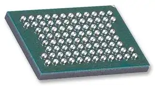
- No. of Pins: 88Pins
- Product Range: LTM4662 Series
- No. of Outputs: 2 Output
- Output Current: 15A
- Output Power Max: -
- Input Voltage Max: 20V
- Input Voltage Min: 2.375V
- Output Current Max: 15A
- Output Voltage Max: 5.5V
- Output Voltage Min: 600mV
- Switching Frequency: 1MHz
- Input Voltage DC Max: 20V
- Input Voltage DC Min: 4.5V
- DC / DC Converter Type: BGA-88, Micro Module
- DC / DC Converter IC Case: BGA
- Operating Temperature Max: 125°C
- Power Supply Applications: ITE, Industrial & Medical
- DC / DC Converter Output Type: Adjustable
| Delivery and price | |
|---|---|
| Units per pack | 112 |
| Price | 47.73 € |
| Current stock | 10+ |
| Lead time | 30 days |
LTM4662 ## Dual 15A or Single 30A DC/DC µModule Regulator ## **FEATURES** - n **Dual 15A or Single 30A Output** - n **Wide Input Voltage Range: 4.5V to 20V** - n **2.375VMIN with CPWR Bias** - n **Output Voltage Range: 0.6V to 5.5V** - n **±1.5% Maximum Total DC Output Error** - n **Multiphase Current Sharing** - n Differential Remote Sense Amplifier, Each Channel - n Current Mode Control/Fast Transient Response - n Up to 96% Efficiency - n Adjustable Switching Frequency (250kHz to 1MHz) - n Frequency Synchronization - n Overcurrent Foldback Protection - n Output Overvoltage Protection - n Internal or External Compensation - n Built-In Temperature Monitor Diode - n SnPb or RoHS Compliant Finish - n Thermally Enhanced (11.25mm × 15mm × 5.74mm) BGA Package - n Pin-Compatible with the LTM4646 ## **APPLICATIONS** - n Point-of-Load Power Supplies - n Telecom and Networking Equipment ## **DESCRIPTION** The LTM[®] 4662 is a complete dual 15A output switching mode DC/DC power supply. Included in the package are the switching controller, power FETs, inductors, and all supporting components. Operating from an input voltage range of 4.5V to 20V, the LTM4662 supports two outputs each with an output voltage range of 0.6V to 5.5V, set by external resistors. Its high efficiency design delivers up to 15A continuous current for each output. Only a few input and output capacitors are needed. The device supports frequency synchronization, multiphase operation, high efficiency light load operation and output voltage tracking for supply rail sequencing and has an onboard temperature diode per channel for device temperature monitoring. High switching frequency and a current mode architecture enable a very fast transient response to line and load changes without sacrificing stability. Fault protection features include overvoltage and overcurrent protection. The power module is offered in a small footprint and thermally enhanced 11.25mm × 15mm × 5.74mm BGA package. The LTM4662 is available with SnPb or RoHS compliant terminal finish. All registered trademarks and trademarks are the property of their respective owners. - n Industrial and Medical Equipment ## **TYPICAL APPLICATION** **==> picture [524 x 197] intentionally omitted <==** **----- Start of picture text -----**<br> VIN<br>4.5V Efficiency,<br>TO 20V 10μF 12V to 0.9V, 1.2V at 15A Each<br>×4 130k<br>VIN1 VIN2 CPWR INTVCC VRNG 95<br>RUN1 MODE_PLLIN<br>RUN2 DRVCC<br>VOUT1 4.7µF VOUT2 90<br>0.9V VOUT1 VOUT2 1.2V<br>AT 15A VOUTS1 VOUTS2 AT 15A 85<br>VFB1 LTM4662 VFB2 100µF<br>100μF×4 121k 60.4k 30.1k ×4 80<br>V OUTS1 [–] VOUTS2 [–]<br>COMP1A COMP2A<br>75<br>COMP1B COMP2B<br>0.1µF TRACK/SS1 FREQ115kSGND GND TRACK/SS24662 TA01a 0.1µF PHASMD, CLKOUT, SW1, SW2TEMP1PINS NOT USED IN THIS CIRCUIT:PGOOD1, PGOOD2, EXTV [+] , TEMP1 [–] , TEMP2CC [+] , TEMP2, [–] 70 1 2 3 4 5 6 12V12V7 ININ8 TO 0.9V EFF, 300kHz TO 1.2V EFF, 350kHz 9 10 11 12 13 14 15<br>LOAD CURRENT (A)<br>4662 TA01b<br>Rev. B<br>EFFICIENCY (%)<br>**----- End of picture text -----**<br> 1 For more information www.analog.com Document Feedback LTM4662 ## **ABSOLUTE MAXIMUM RATINGS** ## **PIN CONFIGURATION** ## **(Note 1)** CPWR, VIN1, VIN2 ....................................... –0.3V to 22V VSW1, VSW2 ................................................... –2V to 22V PGOOD1, PGOOD2, RUN1, RUN2, DRVCC, INTVCC, EXTVCC, VOUT1, VOUT2, VOUTS1, VOUTS2 ..................................................... –0.3V to 6V TRACK/SS1, TRACK/SS2 ............................. –0.3V to 5V FREQ, VRNG, PHASMD, MODE_PLLIN ......................... –0.3V to (INTVCC+0.3) VOUTS1[–] (Note 6) ....................................... –0.3V to VFB1 VOUTS2[–] , VFB1 (Note 6)..............–0.3V to (INTVCC+0.3V) COMP1A, COMP2A (Note 6) ..................... –0.3V to 2.7V COMP1B, COMP2B, VFB2 .......................... –0.3V to 2.7V DRVCC Peak Output Current .................................100mA Internal Operating Temperature Range (Note 2) E- and I-Grade ................................... –40°C to 125°C MP-Grade .......................................... –55°C to 125°C Storage Temperature Range .................. –55°C to 125°C Peak Solder Reflow Package Body Temperature .... 245°C **==> picture [212 x 362] intentionally omitted <==** **----- Start of picture text -----**<br> TOP VIEW<br>1 2 3 4 5 6 7 8<br>TEMP2 [–]<br>A<br>VIN2 TEMP2 [+]<br>B<br>VOUT2 GND<br>C<br>GND SW2<br>VRNG SGND [V] OUTS2 [–] RUN2<br>D<br>COMP2B VOUTS2 COMP2A VFB2 PGOOD2 EXTVCC<br>E<br>MODE_<br>FREQ TRACK/SS2 PLLIN CLKOUT INTVCC CPWR<br>F<br>COMP1B VOUTS1 COMP1A VFB1 PGOOD1 DRVCC<br>G<br>PHASMD SGND TRACK/SS1 RUN1<br>H<br>VOUTS1 [–] GND SW1<br>J<br>VOUT1 TEMP1 [–]<br>K<br>GND VIN1 TEMP1 [+]<br>L<br>BGA PACKAGE<br>88-LEAD (15mm × 11.25mm × 5.74mm)<br>TJMAX = 125°C, θJA = 7°C/W, θJCbottom = 1.5°C/W,<br>θJCtop = 3.7°C/W, θJB + θBA ≅ 7°C/W<br>θ VALUES DEFINED PER JESD51-12<br>WEIGHT = 2.2g<br>**----- End of picture text -----**<br> ## **ORDER INFORMATION** |**PART NUMBER**|**BALL FINISH**|**PART MARKING***|**PART MARKING***|**PACKAGE**<br>**TYPE**|**MSL**<br>**RATING**|**TEMPERATURE RANGE**<br>**(SEE NOTE 2)**| |---|---|---|---|---|---|---| |||**DEVICE**|**FINISH CODE**|||| |LTM4662EY#PBF|SAC305 (RoHS)|LTM4662Y|e1|BGA|3|–40°C to 125°C| |LTM4662IY#PBF||LTM4662Y||||–40°C to 125°C| |LTM4662MPY#PBF||LTM4662Y||||–55°C to 125°C| |LTM4662IY|SnPb (63/37)|LTM4662Y|e0|||–40°C to 125°C| |LTM4662MPY||LTM4662Y||||–55°C to 125°C| - Contact the factory for parts specified with wider operating temperature ranges. *Device temperature grade is indicated by a label on the shipping container. Ball finish code is per IPC/JEDEC J-STD-609. - Recommended LGA and BGA PCB Assembly and Manufacturing Procedures - LGA and BGA Package and Tray Drawings Rev. B 2 For more information www.analog.com LTM4662 ## **ELECTRICAL CHARACTERISTICS** **The** l **denotes the specifications which apply over the specified internal operating temperature range (Note 2). Specified as each individual output channel. TA = 25°C, VIN = 12V and VRUN1, VRUN2 at 5V unless otherwise noted. Per the typical application in Figure 20.** |**SYMBOL**||**PARAMETER**|**CONDITIONS**||**MIN**|**TYP**|**MAX**|**UNITS**| |---|---|---|---|---|---|---|---|---| |VIN(DC)||Input DC Voltage|2.375V with 5V External Bias on CPWR, 4.5V<br>Min without Bias|l|2.375||20|V| |VCPWR(DC)||Input Control Power Voltage|Input Range of Bias<br>NormallyConnected to VIN||4.5||20|V| |VOUT1,2(Range)||Output Voltage Range|(Note 8)|l|0.6||5.5|V| |VOUT1(DC),<br>VOUT2(DC)||Output Voltage, Total Variation<br>with Line and Load|CIN= 10µF×4, COUT= 100µF×4 Ceramic<br>VOUT= 1.5V|l|1.4775|1.5|1.5225|V| |**Input Specifications**||||||||| |VRUN1, VRUN2||RUN Pin On/Off Threshold|RUN Rising||1.1|1.2|1.3|V| |VRUN1HYS, VRUN2HYS||RUN Pin On Hysteresis||||160||mV| |RRUN1, RRUN2||RUN1, RUN2 Resistance|Pull-Down Resistance|||100||kΩ| |IINRUSH(VIN)||Input Inrush Current at Start-Up|IOUT= 0A, CIN= 10µF ×4, CSS= 0.01µF,<br>COUT= 100µF ×4, VOUT1= 1.5V, VOUT2= 1.5V,|||1||A| ||||VIN= 12V|||||| |IQ(VIN)||Input Supply Bias Current|IOUT= 0.1A, fSW= 1MHz, Pulse-Skipping Mode<br>IOUT= 0.1A, fSW= 1MHz, Switching Continuous|||20<br>45||mA<br>mA| ||||Shutdown, RUN = 0, VIN= 12V|||40||µA| |IS(VIN)||Input Supply Current|VIN= 4.5V, VOUT= 1.5V, IOUT= 15A<br>VIN= 12V, VOUT= 1.5V, IOUT= 15A|||5.9<br>2.15||A<br>A| |**Output Specifications**||||||||| |IOUT1(DC), IOUT2(DC)||Output Continuous Current Range|VIN= 12V, VOUT= 1.5V(Notes 7, 8)||0||15|A| |ΔVOUT1(LINE)/VOUT1<br>ΔVOUT2(LINE)/VOUT2||Line Regulation Accuracy|VOUT= 1.5V, VINfrom 4.5V to 20V<br>IOUT= 0A for Each Output|l||0.01|0.025|%/V| |ΔVOUT1(LOAD)/VOUT1<br>ΔVOUT2(LOAD)/VOUT2||Load Regulation Accuracy|For Each Output, VOUT= 1.5V, 0A to 15A<br>VIN= 12V(Note 7)|l||0.15|0.3|%| |VOUT1(AC), VOUT2(AC)||Output Ripple Voltage|For Each Output, IOUT= 0A,<br>COUT= 100µF ×4, VIN= 12V,|||15||mVP-P| ||||VOUT= 1.5V, Frequency= 350kHz|||||| |fS (Each Channel)||Output Ripple Voltage Frequency|VIN= 12V, VOUT= 1.5V, RFREQ= 115kΩ(Note 4)|||350||kHz| |ΔVOUTSTART||Turn-On Overshoot|COUT= 100µF ×4, VOUT= 1.5V, IOUT= 0A|||10||mV| |(Each Channel)|||VIN= 12V, CSS= 0.01µF|||||| |tSTART||Turn-On Time|COUT= 100µF ×4, No Load,|||5||ms| |(Each Channel)|||TRACK/SS with 0.01µF to GND, VIN= 12V|||||| |ΔVOUT(LS)<br>(Each Channel)||Peak Deviation for Dynamic Load|Load: 0A to 6A to 0A<br>COUT= 100µF ×4,|||50||mV| ||||VIN= 12V, VOUT= 1.5V|||||| |tSETTLE||Settling Time for Dynamic Load Step|Load: 0A to 6A to 0A|||20||µs| |(Each Channel)|||COUT= 100µF ×4,|||||| ||||VIN= 12V, VOUT= 1.5V|||||| |IOUT(PK)<br>(Each Channel)||Output Current Limit|VIN= 12V, VOUT= 1.5V|||22||A| Rev. B 3 For more information www.analog.com ## LTM4662 ## **ELECTRICAL CHARACTERISTICS** **The** l **denotes the specifications which apply over the specified internal operating temperature range (Note 2). Specified as each individual output channel. TA = 25°C, VIN = 12V and VRUN1, VRUN2 at 5V unless otherwise noted. Per the typical application in Figure 20.** |**SYMBOL**|**PARAMETER**|**CONDITIONS**|**CONDITIONS**|**MIN**<br>**TYP**<br>**MAX**|**UNITS**| |---|---|---|---|---|---| |**Control Section**|||||| |VFB1|Voltage at VFB1Pin|IOUT= 0A, VOUT= 1.5V|l|0.592<br>0.600<br>0.608|V| |VFB2|Voltage at VFB2Pin|IOUT= 0A, VOUT= 1.5V<br>VFB2is Gained Back Upby2× Internal to 0.6V|l|0.296<br>0.3<br>0.304|V| |IFB1, IFB2||(Note 6)||0<br>±50|nA| |VOVL1,VOVL2|Feedback Overvoltage Lockout|VFB1Rising, VFB2Rising|l|0.630<br>0.315<br>0.645<br>0.323<br>0.660<br>0.330|V<br>V| |ITRACK/SS1,<br>ITRACK/SS2|Track Pin Soft-Start Pull-Up Current|TRACK/SS1,TRACK/SS2 = 0V||1.0|µA| |UVLO|INTVCCUndervoltage Lockout|INTVCCFalling VIN(Note 6)<br>INTVCCRisingVIN||3.3<br>3.7<br>4.2<br>4.5|V<br>V| |tOFF(MIN)|Minimum TopGate Off-Time|(Note 6)||90|ns| |tON(MIN)|Minimum TopGate On-Time|(Note 6)||30|ns| |RFBHI1, RFBHI2|Resistor Between VOUTS1, VOUTS2<br>and VFB1, VFB2Pins for Each Output|||59.9<br>60.4<br>60.9|kΩ| |VPGOOD1, VPGOOD2<br>Low|PGOOD Voltage Low|IPGOOD= 2mA||0.1<br>0.3|V| |IPGOOD|PGOOD Leakage Current|VPGOOD= 5V||–2<br>2|µA| |VPGOOD|PGOOD Trip Level|VFBwith Respect to Set Output Voltage<br>VFBRamping Negative<br>VFBRampingPositive||–7.5<br>7.5|%<br>%| |**Internal Linear Regulator**|||||| |DRVCC|Internal DRVCCVoltage|6V < CPWR < 20V||5.0<br>5.3<br>5.6|V| |DRVCC<br>Load Regulation|DRVCCLoad Regulation|ICC= 0mA to 100mA||–1.3<br>–3.0|%| |VEXTVCC|EXTVCCSwitchover Voltage|EXTVCCRampingPositive||4.4<br>4.6<br>4.8|V| |VEXTVCC(DROP)|EXTVCCDropout|ICC= 20mA, VEXTVCC= 5V||80<br>120|mV| |VEXTVCC(HYST)|EXTVCCHysteresis|||200|mV| |**Frequency and Clock Synchronization**|||||| |FrequencyNominal|Nominal Frequency|RFREQ= 115kΩ||300<br>350<br>400|kHz| |FrequencyLow|Lowest Frequency|RFREQ= 165kΩ(Note 5)||250|kHz| |FrequencyHigh|Highest Frequency|RFREQ= 39.2kΩ||900<br>1000<br>1100|kHz| |RMODE_PLLIN|MODE_PLLIN Input Resistance|MODE_PLLIN to SGND||600|kΩ| |Channel 2 Phase|VOUT2Phase Relative to VOUT1|PHASMD = SGND<br>PHASMD = Float<br>PHASMD = INTVCC||180<br>180<br>240|Deg<br>Deg<br>Deg| |CLKOUT Phase|Phase (Relative to VOUT1)|PHASMD = SGND<br>PHASMD = Float<br>PHASMD = INTVCC||60<br>90<br>120|Deg<br>Deg<br>Deg| |VPLLINHigh<br>VPLLINLow|Clock Input High Level to MODE_PLLIN<br>Clock Input Low Level to MODE_PLLIN|||2<br>0.5|V<br>V| Rev. B 4 For more information www.analog.com LTM4662 **ELECTRICAL CHARACTERISTICS The** l **denotes the specifications which apply over the specified internal operating temperature range (Note 2). Specified as each individual output channel. TA = 25°C, VIN = 12V and VRUN1, VRUN2 at 5V unless otherwise noted. Per the typical application in Figure 20.** |**SYMBOL**|**PARAMETER**|**CONDITIONS**|**CONDITIONS**|**MIN**<br>**TYP**<br>**MAX**|**UNITS**<br>kHz<br>A<br>A<br>μs<br>μs<br>V<br>mV/°C| |---|---|---|---|---|---| |fSYNC<br>(Each Channel)|Frequency Sync Capture Range|MODE_PLLIN Clock Duty Cycle = 50%||250<br>1000|| |VRNG ILIMIT|SET Current Limit<br>Per Channel|VRNG = INTVCC, IOUTto 15A, ILIMIT~22A<br>VRNG = SGND, IOUTto 7.5A, ILIMIT~11A||15<br>7.5|| |tD(PGOOD)|Delay from VFBFault (OV/UV) to<br>PGOOD Falling|(Note 6)||50|| |tD(PGOOD)|Delay from VFBFault (OV/UV Clear)<br>to PGOOD|(Note 6)||20|| |VTEMP1, VTEMP2|TEMP Diode Voltage|ITEMP= 100µA||0.598|| |TCVTEMP1,2|VTEMPTemperature Coefficient|||–2.0|| **Note 1:** Stresses beyond those listed under Absolute Maximum Ratings may cause permanent damage to the device. Exposure to any Absolute Maximum Rating condition for extended periods may affect device reliability and lifetime. **Note 2:** The LTM4662 is tested under pulsed load conditions such that TJ ≈ TA. The LTM4662E is guaranteed to meet specifications from 0°C to 125°C internal temperature. Specifications over the –40°C to 125°C internal operating temperature range are assured by design, characterization and correlation with statistical process controls. The LTM4662I is guaranteed over the full –40°C to 125°C internal operating temperature range. The LTM4662MP is tested and guaranteed over full –55°C to 125°C internal operating temperature range. Note that the maximum ambient temperature consistent with these specifications is determined by specific operating conditions in conjunction with board layout, the rated package thermal impedance and other environmental factors. **Note 3:** Two outputs are tested separately and the same testing condition is applied to each output. **Note 4:** The switching frequency is programmable from 250kHz to 1000kHz. **Note 5:** LTM4662 device is optimized to operate from 300kHz to 750kHz. **Note 6:** These parameters are tested at wafer sort. **Note 7:** See output current derating curves for different VIN, VOUT and TA. **Note 8:** For 6V ≤ VIN ≤ 20V, the 3.3 to 5V output current needs to be limited to 13A/channel. All other input and output combinations are 15A/ channel with recommended switching frequency included in the efficiency graphs. Derating curves and airflow apply. Rev. B 5 For more information www.analog.com ## LTM4662 ## **TYPICAL PERFORMANCE CHARACTERISTICS** **==> picture [526 x 622] intentionally omitted <==** **----- Start of picture text -----**<br> Efficiency vs Output Current, Efficiency vs Output Current, Efficiency vs Output Current,<br>VIN = 5V VIN = 8V VIN = 12V<br>100 100 100<br>95 95 95<br>90 UT TTT 90 ; se. 90 Ph EE]<br>Be) SSE) pee<br>85 POSS 85 ff 8V IN TO 0.9V EFF, 350kHz SSS 85 12V IN TO 0.9V EFF, 300kHz See<br>5VIN TO 0.9V EFF, 350kHz 8VIN TO 1.0V EFF, 350kHz 12VIN TO 1.0V EFF, 300kHz<br>80 5VIN TO 1.0V EFF, 350kHz l e e 80 8V IN TO 1.2V EFF, 350kHz ee 80 12V IN TO 1.2V EFF, 350kHz |<br>5VIN TO 1.2V EFF, 350kHz 8VIN TO 1.5V EFF, 450kHz 12VIN TO 1.5V EFF, 450kHz<br>5VIN TO 1.5V EFF, 350kHz 8VIN TO 1.8V EFF, 500kHz 12VIN TO 1.8V EFF, 500kHz<br>75 - 5V IN TO 1.8V EFF, 450kHz i l e 75 8VIN TO 2.5V EFF, 600kHz | 75 4 12VIN TO 2.5V EFF, 650kHz |<br>5VIN TO 2.5V EFF, 450kHz 8VIN TO 3.3V EFF, 750kHz 12VIN TO 3.3V EFF, 800kHz<br>5VIN TO 3.3V EFF, 450kHz 8VIN TO 5.0V EFF, 950kHz 12VIN TO 5.0V EFF, 950kHz<br>70 - i ee e 70 | 70 oo |<br>1 2 3 4 5 6 7 8 9 10 11 12 13 14 15 1 2 3 4 5 6 7 8 9 10 11 12 13 14 15 1 2 3 4 5 6 7 8 9 10 11 12 13 14 15<br>LOAD CURRENT (A) LOAD CURRENT (A) LOAD CURRENT (A)<br>4662 G01 4662 G02 4662 G03<br>Dual Phase Single Output Efficiency 0.9V Single Phase Single Output 1V Single Phase Single Output<br>vs Output Current, VIN = 12V Load Transient Response Load Transient Response<br>100<br>EXTVCC = 5V<br>95<br>pee) =| AR--J p<br>IOUT IOUT<br>90 (eee| 7.5A/DIV =| 7.5A/DIV | 7<br>85<br>80 /|ALLL 12V–1V EFF, 300kHz 12V LLL –1.2V EFF, 300kHz LTTSSS) 50mV/DIV0.9VOUT ToeLos 50mV/DIV1VOUT Fe- R<br>12V–1.5V EFF, 350kHz<br>12V–1.8V EFF, 450kHz pore preety on? ne<br>75 12V–2.5V EFF, 650kHz 50µs/DIV 4662 G05 50µs/DIV 4662 G06<br>12V–3.3V EFF, 800kHz<br>12V–5V EFF, 950kHz COUT = 470µF POSCAP, 5mΩ, COUT = 470µF POSCAP, 5mΩ,<br>70 - il 100µF ×4, CERAMIC 100µF ×4, CERAMIC<br>1 4 6 8 10 12 14 16 18 20 22 24 26 28 30 CCOMP = 100pF, CCOMP = 100pF,<br>LOAD CURRENT (A) f = 350kHz f = 350kHz<br>4662 G04<br>1.2V Single Phase Single Output 1.5V Single Phase Single Output 1.8V Single Phase Single Output<br>Load Transient Response Load Transient Response Load Transient Response<br>IEEE<br>IOUT IOUT IOUT<br>7.5A/DIV 7.5A/DIV 7.5A/DIV<br>eo) fea fe<br>REE BRS Se<br>1.2VOUT 1.5VOUT 1.8VOUT<br>50mV/DIV —— 50mV/DIV -—— 50mV/DIV 4+—t<br>Oe ee Pee Se<br>50µs/DIV 4662 G07 50µs/DIV 4662 G08 50µs/DIV 4662 G09<br>COUT = 470µF POSCAP, 5mΩ, COUT = 100µF ×3, CERAMIC COUT = 100µF ×3, CERAMIC<br>100µF ×4, CERAMIC CCOMP = 100pF, CFF = 47pF CCOMP = 100pF, CFF = 47pF<br>CCOMP = 100pF, f = 450kHz f = 500kHz<br>f = 350kHz<br>Rev. B<br>EFFICIENCY (%) EFFICIENCY (%) EFFICIENCY (%)<br>EFFICIENCY (%)<br>**----- End of picture text -----**<br> 6 For more information www.analog.com LTM4662 ## **TYPICAL PERFORMANCE CHARACTERISTICS** **2.5V Single Phase Single Output Load Transient Response** **3.3V Single Phase Single Output Load Transient Response** **==> picture [347 x 363] intentionally omitted <==** **----- Start of picture text -----**<br> 7.5A/DIVIOUT FE) IOUT EE<br>5A/DIV<br>2.5VOUT 3.3VOUT<br>100mV/DIV 100mV/DIV<br>foiSeS e e aeEODEE.<br>50µs/DIV 4662 G10 50µs/DIV 4662 G11<br>COUT = 100µF ×2, CERAMIC COUT = 100µF ×1, CERAMIC<br>CCOMP = 100pF, CFF = 47pF CCOMP = 100pF, CFF = 47pF<br>f = 500kHz f = 750kHz<br>Single Phase Single Output Single Phase Single Output<br>Start-Up, No Load Start-Up, 15A Load<br>VOUT VOUT<br>0.5V/DIV 0.5V/DIV<br>IOUT IOUT<br>1A/DIV 10A/DIV<br>|) (ees<br>50ms/DIV 4662 G13 20ms/DIV 4662 G14<br>12VIN, 1.5VOUT AT NO LOAD 12VIN, 1.5VOUT AT 15A LOAD<br>COUT = 470µF ×1, 2.5V, SANYO POSCAP, COUT = 470µF ×1, 2.5V, SANYO POSCAP,<br>100µF ×4, 6.3V, CERAMIC 100µF ×4, 6.3V, CERAMIC<br>SOFT-START CAPACITOR = 0.1µF SOFT-START CAPACITOR = 0.1µF<br>USE RUN PIN TO CONTROL START-UP USE RUN PIN TO CONTROL START-UP<br>**----- End of picture text -----**<br> **5V Single Phase Single Output Load Transient Response** **==> picture [169 x 107] intentionally omitted <==** **----- Start of picture text -----**<br> IOUT<br>5A/DIV<br>5VOUT<br>100mV/DIV<br>50µs/DIV 4662 G12<br>COUT = 100µF ×1, CERAMIC<br>CCOMP = 100pF, CFF = 47pF<br>f = 950kHz<br>**----- End of picture text -----**<br> ## **Two-Phase Switching and Ripple** **==> picture [162 x 118] intentionally omitted <==** **----- Start of picture text -----**<br> VOUT<br>5V/DIV<br>VOUT<br>10mV/DIV<br>op<br>1µs/DIV 4662 G15<br>12V TO 1V AT 30A TWO-PHASE<br>12V TO 1V AT 350kHz<br>RIPPLE AT 30A LOAD<br>COUT = 330μF, 9mΩ, 100μF ×4, CERAMIC<br>**----- End of picture text -----**<br> **Short-Circuit Protection, No Load** **Short-Circuit Protection, 15A Load** **==> picture [384 x 118] intentionally omitted <==** **----- Start of picture text -----**<br> VOUT VOUT<br>500mV/DIV 500mV/DIV<br>Pe i<br>IIN<br>IOUT 1A/DIV<br>1A/DIV<br>——<br>20ms/DIV 4662 G16 20ms/DIV 4662 G17<br>VVIOUTINOUT = 12V = NO LOAD= 1.5V VVIOUTINOUT = 12V = 15A= 1.5V<br>**----- End of picture text -----**<br> Rev. B 7 For more information www.analog.com LTM4662 ## **PIN FUNCTIONS** ## **(Recommended to Use Test Points to Monitor Signal Pin Connections.)** An external clock applied to MODE_PLLIN should be within ±30% of this programmed frequency to ensure frequency lock. See the Applications Information section. ## **PACKAGE ROW AND COLUMN LABELING MAY VARY AMONG µModule PRODUCTS. REVIEW EACH PACKAGE LAYOUT CAREFULLY.** **==> picture [35 x 31] intentionally omitted <==** **VOUT1 (H1, J1-J2, K1-K2, L1-L2):** Power Output Pins. Apply output load between these pins and GND pins. Recommend placing output decoupling capacitance directly between these pins and GND pins. There is a 49.9Ω resistor connected between VOUT1 and VOUTS1 to protect the output from an open VOUTS1. Review Table 5. See Note 8 in the Electrical Characteristics section for output current guideline. **SGND (D3, H3):** Signal Ground Pin. Return ground path for all analog and low power circuitry. Tie a single connection to the output capacitor GND in the application. See layout guidelines in Figure 19. **VFB1 (G4):** This pin is the + input to a unity gain differential amplifier. This pin is connected to VOUTS1 with a 60.4k precision resistor internal. Different output voltages can be programmed with an additional resistor between VFB1 and VOUTS1[– ] pins. The differential amplifier is feeding back the divided down output voltage from a remote sense divider network to compare to the internal 0.6V reference. In 2-phase single output operation, tie the VFB1 pin to INTVCC. See Figure 1 and Applications Information section for details. **GND (A3, A6-A7, B3, B6-B7, C3-C7, D6-D7, E6, E8, F5, F7, G6, G8, H6-H7, J4-J7, K3, K6-K7, L3, L6-L7 ):** Power Ground Pins for Both Input and Output Returns. **VOUT2 (A1-A2, B1-B2, C1-C2, D1):** Power Output Pins. Apply output load between these pins and GND pins. Recommend placing output decoupling capacitance directly between these pins and GND pins. There is a 49.9Ω resistor connected between VOUT2 and VOUTS2 to protect the output from an open VOUTS2. Review Table 5. See Note 8 in the Electrical Characteristics section for output current guideline. **VFB2 (E4):** This pin is the + input to a non-inverting gain of two amplifier utilizing three resistors in the feedback network to develop a remote sense divider network. This pin is connected to VOUTS2 with an internal 60.4k precision resistor. The VOUT2 voltage is divided down to 0.3V then gained back up to 0.6V to compare with the internal 0.6V reference. This technique provides for equivalent remote sensing on VOUT2. See Figure 1 and Applications Information section for details. **VOUTS1, VOUTS2 (G2, E2):** These pins are connected to the top of the internal top feedback resistor for each output. Each pin can be directly connected to its specific output, or connected to the remote sense point of VOUT. It is important to connect these pins to their designated outputs for proper regulation. **TRACK/SS1,TRACK/SS2 (H4, F2):** Output Voltage Tracking Pin and Soft-Start Inputs. Each channel has a 1.0μA pull-up current source. Each pin can be programmed with a softstart ramp rate up to the 0.6V internal reference level, then beyond this point the internal 0.6V reference will control the feedback loop. When one channel is configured to be master of the two channels, then a capacitor from this pin to ground will set the soft-start ramp rate. The remaining channel can be set up as the slave, and have the master’s output applied through a voltage divider to the slave output’s track pin. This voltage divider is equal to the slave output’s feedback divider for coincidental tracking. See the Applications Information section. (Recommended to use test points to monitor signal pin connections.) In paralleling modules, the VOUTS1 pin is left floating, and the VFB1 pin is connected to INTVCC. This will disable channel 1’s error amplifier and internally connect COMP1A to COMP2A. The PGOOD1 and TRACK/SS1 will be disabled in this mode. Channel 2’s error amplifier will regulate the two channel single output. See VFB pin description and Applications Information section. **FREQ (F1):** Frequency Set Pin. A resistor from this pin to SGND sets the operating frequency. The Equation: 41550 – 2.2 = RFREQ(kΩ) f(kHz) **DRVCC (G7):** Internal 5.3V regulator output used to source the power MOSFET drivers, and supply power to the INTVCC input. A 4.7µF ceramic capacitor is needed on this pin to GND. Rev. B 8 For more information www.analog.com LTM4662 ## **PIN FUNCTIONS (Recommended to Use Test Points to Monitor Signal Pin Connections.)** **CPWR (F8):** Input Power to the Control IC, and Power to the DRVCC Regulator. This pin is connected to VIN for normal 4.5V to 20V operation. For lower voltage inputs below 4.5V, CPWR can be powered with an external 5V bias. See Application section. **COMP1A, COMP2A (G3, E3):** Current Control Threshold. These pins are the output of the error amplifier and the switching regulator’s compensation point. The current comparator threshold increases with this control voltage. The voltage ranges from 0V to 2.4V. **COMP1B, COMP2B (G1, E1):** Internal Compensation Network .These pins are to be connected to their respected COMPA pins. When Utilizing specific external compensation, then float these pins. **MODE_PLLIN (F3):** Operation Mode Selection or External Clock Synchronization Input. When this pin is tied to INTVCC, forced continuous mode operation is selected. Tying this pin to SGND allows discontinuous mode operation. When an external clock is applied at this pin, both channels operate in forced continuous mode and synchronize to the external clock. This pin has an internal 600k pull-down resistor to SGND. An external clock applied to MODE_PLLIN should be within ±30% of this programmed frequency to ensure frequency lock. **CLKOUT (F4):** Clock output with phase control using the PHASMD pin to enable multiphase operation between devices. Its output level swings between INTVCC and SGND. If clock input is present at the MODE_PLLIN pin, it will be synchronized to the input clock, with phase set by the PHASMD pin. If no clock is present at MODE_PLLIN, its frequency will be set by the FREQ pin. To synchronize other controllers, it can be connected to their MODE_PLLIN pins. See the Applications Information section. **RUN1, RUN2 (H5, D5):** Run Control Pins. A voltage above 1.3V will turn on each channel in the module. A voltage below 1.0V on the RUN pin will turn off the related channel. Each RUN pin has a 1.2μA pull-up current, once the RUN pin reaches 1.2V an additional 4.5μA pull-up current is added to this pin. A 100k resistor to ground is internal, and can be used with a pull-up resistor to VIN to turn on the module using the external and internal resistor to program under voltage lockout. Otherwise, an external enable signal or source can drive these pins directly below the 6V max. Enabling either RUN pin will turn on the DRVCC, and turn on the INTVCC path for operation. See Figure 1 and Applications section. **PHASMD (H2):** Connect this pin to SGND, INTVCC, or floating this pin to select the phase of CLKOUT and channel 2. See Electrical Characteristics table and Application section. **PGOOD1, PGOOD2 (G5, E5):** Output Voltage Power Good Indicator. Open-drain logic output that is pulled to ground when the output voltage is not within ±7.5% of the regulation point. See Applications section. **INTVCC (F6):** Supply Input for Internal Circuitry (Not Including Gate Drivers). This bias is derived from DRVCC internally. **EXTVCC (E7):** External Power Input. When EXTVCC exceeds the switchover voltage (typically 4.6V), an internal switch connects this pin to DRVCC and shuts down the internal regulator so that INTVCC and gate drivers draw power from EXTVCC. The VIN pin still needs to be powered up but draws minimum current. **TEMP1[+] ,TEMP1[–] and TEMP2[+] , TEMP2[–] (L8, K8 and B8, A8):** Onboard temperature diode for monitoring each channel with differential connections for noise immunity. **VIN1 (K4-K5, L4-L5) and VIN2 (A4-A5, B4-B5):** Power Input Pins. Apply input voltage between these pins and GND pins. Recommend placing input decoupling capacitance directly between VIN pins and GND pins. **VOUTS1[–] (J3):** Differential Output Sense Amplifier (–) Input of channel 1. Connect this pin to the negative terminal of the output load capacitor of VOUT1. **VOUTS2[–] (D4):** Differential Output Sense Amplifier (–) Input of channel 2. Connect this pin to the negative terminal of the output load capacitor of VOUT2. **SW1 (H8, J8) and SW2 (C8, D8):** Switching node of each channel that is used for testing purposes. Also an R-C snubber network can be applied to reduce or eliminate switch node ringing, or otherwise leave floating. See the Applications Information section. **VRNG (D2):** Current Limit Adjustment Range. Tying this pin to INTVCC sets full 15A current, or tying to SGND will lower the current limit to 7.5A. Default to INTVCC. Rev. B 9 For more information www.analog.com LTM4662 ## **BLOCK DIAGRAM** **==> picture [520 x 626] intentionally omitted <==** **----- Start of picture text -----**<br> CPWR CPWR<br>EXTVCC DRVCC<br>LDO<br>DRVCC VIN VIN VIN 4.5V TO 20V<br>4.7µF 2Ω 1µF DRVCC 1µF GND C10µF25VIN1 C10µF25VIN2 + 100µF25V<br>INTVCC TOP G MTOP1<br>1µF SW1<br>COMP1A GATE 0.47µH VOUT1 1.5V/15A<br>DRIVE<br>COMP1B +<br>RUN1 AND RUN2 BOT G MBOT1 1µF COUT1<br>TIED TOGETHER:RPULLUP = VIN INTERNALCOMP GND<br>VIN(MIN) • 50k – 50k 130k SGND – VFB1<br>( 1.3 ) RUN1 gm + VOUTS1 [–]<br>RUN1 AND RUN2 100k + +– 0.6VREF ×1 RFB1<br>SEPARATE:RPULLUP = RUN2 SGND VOUT1 VFB1 40.2k<br>VIN(MIN) • 100k – 100k 100k SS 60.4k<br>( 1.3 ) CLKOUT POWER 49.9Ω VOUTS1<br>CONTROL<br>INTVCC MODE_PLLIN BLOCKLOGIC 1µA LOCATED NEAR POWER STAGES TEMP1 [+]<br>PHASMD TEMP SENSOR<br>RFREQ = ( [41550] f(kHz) ) – 2.2 FREQ 0.645V – NPN 470pF TEMP1 [–]<br>115k VFB1 + PGOOD1 PGOOD1<br>350kHz INTVC C VRNG – BLOCK<br>SGND 0.555V +<br>VIN VIN<br>tSOFT-START = ( 1µA [C][SS] ) • 0.6V TRACK/SS1 DRVCC C81µF C10µF25VIN3 C10µF25VIN4<br>GND<br>MTOP2 SW2<br>CSS<br>SGND COMP2A GATE 0.47µH VOUT2 VOUT2 1.2V/15A<br>DRIVE<br>+<br>COMP2B MBOT2 1µF COUT2<br>GND<br>INTERNAL<br>COMP R7<br>50k 50k VOUTS2 [–]<br>SGND<br>SS – VFB2 0.6V ×2 R60.4kFB2 RFB3<br>gm + 0.3V VFB2 30.1k<br>1µA + +– 0.6V REF VOUT2<br>TRACK/SS2 60.4k SGND<br>SGND<br>49.9Ω<br>VOUTS2<br>CSS PGOOD2 – 0.645V POWER STAGESLOCATED NEAR<br>TEMP2 [+]<br>SGND PGOOD2 VFB1<br>BLOCK +<br>– NPN 470pF TEMP SENSOR<br>TEMP2 [–]<br>+ 0.555V<br>4662 F01<br>Figure 1. Simplified LTM4662 Block Diagram<br>Rev. B<br>–<br>+<br>–<br>+<br>**----- End of picture text -----**<br> 10 For more information www.analog.com LTM4662 ## **DECOUPLING REQUIREMENTS TA = 25°C. Use Figure 1 configuration.** |**DECO**|**UPLING REQUIREMENTS**|**TA = 25°C. Use Figure 1 configuration.**|**TA = 25°C. Use Figure 1 configuration.**||| |---|---|---|---|---|---| |**SYMBOL**|**PARAMETER**|**CONDITIONS**||**MIN**<br>**TYP**<br>**MAX**|**UNITS**| |CIN1,CIN2<br>CIN3, CIN4|External Input Capacitor Requirement<br>(VIN= 4.5V to 20V, VOUT1= 1.5V)<br>(VIN= 4.5V to 20V, VOUT2= 1.5V)|IOUT1= 15A<br>10μF ×2<br>IOUT2= 15A<br>10μF ×2(Note 8)||20<br>20|µF<br>µF| |COUT1<br>COUT2|External Output Capacitor Requirement<br>(VIN= 4.5V to 20V, VOUT1= 1.5V)<br>(VIN= 4.5V to 20V, VOUT2= 1.5V)|IOUT1= 15A<br>IOUT2= 15A(Note 8)||400<br>400|µF<br>µF| ## **OPERATION** ## **Power Module Description** The LTM4662 is a dual-output standalone non-isolated switching mode DC/DC power supply. It can provide two 15A outputs with few external input and output capacitors and setup components. This module provides precisely regulated output voltages programmable via external resistors from 0.6VDC to 5.5VDC over 4.5V to 20V input voltages. The typical application schematic is shown in Figure 20. See Note 8 in the Electrical Characteristics section for output current guideline. The LTM4662 has dual integrated controlled-on time current mode regulators and built-in power MOSFET devices with fast switching speed. The controlled on-time, valley current mode control architecture, allows for not only fast response to transients without clock delay, but also constant frequency switching at steady load condition. The typical switching frequency is 400kHz. For switchingnoise sensitive applications, it can be externally synchronized from 250kHz to 1000kHz. A resistor can be used to program a free run frequency on the FREQ pin. See the Applications Information section. With current mode control and internal feedback loop compensation, the LTM4662 module has sufficient stability margins and good transient performance with a wide range of output capacitors, even with all ceramic output capacitors. Optimized external compensation is supported by disconnecting the internal compensation. Current mode control provides cycle-by-cycle fast current limit and foldback current limit in an overcurrent condition. Internal overvoltage and undervoltage comparators pull the open-drain PGOOD outputs low if the output feedback voltage exits a ±7.5% window around the regulation point. As the output voltage exceeds 7.5% above regulation, the bottom MOSFET will turn on to clamp the output voltage. The top MOSFET will be turned off. This overvoltage protect is feedback voltage referred. Pulling the RUN pins below 1.3V forces the regulators into a shutdown state, by turning off both MOSFETs. The TRACK/SS pins are used for programming the output voltage ramp and voltage tracking during start-up or used for soft-starting the regulator. See the Applications Information section. The LTM4662 is internally compensated to be stable over all operating conditions. Table 5 provides a guideline for input and output capacitances for several operating conditions. The LTpowerCAD[®] will be provided for transient and stability analysis. The VFB1 pin is used to program the channel 1 output voltage with a single external resistor to ground, and VFB2 pin requires two resistors to program the output. Both channel 1 and 2 have remote sense capability. Multiphase operation can be easily employed with the MODE_PLLIN, PHASMD, and CLKOUT pins. Up to 6 phases can be cascaded to run simultaneously with respect to each other by programming the PHASMD pin to different levels. See the Applications Information section. High efficiency at light loads can be accomplished with selectable pulse-skipping operation using the MODE_PLLIN. These light load features will accommodate battery operation. Efficiency graphs are provided for light load operation in the Typical Performance Characteristics section. Each channel has temperature diode included inside the module to monitor the temperature of the module. See the Applications Information section for details. Rev. B 11 For more information www.analog.com LTM4662 ## **APPLICATIONS INFORMATION** The typical LTM4662 application circuit is shown in Figure 20. External component selection is primarily determined by the maximum load current and output voltage. Refer to Table 5 for specific external capacitor requirements for particular applications. ## **VIN to VOUT Step-Down Ratios** There are restrictions in the maximum VIN and VOUT stepdown ratio that can be achieved for a given input voltage. Each output of the LTM4662 is capable of a wide duty cycle that is limited by the minimum on-time tON(MIN) of 30ns defined as tON(MIN) < D/fSW for narrow duty cycle, where D is duty cycle (VOUT/VIN) and fSW is the switching frequency. The minimum off-time of 90ns tOFF(MIN) < 1 – D/fSW is required for higher duty cycles. See Note 8 in the Electrical Characteristics section for output current guideline. ## **Output Voltage Programming** The PWM controller has an internal 0.6V reference voltage. As shown in Figure 1, a 60.4k internal feedback resistor connects between the VOUTS1 to VFB1 and VOUTS2 to VFB2. It is very important that these pins be connected to their respective outputs for proper feedback regulation. Each channel has a 49.9Ω resistor connected from VOUTS1 and VOUTS2 to VOUT1 and VOUT2, respectively. This is used to protect the output if VOUTSn is open or left unconnected. The VOUT1 output voltage will default to 0.6V with no feedback resistor on VFB1. Adding a resistor RFB1 from VFB1 pin to VOUTS1[–] programs the output voltage: **==> picture [119 x 28] intentionally omitted <==** The Thevenin equivalent of the VOUT2 equation would be the 0.6V with a series resistance of (60.4k || RFB2), thus RFB3 connected to the series resistance would be (60.4k || RFB2) to equal the 0.3V reference. **Table 1. VFB1, VFB2, Resistor Table vs Various Output Voltages** |**VOUT1**|0.6V|1.0V|1.2V|1.5V|1.8V|2.5V|3.3V|5.0V| |---|---|---|---|---|---|---|---|---| |**RFB1**|Open|90.9k|60.4k|40.2k|30.1k|19.1k|13.3k|8.25k| |**VOUT2**|0.3V|1.0V|1.2V|1.5V|1.8V|2.5V|3.3V|5.0V| |**RFB2**|Open|90.9k|60.4k|40.2k|30.1k|19.1k|13.3k|8.25k| |**RFB3**|Open|36.5k|30.1k|24.3k|20k|14.7k|11k|7.32k| Figure 2 shows the LTM4662 used in a 2-phase single output: Tie the VFB1 pin to INTVCC, which will disable channel 1’s error amplifier and internally connect COMP2 to COMP1. Tie any of the compensation components to the COMP2 pin. The COMP1 pin can be either left open or shorted to COMP2 externally as shown. The, VOUTS1, TRACK/SS1 and PGOOD1 pins become non-operable and can be left open. To make a single-output converter of three or more phases, additional LTM4662 micro modules can be used. The first module should be tied the same way as the Figure 2. If only one more channel of an additional LTM4662 is needed, use channel 2 for the additional phase: - Tie the COMP2 pin to the COMP2 pin of the first module. - Tie the RUN2 pin to the RUN pins of the first module. Use 1/2 the value for RFB2 and RFB3. - Tie VOUTS2 of the additional channel to VOUTS2 of the first module then to remote sense point. - Tie the VFB2 pin to the VFB2 pin of the first module. - Tie the VOUTS2[– ] pin to the VOUTS2[– ] pin of the first module. The VOUT2 output voltage will default to 0.3V with no feedback resistor on VFB2. Adding a resistor RFB2 from VFB2 pin to VOUTS2[–] , and the RFB3 resistor equal to (60.4k||RFB2) from VFB2 to SGND programs the output voltage: **==> picture [194 x 77] intentionally omitted <==** - Tie the TRACK/SS2 pin to the TRACK/SS2 pin of the first module. - If both channels are needed for four phases, the addi tional LTM4662 module should be tied the same way as the first as shown in Figure 2 to disable the second channel 1’s EA: - Tie the VFB1 pin to the module’s own INTVCC. - Tie the COMP2 pin to the COMP2 pin of the first module. Rev. B 12 For more information www.analog.com LTM4662 ## **APPLICATIONS INFORMATION** **==> picture [524 x 247] intentionally omitted <==** **----- Start of picture text -----**<br> 4.5V TO 20V<br>+ 10μF INTVCC<br>100μF 25V 130k 115k<br>25V ×4 FREQ VIN1 VIN2 CPWR DRVCC INTVCC EXTVCC PHASMD INTVCC<br>RUN1 RUN2 RUN 10k<br>PGOOD1 PGOOD2 PGOOD2<br>SW1 SW2 VOUT<br>VOUT1 VOUT2 1.2V<br>VOUTS1 VOUTS2 AT 30A<br>100μF×3 INTVCC VFB1 LTM4662 VFB2 30.1k 100µF×3 + 470μF<br>VRNG 60.4k 47pF 2.5V<br>POSCAP<br>VO U TS1 [–] VOUTS2 [–]<br>REMOTE<br>COMP COMP1A COMP2A COMP SENSED GND<br>COMP1B COMP2B<br>TRACK/SS1 TRACK/SS2<br>7.15k<br>INTVCC MODE_PLLIN TEMP1 [+] TEMP1 [–] SGND GND TEMP2 [+] TEMP2 [–] CLKOUT<br>150pF<br>0.1μF CCOMP<br>1500pF<br>CHANNEL 1 TEMP MONITOR DIODE CHANNEL 2 TEMP MONITOR DIODE<br>**----- End of picture text -----**<br> 4662 F02 **Figure 2. 2-Phase Parallel Configurations** - Tie the RUN pins to the RUN pins of the first module. - Tie the VFB2 pin to the VFB2 pin of the first module. Use 1/2 the value for RFB2 and RFB3. - Tie the VOUTS2[–] pin to the VOUTS2[–] pin of the first module. - Tie VOUTS2 of both modules together then to the remote sense output. - Tie the TRACK/SS2 pin to the TRACK/SS2 pin of the first module. See Figure 22 for an example. ## **Input Capacitors** The LTM4662 module should be connected to a low AC impedance DC source. For the regulator input, four 10μF input ceramic capacitors are used for RMS ripple current. A 47μF to 100μF surface mount aluminum electrolytic bulk capacitor can be used for more input bulk capacitance. This bulk input capacitor is only needed if the input source impedance is compromised by long inductive leads, traces or not enough source capacitance. If low impedance power planes are used, then this bulk capacitor is not needed. For a buck converter, the switching duty-cycle can be estimated as: **==> picture [45 x 30] intentionally omitted <==** Without considering the inductor current ripple, for each output, the RMS current of the input capacitor can be estimated as: **==> picture [161 x 31] intentionally omitted <==** In the above equation, η% is the estimated efficiency of the power module. The bulk capacitor can be a switcherrated aluminum electrolytic capacitor, polymer capacitor. The LTM4662 is designed for low output voltage ripple noise and good transient response. The bulk output capacitors defined as COUT are chosen with low enough effective series resistance (ESR) to meet the output voltage ripple and transient requirements. COUT can be a low ESR tantalum capacitor, low ESR polymer capacitor or Rev. B 13 For more information www.analog.com LTM4662 ## **APPLICATIONS INFORMATION** ceramic capacitor. The typical output capacitance range for each output is from 200μF to 470μF. Additional output filtering may be required by the system designer, if further reduction of output ripples or dynamic transient spikes is required. Table 5 shows a matrix of different output voltages and output capacitors to minimize the voltage droop and overshoot during a 7.5A/μs transient. The table optimizes total equivalent ESR and total bulk capacitance to optimize the transient performance. Stability criteria are considered in the Table 5 matrix, and LTpowerCAD will be provided for stability analysis. Multiphase operation will reduce effective output ripple as a function of the number of phases. Application Note 77 discusses this noise reduction versus output ripple current cancellation, but the output capacitance should be considered carefully as a function of stability and transient response. LTpowerCAD can calculate the output ripple reduction as the number of implemented phases increases by N times. ## **Continuous and Discontinuous Mode Operation** If the MODE_PLLIN pin is tied to INTVCC or an external clock is applied to MODE_PLLIN, the LTM4662 will be forced to operate in continuous mode. With load current less than one-half of the full load peak-to-peak ripple, the inductor current valley can drop to zero or become negative. This allows constant-frequency operation but at the cost of low efficiency at light loads. If the MODE_PLLIN pin is left open or connected to signal ground, the channel will transition into discontinuous mode operation, where a current reversal comparator shuts off the bottom MOSFET as the inductor current approaches zero, thus preventing negative inductor current and improving light-load efficiency. In this mode, both switches can remain off for extended periods of time. As the output capacitor discharges by load current and the output voltage droops lower, EA will eventually move the ITH voltage above the zero current level (0.8V) to initiate another switching cycle. ## **Multiphase Operation** For output loads that demand more than 15A of current, two outputs in LTM4662 or even multiple LTM4662s can be paralleled to run out of phase to provide more output current without increasing input and output voltage ripple. The MODE_PLLIN pin allows the LTM4662 to synchronize to an external clock (between 250kHz and 1000kHz) and the internal phase-locked loop allows the LTM4662 to lock onto an incoming clock phase as well. The CLKOUT signal can be connected to the MODE_PLLIN pin of the following stage to line up both the frequency and the phase of the entire system. Tying the PHASMD pin to INTVCC, SGND, or floating the pin will select VOUT2 and CLKOUT phases relative to VOUT1. Up to of 12 phases can be cascaded to run simultaneously with respect to each other by programming the PHASMD pin of each LTM4662 channel to different levels. Figure 3 shows a 2-phase design, 4-phase design and a 6-phase design example for clock phasing with the PHASMD table. A multiphase power supply significantly reduces the amount of ripple current in both the input and output capacitors. The RMS input ripple current is reduced by, and the effective ripple frequency is multiplied by, the number of phases used (assuming that the input voltage is greater than the number of phases used times the output voltage). The output ripple amplitude is also reduced by the number of phases used when all of the outputs are tied together to achieve a single high output current design. The LTM4662 device is an inherently current mode controlled device, so parallel modules will have very good current sharing. This will balance the thermals on the design. Figure 21 shows an example of parallel operation and pin connection. ## **Input RMS Ripple Current Cancellation** Application Note 77 provides a detailed explanation of multiphase operation. The input RMS ripple current cancellation mathematical derivations are presented, and a graph is displayed representing the RMS ripple current reduction as a function of the number of interleaved phases. Figure 4 shows this graph. Rev. B 14 For more information www.analog.com LTM4662 ## **APPLICATIONS INFORMATION** **==> picture [457 x 266] intentionally omitted <==** **----- Start of picture text -----**<br> 2-PHASE DESIGN<br>PHASMD SGND FLOAT INTVCC<br>FLOAT<br>CONTROLLER1 0 0 0<br>CLKOUT<br>CONTROLLER2 180 180 240<br>MODE_PLLIN<br>0 DEGREES 180 DEGREES CLKOUT 60 90 120<br>VOUT1 VO UT2<br>FLOAT<br>PHA SMD<br>4-PHASE DESIGN<br>90 DEGREES<br>CLKOUT CLKOUT<br>MODE_PLLIN MODE_PLLIN<br>0 DEGREES 180 DEGREES 90 DEGREES 270 DEGREES<br>VOUT1 VO UT2 VOUT1 VO UT2<br>FLOAT FLOAT<br>PHA SMD PHA SMD<br>6-PHASE DESIGN<br>60 DEGREES 120 DEGREES<br>CLKOUT CLKOUT CLKOUT<br>MODE_PLLIN MODE_PLLIN MODE_PLLIN<br>0 DEGREES 180 DEGREES 60 DEGREES 240 DEGREES 120 DEGREES 300 DEGREES<br>VOUT1 VO UT2 VOUT1 VO UT2 VOUT1 VO UT2<br>FLOAT<br>PHASMD PHASMD PHA SMD<br>**----- End of picture text -----**<br> **==> picture [15 x 4] intentionally omitted <==** **----- Start of picture text -----**<br> 4662 F03<br>**----- End of picture text -----**<br> **Figure 3. Examples of 2-Phase, 4-Phase, and 6-Phase Operation with PHASMD Table** **==> picture [298 x 281] intentionally omitted <==** **----- Start of picture text -----**<br> 0.60<br>1-PHASE<br>0.55 2-PHASE<br>3-PHASE<br>4-PHASE<br>0.50 6-PHASE<br>0.45<br>0.40<br>0.35<br>0.30<br>0.25<br>0.20<br>0.15<br>0.10<br>0.05<br>0<br>0.1 0.15 0.2 0.25 0.3 0.35 0.4 0.45 0.5 0.55 0.6 0.65 0.7 0.75 0.8 0.85 0.9<br>DUTY CYCLE (VOUT/VIN) 4662 F04<br>DC LOAD CURRENT<br>RMS INPUT RIPPLE CURRENT<br>**----- End of picture text -----**<br> **Figure 4. Input RMS Current Ratios to DC Load Current as a Function of Duty Cycle** Rev. B 15 For more information www.analog.com LTM4662 ## **APPLICATIONS INFORMATION** ## **Frequency Selection and Phase-Locked Loop (MODE_ PLLIN and fSET Pins)** The LTM4662 device is operated over a range of frequencies to improve power conversion efficiency . It is recommended to operate the lower output voltages or lower duty cycle conversions at lower frequencies to improve efficiency by lowering power MOSFET switching losses. Higher output voltages or higher duty cycle conversions can be operated at higher frequencies to limit inductor ripple current. The efficiency graphs will show an operating frequency chosen for that condition An internal oscillator (clock generator) provides phase interleaved internal clock signals for individual channels to lock up to. The switching frequency and phase of each switching channel is independently controlled by adjusting the top MOSFET turn-on time (on-time) through the one-shot timer. This is achieved by sensing the phase relationship between a top MOSFET turn-on signal and its internal reference clock through a phase detector, and the time interval of the one-shot timer is adjusted on a cycle-by-cycle basis, so that the rising edge of the top MOSFET turn-on is always trying to synchronize to the internal reference clock signal for the respective channel. The frequency of the internal oscillator can be programmed from 250kHz to 1MHz by connecting a resistor, RT , from the FREQ pin to signal ground (SGND). The FREQ pin is regulated to 1.2V internally. The value of this resistor can be chosen according to the formula: **==> picture [108 x 29] intentionally omitted <==** For applications with stringent frequency or interference requirements, an external clock source connected to the MODE_PLLIN pin can be used to synchronize the internal clock signals through a clock phase-locked loop (Clock PLL). The LTM4662 operates in forced continuous mode of operation when it is synchronized to the external clock. The external clock frequency has to be within ±30% of the internal oscillator frequency for successful synchronization. The clock input levels should be no less than 2V for “high” and no greater than 0.5V for “low”. The MODE_PLLIN pin has an internal 600k pull-down resistor. During dynamic transient conditions either in the line voltage or load current (e.g., load step or release), the top switch will turn on more or less frequently in response to achieve faster transient response. This is the benefit of the LTM4662’s controlled on-time, valley current mode architecture. However, this process may understandably lose phase and even frequency lock momentarily. For relatively slow changes, phase and frequency lock can still be maintained. For large load current steps with fast slew rates, phase lock will be lost until the system returns back to a steady-state condition . It may take up to several hundred microseconds to fully resume the phase lock, but the frequency lock generally recovers quickly, long before phase lock does. ## **Minimum On-Time and Minimum Off-Time** Minimum on-time tON is the smallest time duration that the LTM4662 is capable of turning on the top MOSFET on either channel. It is determined by internal timing delays, and the gate charge required to turn on the top MOSFET. The LTM4662 has a minimum on time of ~30ns, and far lower than what would be a concern based on the maximum operating frequency of 1MHz . The below equation can be checked against the VIN , VOUT, and (FREQ) frequency of operation to insure the minimum on time t is above 30ns. ON(MIN) **==> picture [99 x 30] intentionally omitted <==** If the duty cycle falls below what can be accommodated by the minimum on-time, the controller will begin to skip cycles. The output voltage will continue to be regulated, but the output ripple will increase. The on-time can be increased by lowering the switching frequency. The below equation can be checked against the VIN , VOUT, and (FREQ) frequency of operation to insure the minimum off time t is above 90ns. OFF(MIN) **==> picture [238 x 34] intentionally omitted <==** Rev. B 16 For more information www.analog.com LTM4662 ## **APPLICATIONS INFORMATION** ## **Output Voltage Soft Starting and Tracking** Output voltage tracking can be programmed externally using the TRACK/SS pins. The output can be tracked up and down with another regulator. The master regulator’s output is divided down with an external resistor divider that is the same as the slave regulator’s feedback divider for to implement coincident tracking. The LTM4662 uses an accurate 60.4k resistor internally for the top feedback resistor for each channel. Figure 5 shows an example of coincident tracking. **==> picture [141 x 34] intentionally omitted <==** VTRACK is the track ramp applied to the slave’s track pin. VTRACK has a control range of 0V to 0.6V, or the internal reference voltage. When the master’s output is divided down with the same resistor values used to set the slave’s output, then the slave will coincident track with the master until it reaches its final value. The master will continue to its final value from the slave’s regulation point. Voltage tracking is disabled when VTRACK/SS is more than 0.6V. RTB in Figure 5 will be equal to the RFB for coincident tracking. Figure 6 shows the coincident tracking waveforms. The TRACK/SS pins can be controlled by a capacitor placed on the regulator TRACK/SS pin to ground. A 1.0μA current source will charge the TRACK/SS pin up to the voltage reference and then proceed up to INTVCC. After the 0.6V ramp, the TRACK/SS pin will no longer be in control, and the internal voltage reference will control output regulation from the feedback divider. Foldback current limit is disabled during this sequence of turn-on during tracking or soft-starting. The TRACK/SS pins are pulled low when the RUN pin is below 1.2V. The total soft-start time can be calculated as: **==> picture [137 x 32] intentionally omitted <==** Ratiometric tracking can be achieved by a few simple calculations and the slew rate value applied to the master’s TRACK/SS pin. As mentioned above, the TRACK/SS pin has a control range from 0 to 0.6V. The master’s TRACK/SS pin slew rate is directly equal to the master’s output slew rate in Volts/second. The equation: **==> picture [83 x 28] intentionally omitted <==** where MR is the master’s output slew rate and SR is the slave’s output slew rate in Volts/second. When coincident tracking is desired, then MR and SR are equal, thus RTA is equal the 60.4k. RTB is derived from equation: **==> picture [138 x 46] intentionally omitted <==** - where VFB is the feedback voltage reference of the regula tor, and VTRACK/SS is 0.6V. Since RTA is equal to the 60.4k top feedback resistor of the slave regulator in equal slew rate or coincident tracking, then RTB is equal to RFB with VFB = VTRACK/SS. In ratiometric tracking, a different slew rate maybe desired for the slave regulator. RTB can be solved for when SR is slower than MR. Make sure that the slave supply slew rate is chosen to be fast enough so that the slave output voltage will reach its final value before the master output For example, MR = 20V/s, and SR = 15V/s. Then RTA = 80.6k. Solve for RTB to equal to 80.6k. Each of the TRACK/SS pins will have a 1.0μA current source on when a resistive divider is used to implement tracking on that specific channel. This will impose an offset on the TRACK/SS pin input. Smaller values resistors with the same ratios as the resistor value calculated from the above equation can be used. For example, where the 60.4k is used then a 6.04k can be used to reduce the TRACK/SS pin offset to a negligible value. ## **Power Good** Each PGOOD pin is connected to an internal open-drain N-channel MOSFET. An external resistor or current source can be used to pull this pin up to 6V (e.g., VOUT1,2 or DRVCC). Overvoltage or undervoltage comparators (OV, UV) turn on the MOSFET and pull the PGOOD pin low when the feedback voltage is outside the ±7.5% window of the reference voltage. The PGOOD pin is also pulled low when the channel’s RUN pin is below the 1.2V threshold Rev. B 17 For more information www.analog.com LTM4662 ## **APPLICATIONS INFORMATION** **==> picture [515 x 268] intentionally omitted <==** **----- Start of picture text -----**<br> 4.5V TO 20V<br>+ 100μF 10μF25V 4.7μF INTVCC<br>25V 130k<br>×4 INTVCC RUN1 115k FREQ VIN1 VIN2 CPWR DRVCC INTVCC EXTVCC PHASMD INTVCC<br>10k RUN1 RUN2 RUN1 10k<br>PGOOD1 PGOOD1 PGOOD2 PGOOD2<br>SW1 SW2<br>1.2V AT 15AVOUT1 VOUT1 VOUT2 0.9V AT 15AVOUT2<br>VOUTS1 VOUTS2<br>+ 470μF LTM4662 VFB2 + 470μF<br>2.5VPOSCAP 100μF×4 60.4k INTVCC VFB1VRNG R121kFB 46.2k 100µF×4 2.5VPOSCAP<br>VOUTS1 [–] VOUTS2 [–] REMOTE<br>COMP1A COMP2A SENSED GND<br>COMP1B COMP2B<br>TRACK/SS1 TRACK/SS2<br>INTVCC MODE_PLLIN TEMP1 [+] TEMP1 [–] SGND GND TEMP2 [+] TEMP2 [–] CLKOUT 60.4kRTA 100pF<br>100pF 0.1μF VOUT1 RTB<br>121k<br>CHANNEL 1 TEMP MONITOR DIODE CHANNEL 2 TEMP MONITOR DIODE<br>4662 F05<br>RAMP TIME<br>tSOFTSTART = (CSS/1.0μA) • 0.6V<br>**----- End of picture text -----**<br> **Figure 5. Example of Output Tracking Application Circuit** **==> picture [147 x 133] intentionally omitted <==** **----- Start of picture text -----**<br> MASTER OUTPUT<br>SLAVE OUTPUT<br>TIME<br>4662 F06<br>OUTPUT VOLTAGE<br>**----- End of picture text -----**<br> **Figure 6. Output Coincident Tracking Waveform** Rev. B 18 For more information www.analog.com LTM4662 ## **APPLICATIONS INFORMATION** (hysteresis applies), or in undervoltage lockout (UVLO). In an overvoltage (OV) condition, MT is turned off and MB is turned on immediately without delay and held on until the overvoltage condition clears. This happens regardless of any other condition as long as the RUN pin is enabled. For example, upon enabling the RUN1 pin, if VOUT is prebiased at more than 7.5% above the programmed regulated voltage, the OV stays triggered and BG forced on until VOUT is pulled a ~2.5% hysteresis below the 7.5% OV threshold. ## **Stability Compensation** The module has already been internally compensated for all output voltages. Table 5 is provided for most application requirements. LTpowerCAD will be provided for other control loop optimization. Use LTpowerCAD when tying output in parallel for higher current. External compensation may be necessary. ## **Run Enable** The RUN pins have an enable threshold of 1.3V maximum, typically 1.2V with 160mV of hysteresis. They control the turn on each of the channels and DRVCC and INTVCC. A 100k resistor to ground is internal, and can be used with a pull-up resistor to VIN to turn on the module using the external and internal resistor to program under voltage lock out. Otherwise an external enable signal or source can drive these pins directly below the 6V max. The RUN pins can also be used for output voltage sequencing. In parallel operation the RUN pins can be tie together and controlled from a single control. See the Typical Application circuits in Figure 23. ## **DRVCC, INTVCC, and EXTVCC** The LTM4662 module has an internal 5.3V low dropout regulator (DRVCC) that is derived from the input voltage through the CPWR (control power) pin. This regulator is used to power the INTVCC control circuitry and the power MOSFET drivers. This regulator can source up to 100mA, and typically uses ~50mA for powering the device at the maximum frequency. This internal 5.3V supply is enabled by either RUN1 or RUN2. EXTVCC allows an external 5V supply to power the LTM4662 and reduce power dissipation from the internal low dropout 5V regulator. The power loss savings can be calculated by: (CPWR – 5V) • 50mA = PLOSS EXTVCC has a threshold of 4.7V for activation, and a maximum rating of 6V. When using a 5V input, connect this 5V input to EXTVCC also to maintain a 5V gate drive level. EXTVCC must sequence on after CPWR, and EXTVCC must sequence off before CPWR. ## **CPWR (Control Power)** The LTM4662 module has a CPWR pin that is biased with a supply voltage minimum of 4.5V, and up to VIN maximum in normal operation. When operating at lower input voltages below the 4.5V minimum, this pin can biased with an alternate source to power the controller section while operating down to the 2.375V minimum. For example, if 3.3V is supplied to VIN, and a 5V bias with a 50mA capability was used to source the CPWR pin, then 3.3V input power conversion can be implemented. Even though the CPWR can operate from 4.5V to 20V, a lower bias will lower the power loss if the module. See Figure 23 for an example. ## **Output Remote Sense** The LTM4662’s differential output sensing schemes are distinct from conventional schemes where the regulated output and its ground reference are directly sensed with a difference amplifier whose output is then divided down with an external resistor divider and fed into the error amplifier input. This conventional scheme is limited by the common mode input range of the difference amplifier and typically limits differential sensing to the lower range of output voltages. The LTM4662 allows for seamless differential output sensing by sensing the resistively divided feedback voltage differentially. This allows for differential sensing in the full output range from 0.6V to 5.5V. Channel 1’s difference amplifier (DIFFAMP) has a bandwidth of around 8MHz, and channel 2’s feedback amplifier has a bandwidth of around 4MHz, both high enough so as to not affect main loop compensation and transient behavior. Rev. B 19 For more information www.analog.com LTM4662 ## **APPLICATIONS INFORMATION** The LTM4662 differential output sensing can correct for up to ±300mV of common-mode deviation in the output’s power and ground lines on channel 1, and ±200mV on channel 2. To avoid noise coupling into the feedback voltages, the resistor dividers should be placed close to the VOUTS1 and VOUTS1[–] , or VOUTS2 and VOUTS2[–] pins. Remote output and ground traces should be routed together as a differential pair to the remote output. For best accuracy, these traces to the remote output and ground should be connected as close as possible to the desired regulation point. Review the parallel schematics in Figure 22. ## **OUTPUT CURRENT RANGE PIN (VRNG)** Tying the VRNG pin to SGND will set the output current to 7.5A, and ~10A current limit. Tying the VRNG pin to INTVCC will set the output current to 15A, and ~20A current limit. ## **SW Pins** The SW pins are generally for testing purposes by monitoring these pins. These pins can also be used to dampen out switch node ringing caused by LC parasitic in the switched current paths. Usually a series R-C combination is used called a snubber circuit. The resistor will dampen the resonance and the capacitor is chosen to only affect the high frequency ringing. If the stray inductance or capacitance can be measured or approximated then a somewhat analytical technique can be used to select the snubber values. The inductance is usually easier to predict. It combines the power path board inductance in combination with the MOSFET interconnect bond wire inductance. First the SW pin can be monitored with a wide bandwidth scope with a high frequency scope probe. The ring frequency can be measured for its value. The impedance Z can be calculated: Z(L) = 2πfL where f is the resonant frequency of the ring, and L is the total parasitic inductance in the switch path. If a resistor is selected that is equal to Z, then the ringing should be dampened. The snubber capacitor value is chosen so that its impedance is equal to the resistor at the ring frequency. Calculated by: Z(C) = 1/(2πfC). These values are a good place to start with. Modification to these components should be made to attenuate the ringing with the least amount of power loss. ## **Temperature Monitoring (TEMP1 and TEMP2)** A diode connected NPN transistor is used for temperature monitoring. Measuring the absolute temperature of a diode is possible due to the relationship between current, voltage and temperature described by the classic diode equation: **==> picture [80 x 82] intentionally omitted <==** where ID is the diode current, VD is the diode voltage, η is the ideality factor (typically close to 1.0) and IS (saturation current) is a process dependent parameter. VT can be broken out to: **==> picture [45 x 29] intentionally omitted <==** where T is the diode junction temperature in Kelvin, q is the electron charge and k is Boltzmann’s constant. VT is approximately 26mV at room temperature (298K) and scales linearly with Kelvin temperature. It is this linear temperature relationship that makes diodes suitable temperature sensors. The IS term in the equation above is the extrapolated current through a diode junction when the diode has zero volts across the terminals. The IS term varies from process to process, varies with temperature, and by definition must always be less than ID. Combining all of the constants into one term: **==> picture [47 x 28] intentionally omitted <==** where KD = 8.62 – 5, and knowing ln(ID/IS) is always positive because ID is always greater than IS, leaves us with the equation that: **==> picture [119 x 30] intentionally omitted <==** Rev. B 20 For more information www.analog.com LTM4662 ## **APPLICATIONS INFORMATION** where VD appears to increase with temperature. It is common knowledge that a silicon diode biased with a current - source has an approximate –2mV/°C temperature rela tionship (Figure 7), which is at odds with the equation term, increases with temperature, reducing the ln(ID/IS) absolute value yielding an approximate –2mV/°C composite diode voltage slope. **==> picture [161 x 157] intentionally omitted <==** **----- Start of picture text -----**<br> 1.0<br>ID = 100µA<br>ID = 10µA<br>0.8<br>∆VD<br>0.6<br>0.4<br>–173 –73 27 127<br>TEMPERATURE (°C) 4662 F07<br>DIODE VOLTAGE (V)<br>**----- End of picture text -----**<br> **Figure 7. Diode Voltage VD vs Temperature T(°C) for Different Bias Currents** To obtain a linear voltage proportional to temperature, we cancel the IS variable in the natural logarithm term to remove the IS dependency from the following equation. This is accomplished by measuring the diode voltage at two currents I1, and I2, where I1 = 10 • I2. Subtracting we get: **==> picture [233 x 32] intentionally omitted <==** Combining like terms, then simplifying the natural log terms yields: ΔVD = T(KELVIN) • KD • In(10) and redefining constant K’D = KD • In(10) = 198µV/k yields **==> picture [112 x 13] intentionally omitted <==** Solving for temperature: **==> picture [122 x 65] intentionally omitted <==** means that if we take the difference in voltage across the diode measured at two currents with a ratio of 10, the resulting voltage is 198μV per Kelvin of the junction with a zero intercept at 0 Kelvin. The diode connected NPN transistor at the TEMP[+] , TEMP[–] pins can be used to monitor the internal temperature of the LTM4662. A general temperature monitor can be implemented by connecting a resistor between TEMP[+ ] and VIN to set the current to 100μA, grounding the TEMP[–] pin and then monitoring the diode voltage drop with temperature. A more accurate temperature monitor can be achieved with a circuit injecting two currents that are at a 10:1 ratio. See LTC **[®]** 2997 data sheet. ## **Thermal Considerations and Output Current Derating** The thermal resistances reported in the Pin Configuration section of the data sheet are consistent with those parameters defined by JESD51-12 and are intended for use with finite element analysis (FEA) software modeling tools that leverage the outcome of thermal modeling, simulation, and correlation to hardware evaluation performed on a μModule[®] package mounted to a hardware test board. The motivation for providing these thermal coefficients is found in JESD51-12 (“Guidelines for Reporting and Using Electronic Package Thermal Information”). Many designers may opt to use laboratory equipment and a test vehicle such as the demo board to anticipate the μModule regulator’s thermal performance in their application at various electrical and environmental operating conditions to compliment any FEA activities. Without FEA software, the thermal resistances reported in the Pin Configuration section are in-and-of themselves not relevant to providing guidance of thermal performance; instead, the derating curves provided in the data sheet can be used in a manner that yields insight and guidance pertaining to one’s application-usage, and can be adapted to correlate thermal performance to one’s own application. The Rev. B 21 For more information www.analog.com LTM4662 ## **APPLICATIONS INFORMATION** Pin Configuration section gives four thermal coefficients explicitly defined in JESD51-12; these coefficients are quoted or paraphrased below: 1. θJA, the thermal resistance from junction to ambient, is the natural convection junction-to-ambient air thermal resistance measured in a one cubic foot sealed enclosure. This environment is sometimes referred to as “still air” although natural convection causes the air to move. This value is determined with the part mounted to a 95mm × 76mm PCB with four layers. 2. θJCbottom, the thermal resistance from junction to the bottom of the product case, is determined with all of the component power dissipation flowing through the bottom of the package. In the typical μModule, the bulk of the heat flows out the bottom of the package, but there is always heat flow out into the ambient environment. As a result, this thermal resistance value may be useful for comparing packages but the test conditions don’t generally match the user’s application. 3. θJCtop, the thermal resistance from junction to top of the product case, is determined with nearly all of the component power dissipation flowing through the top of the package. As the electrical connections of the typical μModule are on the bottom of the package, it is rare for an application to operate such that most of the heat flows from the junction to the top of the part. As in the case of θJCbottom, this value may be useful for comparing packages but the test conditions don’t generally match the user’s application. 4. θJB, the thermal resistance from junction to the printed circuit board, is the junction-to-board thermal resistance where almost all of the heat flows through the bottom of the μModule and into the board, and is really the sum of the θJCbottom and the thermal resistance of the bottom of the part through the solder joints and through a portion of the board. The board temperature is measured a specified distance from the package. A graphical representation of the aforementioned thermal resistances is given in Figure 8; blue resistances are contained within the μModule regulator, whereas green resistances are external to the μModule package. As a practical matter, it should be clear to the reader that no individual or sub-group of the four thermal resistance parameters defined by JESD51-12 or provided in the Pin Configuration section replicates or conveys normal operating conditions of a μModule regulator. For example, in normal board-mounted applications, never does 100% of the device’s total power loss (heat) thermally conduct exclusively through the top or exclusively through bottom of the μModule package—as the standard defines for θJCtop and θJCbottom, respectively. In practice, power loss is thermally dissipated in both directions away from the package—granted, in the absence of a heat sink and airflow, a majority of the heat flow is into the board. **==> picture [395 x 164] intentionally omitted <==** **----- Start of picture text -----**<br> JUNCTION-TO-AMBIENT THERMAL RESISTANCE COMPONENTS<br>JUNCTION-TO-CASE (TOP) CASE (TOP)-TO-AMBIENT<br>RESISTANCE RESISTANCE<br>JUNCTION-TO-BOARD RESISTANCE<br>JUNCTION AMBIENT<br>JUNCTION-TO-CASE CASE (BOTTOM)-TO-BOARD BOARD-TO-AMBIENT<br>(BOTTOM) RESISTANCE RESISTANCE RESISTANCE<br>4662 F08<br>µMODULE DEVICE<br>**----- End of picture text -----**<br> **Figure 8. Graphical Representation of JESD51-12 Thermal Coefficients** Rev. B 22 For more information www.analog.com LTM4662 ## **APPLICATIONS INFORMATION** Within the LTM4662, be aware there are multiple power devices and components dissipating power, with a consequence that the thermal resistances relative to different junctions of components or die are not exactly linear with respect to total package power loss. To reconcile this complication without sacrificing modeling simplicity— but also, not ignoring practical realities—an approach has been taken using FEA software modeling along with laboratory testing in a controlled-environment chamber to reasonably define and correlate the thermal resistance values supplied in this data sheet: (1) Initially, FEA software is used to accurately build the mechanical geometry of the LTM4662 and the specified PCB with all of the correct material coefficients along with accurate power loss source definitions; (2) this model simulates a softwaredefined JEDEC environment consistent with JESD51-12 to predict power loss heat flow and temperature readings at different interfaces that enable the calculation of the JEDEC-defined thermal resistance values; (3) the model and FEA software is used to evaluate the LTM4662 with heat sink and airflow; (4) having solved for and analyzed these thermal resistance values and simulated various operating conditions in the software model, a thorough laboratory evaluation replicates the simulated conditions with thermocouples within a controlled-environment chamber while operating the device at the same power loss as that which was simulated. The outcome of this **Figure 9. LTM4662 12V to 1V at 30A with 400LFM, 30°C Ambient, 30W** process and due diligence yields a set of derating curves provided in other sections of this data sheet. After these laboratory tests have been performed, then the θJB and θBA are summed together to correlate quite well with the LTM4662 model with no airflow or heat sinking in a define chamber. This θJB + θBA value should accurately equal the θJA value because approximately 100% of power loss flows from the junction through the board into ambient with no airflow or top mounted heat sink. Each system has its own thermal characteristics, therefore thermal analysis must be performed by the user in a particular system. The LTM4662 has been designed to effectively remove heat from both the top and bottom of the package. The bottom substrate material has very low thermal resistance to the printed circuit board. An external heat sink can be applied to the top of the device for excellent heat sinking with airflow . Basically all power dissipating devices are mounted directly to the substrate and the top exposed metal. This provides two low thermal resistance paths to remove heat. Figure 9 shows a temperature plot of the LTM4662 with 400LFM airflow. Figure 10 shows a temperature plot of the LTM4662 with 400LFM airflow. These plots equate to a paralleled 1V at 30A and 5V at 22A design operating at 87% and 95% efficiency. **Figure 10. LTM4662 12V to 5V at 22A with 400LFM, 30°C Ambient, 110W** Rev. B 23 For more information www.analog.com LTM4662 ## **APPLICATIONS INFORMATION** ## **Power Derating** The 5V, 8V and 12V power loss curves in Figures 11 through 13 can be used in coordination with the load current derating curves in Figures 14 to 18 for calculating an approximate θJA thermal resistance for the LTM4662 with airflow conditions. The power loss curves are taken at room temperature, and are increased with a 1.35 to 1.4 multiplicative factor at 125°C. These factors come from the fact that the power loss of the regulator increases about 45% from 25°C to 150°C, thus a 50% spread over 125°C delta equates to ~0.35%/°C loss increase. A 125°C maximum junction minus 25°C room temperature equates to a 100°C increase. This 100°C increase multiplied by 0.35%/°C equals a 35% power loss increase at the 125°C junction, thus the 1.35 multiplier. The derating curves are plotted with VOUT1 and VOUT2 in parallel single output operation starting at 30A of load with low ambient temperature. The output voltages are 1V, 2.5V and 5V. These are chosen to include the lower and higher output voltage ranges for correlating the thermal resistance. Thermal models are derived from several temperature measurements in a controlled temperature chamber along with thermal modeling analysis. The junction temperatures are monitored while ambient temperature is increased with and without airflow. The power loss increase with ambient temperature change is factored into the derating curves. The junctions are maintained at ~120°C maximum while lowering output current or power while increasing ambient temperature. The decreased output current will decrease the internal module loss as ambient temperature is increased. The monitored junction temperature of 120°C minus the ambient operating temperature specifies how much temperature rise can be allowed. As an example in Figure 14, the load current is derated to ~22.5A at ~80°C with no air or heat sink and the power loss for the 12V to 1.0V at 22.5A output is a ~4.05W loss. The 4.05W loss is calculated with the ~3.0W room temperature loss from the 12V to 1.0V power loss curve at 22.5A, and the 1.35 multiplying factor at 125°C ambient. If the 80°C ambient temperature is subtracted from the 125°C junction temperature, then the difference of 45°C divided by 4.05W equals a 11°C/W θJA thermal resistance. Table 2 specifies a 11°C/W value which is pretty close. The airflow graphs are more accurate due to the fact that the ambient temperature environment is controlled better with airflow. As an example in Figure 15, the load current is derated to ~24A at ~88°C with 200LFM of airflow and the power loss for the 12V to 1.0V at 24A output is a ~4.35W loss. The 4.35W loss is calculated with the ~3.2W room temperature loss from the 12V to 1.0V power loss curve at 24A, and the 1.35 multiplying factor at 125°C ambient. If the 88°C ambient temperature is subtracted from the 125°C junction temperature, then the difference of 37°C divided by 4.35W equals a 8.5°C/W θJA thermal resistance. Table 2 specifies a 8.5°C/W value which is pretty close. Table 2 through Table 4 provide equivalent thermal resistances for 2.5V and 5V outputs with and without airflow and heat sinking. The derived thermal resistances in Table 2 through Table 4 for the various conditions can be multiplied by the calculated power loss as a function of ambient temperature to derive temperature rise above ambient, thus maximum junction temperature. Room temperature power loss can be derived from the power loss curves and adjusted with the above ambient temperature multiplicative factors. The printed circuit board is a 1.6mm thick four layer board with two ounce copper for the two outer layers and one ounce copper for the two inner layers. ## **Safety Considerations** The LTM4662 modules do not provide isolation from VIN to VOUT. There is no internal fuse. If required, a slow blow fuse with a rating twice the maximum input current needs to be provided to protect each unit from catastrophic failure. The fuse or circuit breaker should be selected to limit the current to the regulator during overvoltage in case of an internal top MOSFET fault. If the internal top MOSFET fails, then turning it off will not resolve the overvoltage, thus the internal bottom MOSFET will turn on indefinitely trying to protect the load. Under this fault condition, the input voltage will source very large currents to ground through the failed internal top MOSFET and enabled Rev. B 24 For more information www.analog.com LTM4662 ## **APPLICATIONS INFORMATION** ## **Table 2. 1.0V Output** |**Table 2. 1.0V Output**|||||| |---|---|---|---|---|---| |**DERATING CURVE**|**VIN (V)**|**POWER LOSS CURVE**|**AIRFLOW(LFM)**|**HEAT SINK**|**BGA**<br>θ**JA (°C/W)**| |Figures 14,15|5,12|Figure 11,13|0|None|11| |Figures 14,15|5,12|Figure 11,13|200|None|8.5| |Figures 14,15|5,12|Figure 11,13|400|None|8| ## **Table 3. 2.5V Output** |**Table 3. 2.5V Output**||||||| |---|---|---|---|---|---|---| |**DERATING CURVE**|**VIN (V)**|**POWER LOSS CURVE**|**AIRFLOW(LFM)**|**HEAT SINK**|**LGA**<br>θ**JA (°C/W)**|**BGA**<br>θ**JA (°C/W)**| |Figures 16,17|5,12|Figure 11,13|0|None|6.5 to 7|11| |Figures 16,17|5,12|Figure 11,13|200|None|5.5 to 6|8,5| |Figures 16,17|5,12|Figure 11,13|400|None|4.5|8| ## **Table 4. 5V Output** |**Table 4. 5V Output**|||||| |---|---|---|---|---|---| |**DERATING CURVE**|**VIN (V)**|**POWER LOSS CURVE**|**AIRFLOW(LFM)**|**HEAT SINK**|**BGA**<br>θ**JA (°C/W)**| |Figures 18|12|Figure 13|0|None|11| |Figures 18|12|Figure 13|200|None|8,5| |Figures 18|12|Figure 13|400|None|8| |**HEAT SINK MANUFACTURER**|**PART NUMBER**|**WEBSITE**| |---|---|---| |Aavid Thermalloy|375424B00034G|www.aavid.com| |Cool Innovations|4-050503P to 4-050508P|www.coolinnovations.com| **Table 5. Capacitor Matrix (All Parameters Are Typical and Dependent on Board Layout)** |**VENDORS**|**VENDORS**|**VENDORS**|**VALUE**|**VALUE**|**VALUE**|**PART NUMBER**|**PART NUMBER**|**PART NUMBER**|**VENDORS**|**VENDORS**|**VENDORS**|**VENDORS**|**VALUE**|**VALUE**|**PART NUMBER**|**PART NUMBER**|**PART NUMBER**| |---|---|---|---|---|---|---|---|---|---|---|---|---|---|---|---|---|---| |Taiyo Yuden|||22μF, 25V|||C3216X7S0J226M|||Panasonic SP||||470μF, 2.5V||EEFGX0E471R||| |Murata|||22μF, 25V|||GRM31CR61C226KE15L|||Panasonic POSCAP||||470μF, 2.5V||2R5TPD470M5||| |Murata|||100μF, 6.3V|||GRM32ER60J107M|||Panasonic POSCAP||||470μF, 6.3V||6TPD470M||| |AVX|||100μF, 6.3V|||18126D107MAT|||Panasonic||||100μF, 20V||20SEP100M||| ||||||||||||||||||| |**VOUT**<br>**(V)**|**CIN**<br>**(CERAMIC)**|**CIN**<br>**(BULK)****||**COUT1**<br>**(CERAMIC)**|**COUT2**<br>**(CERAMIC/BULK)**||**CFF**<br>**(pF)**|**CCOMP**<br>**(pF)**||**VIN**<br>**(V)**|**DROOP**<br>**(mV)**|**P-P DEVIATION**<br>**(mV)**||**RECOVERY TIME**<br>**(µs)**||<br>**LOAD STEP**<br>**(A/µs)**|<br>**FREQ**<br>**(kHz)**| |0.9|22μF ×4|100μF||100μF ×4|470μF ×2|||100||5,12|39|78||30||7.5|350| |1|22μF ×4|100μF||100μF ×4|470μF ×2|||100||5,12|39|78||30||7.5|350| |1.2|22μF ×4|100μF||100μF ×4|470μF ×2|||100||5,12|44|88||30||7.5|350| |1.5|22μF ×4|100μF||100μF ×3|None||47|100||5,12|65|130||25||7.5|450| |1.8|22μF ×4|100μF||100μF ×3|None||47|100||5,12|65|130||25||7.5|500| |2.5|22μF ×4|100μF||100μF ×2|None||47|100||5,12|80|160||25||7.5|650| |3.3|22μF ×4|100μF||100μF ×1|None||47|100||5,12|100|200||20||5|750| |5|22μF ×4|100μF||100μF ×1|None||47|100||5,12|100|280||20||5|950| **Bulk capacitance is optional if VIN has very low input impedance. Rev. B 25 For more information www.analog.com LTM4662 ## **APPLICATIONS INFORMATION** **==> picture [528 x 631] intentionally omitted <==** **----- Start of picture text -----**<br> 7 7 7<br>5V–0.9V, 350kHz 8V–0.9V, 350kHz 12V–0.9V, 300kHz<br>6 5V–1.0V5V–1.2V, 350kHz , 350kHz 6 8V–1.0V8V–1.2V, 350kHz , 350kHz 6 12V–1.0V, 300kHz 12V–1.2V, 350kHz<br>5V–1.5V, 350kHz 8V–1.5V, 450kHz 12V–1.5V, 450kHz<br>5 5V–1.8V, 450kHz 5 8V–1.8V, 500kHz 5 12V–1.8V, 500kHz<br>5V–2.5V, 450kHz 8V–2.5V, 600kHz 12V–2.5V, 650kHz<br>4 5V – 3.3V, 450kHz 4 8V – 3.3V, 750kHz 4 12V–3.3V, 800kHz<br>8V–5.0V, 950kHz 12V–5.0V, 950kHz<br>3 3 3<br>2 2 2<br>1 1 1<br>0 0 0<br>0 5 10 15 20 25 30 0 5 10 15 20 25 30 0 5 10 15 20 25 30<br>LOAD CURRENT (mA) LOAD CURRENT (mA) LOAD CURRENT (mA)<br>4662 F11 4662 F12 4662 F13<br>Figure 11. 5VIN Power Loss Curve Figure 12. 8VIN Power Loss Curve Figure 13. 12VIN Power Loss Curve<br>35 35 35<br>30 30 30<br>25 25 25<br>20 20 20<br>15 15 15<br>10 10 10<br>0LFM 0LFM 0LFM<br>5 5 5<br>200LFM 200LFM 200LFM<br>400LFM 400LFM 400LFM<br>0 0 0<br>0 20 40 60 80 100 120 0 20 40 60 80 100 120 0 20 40 60 80 100 120<br>TA (°C) TA (°C) TA (°C)<br>4662 F14 4662 F15 4662 F16<br>Figure 14. 5V to 1V Derating Figure 15. 12V to 1V Derating Figure 16. 5V to 2.5V Derating<br>Curve, No Heat Sink Curve, No Heat Sink Curve, No Heat Sink<br>35 35<br>30 30<br>25 25<br>20 20<br>15 15<br>10 10<br>0LFM 0LFM<br>5 5<br>200LFM 200LFM<br>400LFM 400LFM<br>0 0<br>0 20 40 60 80 100 120 0 20 40 60 80 100 120<br>TA (°C) TA (°C)<br>4662 F17 4662 F18<br>Figure 17. 12V to 2.5V Derating Figure 18. 12V to 5V Derating<br>Curve, No Heat Sink Curve, No Heat Sink<br>Rev. B<br>POWER LOSS (W) POWER LOSS (W) POWER LOSS (W)<br> (A) (A) (A)<br>IOUT IOUT IOUT<br> (A) (A)<br>IOUT IOUT<br>**----- End of picture text -----**<br> 26 For more information www.analog.com LTM4662 ## **APPLICATIONS INFORMATION** internal bottom MOSFET. This can cause excessive heat and board damage depending on how much power the input voltage can deliver to this system. A fuse or circuit breaker can be used as a secondary fault protector in this situation. The device does support over current protection. Temperature diodes are provided for monitoring internal temperature, and can be used to detect the need for thermal shutdown that can be done by controlling the RUN pin. ## **Layout Checklist/Example** The high integration of LTM4662 makes the PCB board layout very simple and easy. However, to optimize its electrical and thermal performance, some layout considerations are still necessary. - Use large PCB copper areas for high current paths, including VIN, GND, VOUT1 and VOUT2. It helps to minimize the PCB conduction loss and thermal stress. - Place high frequency ceramic input and output capacitors next to the VIN, PGND and VOUT pins to minimize high frequency noise. - Place a dedicated power ground layer underneath the unit. - To minimize the via conduction loss and reduce module thermal stress, use multiple vias for interconnection between top layer and other power layers. - Do not put vias directly on the pads, unless they are capped or plated over. Use a separated SGND ground copper area for components connected to signal pins. Connect the SGND to GND underneath the unit. - For parallel modules, tie the VOUT, VFB, and COMP pins together. Use an internal layer to closely connect these pins together. The TRACK/SS pin can be tied a common capacitor for regulator soft-start. - Bring out test points on the signal pins for monitoring. Figures 19a and 19b give a good example of the recommended layout. **==> picture [252 x 146] intentionally omitted <==** **----- Start of picture text -----**<br> GND<br>VIN2 VIN2<br>GND GND<br>VOUT2 GND VOUT1<br>4662 F19a<br>(a)<br>TOP LAYER<br>15mm x 11.25mm x 5.74mm<br>**----- End of picture text -----**<br> **==> picture [252 x 146] intentionally omitted <==** **----- Start of picture text -----**<br> GND<br>VIN2 VIN2<br>GND GND<br>VOUT2 GND VOUT1<br>4662 F19b<br>(b)<br>BOTTOM LAYER<br>15mm x 11.25mm x 5.74mm<br>**----- End of picture text -----**<br> **Figure 19. Recommended PCB Layout** Rev. B 27 For more information www.analog.com LTM4662 ## **TYPICAL APPLICATIONS** **==> picture [493 x 247] intentionally omitted <==** **----- Start of picture text -----**<br> 4.5V TO 20V<br>+ 100μF 10μF 4.7μF INTVCC<br>25V 130k<br>25V 115k<br>×4 INTV10kCC RUN1 RUN1FREQ VIN1 VIN2 CPWR DRVCC INTVCC EXTVCC PHASMDRUN2 RUN1 INTV10kCC<br>PGOOD1 PGOOD1 PGOOD2 PGOOD2<br>1V AT 15AVOUT1 SW1VOUT1 VOUT2SW2 V1.5V OUT2<br>VOUTS1 VOUTS2 AT 15A<br>+ 470μF 100μF VFB1 LTM4662 VFB2 100µF<br>2.5VPOSCAP ×4 90.9k INTVCC VRNG R40.2kFB 24.3k ×3<br>VOUTS1 [–] VOUTS2 [–] REMOTE<br>SENSED<br>COMP1A COMP2A GND<br>COMP1B COMP2B<br>TRACK/SS1 TRACK/SS2<br>INTVCC MODE/PLLIN TEMP1 [+] TEMP1 [–] SGND GND TEMP2 [+] TEMP2 [–] CLKOUT 100pF<br>100pF 0.1μF 0.1μF CCOMP<br>CCOMP<br>CHANNEL 1 TEMP MONITOR DIODE CHANNEL 2 TEMP MONITOR DIODE<br>4662 F20<br>**----- End of picture text -----**<br> **Figure 20. 4.5V to 20V Input to 1.0V and 1.5V at 15A Each** Rev. B 28 For more information www.analog.com LTM4662 ## **TYPICAL APPLICATIONS** **==> picture [518 x 247] intentionally omitted <==** **----- Start of picture text -----**<br> 4.5V TO 14V<br>+ 100μF 10μF 4.7μF INTVCC<br>25V 25V 130k<br>×4 RUN1 115k FREQ VIN1 VIN2 CPWR DRVCC INTVCC EXTVCC PHASMD INTVCC<br>RUN1 RUN2 RUN1 10k<br>PGOOD1 PGOOD2 PGOOD2<br>SW1 SW2 VOUT<br>VOUT1 VOUT2 0.75V<br>VOUTS1 VOUTS2 AT 30A<br>100μF×3 INTVCC VFB1VRNG LTM4662 VFB2 240k 48.1k 100µF×3 + 470μF2.5V<br>POSCAP<br>VO U TS1 [–] VOUTS2 [–] REMOTE ×2<br>COMP SENSED<br>COMP1A COMP2A GND<br>COMP1B COMP2B<br>TRACK/SS1 TRACK/SS2<br>INTVCC MODE_PLLIN TEMP1 [+] TEMP1 [–] SGND GND TEMP2 [+] TEMP2 [–] CLKOUT 100pF<br>7.15k<br>0.1μF<br>CHANNEL 1 TEMP MONITOR DIODE CHANNEL 2 TEMP MONITOR DIODE 1500pF<br>CCOMP<br>**----- End of picture text -----**<br> **==> picture [15 x 4] intentionally omitted <==** **----- Start of picture text -----**<br> 4662 F21<br>**----- End of picture text -----**<br> **Figure 21. 12V Input to 0.75V at 30A Two Phase** Rev. B 29 For more information www.analog.com LTM4662 ## **TYPICAL APPLICATIONS** **==> picture [507 x 521] intentionally omitted <==** **----- Start of picture text -----**<br> 4.5V TO 16V<br>+ 100μF 10μF25V 4.7μF INTVCC_U1<br>64.9k<br>25V ×3 115k<br>RUN FREQ VIN1 VIN2 CPWR DRVCC INTVCC EXTVCC PHASMD<br>RUN1 RUN2 RUN<br>PGOOD1 PGOOD2 PGOOD<br>SW2<br>SW1 1V AT 60A<br>VOUT2<br>VOUT1<br>VOUTS2<br>VOUTS1 VFB<br>100μF INTVCC VFB1 LTM4662, U1 VFB2 18.2k 100µF×4<br>×4 (U1) VRNG 45.3k<br>VOUTS2 [–]<br>VO U TS1 [–] VOUTS2 [–] REMOTE<br>COMP<br>COMP1A COMP2A SENSED<br>GND<br>COMP1B COMP2B<br>TRACK<br>TRACK/SS1 TRACK/SS2<br>INTVCC MODE_PLLIN TEMP1 [+] TEMP1 [–] SGND GND TEMP2 [+] TEMP2 [–] CLKOUT<br>(U1) 0.1μF 100pF<br>CLK<br>CHANNEL 1 TEMP MONITOR DIODE CHANNEL 2 TEMP MONITOR DIODE<br>4.5V TO 16V<br>10μF 4.7μF INTVCC_U2<br>25V 115k INTVCC_U2<br>×3<br>FREQ VIN1 VIN2 CPWR DRVCC INTVCC EXTVCC PHASMD<br>RUN RUN1 RUN2 RUN<br>PGOOD1 PGOOD2 PGOOD<br>SW1 SW2<br>VOUT1 VOUT2<br>100μF VOUTS1 LTM4662, U2 VOUTS2 100µF×4 + 470μF ×22.5V<br>×4 INTV(U2)CC VFB1VRNG VFB2 VFB POSCAP<br>VOUTS2 [–] VOUTS2 [–]<br>VO U TS1 [–]<br>COMP<br>COMP1A COMP2A<br>COMP1B COMP2B<br>TRACK/SS1 TRACK/SS2 TRACK<br>CLK MODE_PLLIN TEMP1 [+] TEMP1 [–] SGND GND TEMP2 [+] TEMP2 [–] CLKOUT<br>4662 F22 100pF<br>CHANNEL 1 TEMP MONITOR DIODE CHANNEL 2 TEMP MONITOR DIODE<br>**----- End of picture text -----**<br> **Figure 22. Four Phase Design 1V at 60A** Rev. B 30 For more information www.analog.com LTM4662 ## **TYPICAL APPLICATIONS** **==> picture [474 x 479] intentionally omitted <==** **----- Start of picture text -----**<br> VIN 3.3V 5V BIAS AT 50mA<br>22μF<br>+<br>220μF 6.3V<br>6.3V ×4 3.3V 115k 4.7μF INTVCC<br>3.3V 3.3V<br>49.9k<br>FREQ VIN1 VIN2 CPWR DRVCC INTVCC EXTVCC PHASMD<br>10k RUN1 RUN2 PGOOD1 10k<br>PGOOD1 PGOOD1 PGOOD2 PGOOD2<br>SW1 SW2 VOUT2<br>VOUT1 VOUT2 1.8V<br>AT 15A2.5V VOUT1 VOUTS2 47pF AT 15A<br>47pF VOUTS1<br>100μF×2 VFB1 LTM4662 VFB2 100µF<br>19.1k INTVCC VRNG 30.1k 20k ×3<br>VO U TS1 [–] VOUTS2 [–] REMOTE<br>SENSED<br>COMP1A COMP2A GND<br>COMP1B COMP2B<br>TRACK/SS1 TRACK/SS2<br>100pF<br>100pF INTVCC MODE_PLLIN TEMP1 [+] TEMP1 [–] SGND GND TEMP2 [+] TEMP2 [–] CLKOUT<br>0.1μF<br>0.1μF<br>CHANNEL 1 TEMP MONITOR DIODE CHANNEL 2 TEMP MONITOR DIODE<br>4662 F23<br>Figure 23. 3.3V to 1.8V, and 2.5V at 15A each with PGOOD Power Up Sequencing<br>100<br>95<br>90<br>85<br>80<br>75<br>3.3V TO 2.5V, 300kHz<br>3.3V TO 1.8V, 300kHz<br>70<br>1 2 3 4 5 6 7 8 9 10 11 12 13 14 15<br>LOAD CURRENT (A)<br>4662 F24<br>EFFICIENCY (%)<br>**----- End of picture text -----**<br> **Figure 24. Efficiency, 3.3VIN** Rev. B 31 For more information www.analog.com LTM4662 ## **TYPICAL APPLICATIONS** **==> picture [496 x 296] intentionally omitted <==** **----- Start of picture text -----**<br> VIN2 5V<br>+ 56μF 22μF<br>16V 6.3V<br>×2 5V BIAS AT 50mA<br>VIN1 12V<br>+ 56μF 22μF 130k 4.1μF INTVCC<br>16V 16V×2 INTVCC 115k INTVCC<br>FREQ VIN1 VIN2 CPWR DRVCC INTVCC EXTVCC PHASMD<br>R4 RUN1 RUN2 10k<br>10k<br>PGOOD1 PGOOD2 PGOOD2<br>VOUT13.3V SW1VOUT1 VOUT2SW2 1.8VVOUT2<br>AT 15A<br>AT 15A VOUTS1 VOUTS2 47pF<br>47pF LTM4662 VFB2 100µF<br>100μF VFB1 20k ×3<br>×2 30.1k<br>13.3k INTVCC VRNGVO U TS1 [–] VOUTS2 [–] REMOTESENSED<br>COMP1A COMP2A GND<br>COMP1B COMP2B<br>TRACK/SS1 TRACK/SS2<br>100pF<br>INTVCC MODE_PLLIN TEMP1 [+] TEMP1 [–] SGND GND TEMP2 [+] TEMP2 [–] CLKOUT<br>0.1μF<br>100pF 0.1μF<br>CHANNEL 1 TEMP MONITOR DIODE CHANNEL 2 TEMP MONITOR DIODE<br>4662 F25<br>**----- End of picture text -----**<br> **Figure 25. 12V to 3.3V at 15A, 5V to 1.8V at 15A** Rev. B 32 For more information www.analog.com LTM4662 ## **PACKAGE DESCRIPTION** **==> picture [35 x 31] intentionally omitted <==** ## **PACKAGE ROW AND COLUMN LABELING MAY VARY AMONG µModule PRODUCTS. REVIEW EACH PACKAGE LAYOUT CAREFULLY.** ## **LTM4662 Component BGA Pinout** |**PIN ID**|**FUNCTION**|**PIN ID**|**FUNCTION**|**PIN ID**|**FUNCTION**|**PIN ID**|**FUNCTION**|**PIN ID**|**FUNCTION**|**PIN ID**|**FUNCTION**| |---|---|---|---|---|---|---|---|---|---|---|---| |A1|VOUT2|B1|VOUT2|C1|VOUT2|D1|VOUT2|E1|COMP2B|F1|FREQ| |A2|VOUT2|B2|VOUT2|C2|VOUT2|D2|VRNG|E2|VOUTS2|F2|TRACK/SS2| |A3|GND|B3|GND|C3|GND|D3|SGND|E3|COMP2A|F3|MODE_PLLIN| |A4|VIN2|B4|VIN2|C4|GND|D4|VOUTS2–|E4|VFB2|F4|CLKOUT| |A5|VIN2|B5|VIN2|C5|GND|D5|RUN2|E5|PGOOD2|F5|GND| |A6|GND|B6|GND|C6|GND|D6|GND|E6|GND|F6|INTVCC| |A7|GND|B7|GND|C7|GND|D7|GND|E7|EXTVCC|F7|GND| |A8|TEMP2–|B8|TEMP2+|C8|SW2|D8|SW2|E8|GND|F8|CPWR| ||||||||||||| |**PIN ID**|**FUNCTION**|**PIN ID**|**FUNCTION**|**PIN ID**|**FUNCTION**|**PIN ID**|**FUNCTION**|**PIN ID**|**FUNCTION**||| |G1|COMP1B|H1|VOUT1|J1|VOUT1|K1|VOUT1|L1|VOUT1||| |G2|VOUTS1|H2|PHASMD|J2|VOUT1|K2|VOUT1|L2|VOUT1||| |G3|COMP1A|H3|SGND|J3|VOUTS1–|K3|GND|L3|GND||| |G4|VFB1|H4|TRACK/SS1|J4|GND|K4|VIN1|L4|VIN1||| |G5|PGOOD1|H5|RUN1|J5|GND|K5|VIN1|L5|VIN1||| |G6|GND|H6|GND|J6|GND|K6|GND|L6|GND||| |G7|DRVCC|H7|GND|J7|GND|K7|GND|L7|GND||| |G8|GND|H8|SW1|J8|SW1|K8|TEMP1–|L8|TEMP1+||| Rev. B 33 For more information www.analog.com LTM4662 ## **PACKAGE DESCRIPTION** **==> picture [511 x 629] intentionally omitted <==** **----- Start of picture text -----**<br> Rev. B<br>6<br>SEE NOTES<br>PIN 1<br>A B C D E F G H J K L BGA 88 0517 REV C<br>1<br>2<br>e<br>3<br>4<br>G<br>5<br>6<br>PACKAGE BOTTOM VIEW<br>7 b LTMXXXXXX µModule<br>8 PACKAGE IN TRAY LOADING ORIENTATION<br>DETAIL A PACKAGE ROW AND COLUMN LABELING MAY VARY AMONG µModule PRODUCTS. REVIEW EACH PACKAGE LAYOUT CAREFULLY<br>!<br>b e DETAILS OF PIN #1 IDENTIFIER ARE OPTIONAL, BUT MUST BE LOCATED WITHIN THE ZONE INDICATED. THE PIN #1 IDENTIFIER MAY BE EITHER A MOLD OR MARKED FEATURE<br>3<br>F<br>SEE NOTES NOTES: 1. DIMENSIONING AND TOLERANCING PER ASME Y14.5M-1994 2. ALL DIMENSIONS ARE IN MILLIMETERS. DRAWING NOT TO SCALE 3 BALL DESIGNATION PER JESD MS-028 AND JEP95 4 5. PRIMARY DATUM -Z- IS SEATING PLANE 6 COMPONENT PIN “A1” TRAY PIN 1 BEVEL<br>A2<br>A<br>5.74mm)<br>DETAIL B<br>×<br>PACKAGE SIDE VIEW NOTES BALL HT BALL DIMENSION PAD DIMENSION SUBSTRATE THK MOLD CAP HT INDUCTOR HT<br>EPOXY/SOLDER<br>MAX 6.26 0.70 2.41 0.90 0.66 0.36 2.05 3.15 0.15 0.10 0.20 0.30 0.15<br>11.25mm<br>× H1<br>A1 SUBSTRATE<br>BGA Package Y<br>X DIMENSIONS NOM 5.74 0.60 2.32 0.75 0.63 15.00 11.25 1.27 12.70 8.89 0.32 2.00 2.82<br>b1 Z Z<br>H2 M M<br>ccc Z MOLD CAP DETAIL B ddd eee TOTAL NUMBER OF BALLS: 88<br>MIN 5.43 0.50 2.23 0.60 0.60 0.28 1.95 2.70<br>(Reference LTC DWG # 05-08-1526 Rev C)<br>88-Lead (15mm DETAIL A<br>H3 A A1 A2 b b1 D E e F G H1 H2 H3 aaa bbb ccc ddd eee<br>Øb (88 PLACES) SYMBOL<br>aaa Z<br>0.000<br>D X Y 6.350 5.080 3.810 2.540 1.270 1.270 2.540 3.810 5.080 6.350<br>(5.7) (5.7) (2.7)<br>(0.6) (0.6)<br>E<br>(6.4)<br>TOP VIEW<br>PACKAGE TOP VIEW<br>SUGGESTED PCB LAYOUT<br>(2.7)<br>4<br>PIN “A1” CORNER<br>0.630 ±0.025 Ø 88x<br>Z<br>Z<br>Z// bbb<br>4.445<br>3.175<br>1.905<br>0.635<br>0.000<br>0.635<br>1.905<br>3.175<br>4.445<br>aaa Z<br>**----- End of picture text -----**<br> 34 For more information www.analog.com LTM4662 ## **REVISION HISTORY** |**REV**|**DATE**|**DESCRIPTION**|**PAGE NUMBER**| |---|---|---|---| |A|09/18|Changed Absolute Maximum voltage of VFBIfrom “–0.3V to 2.7V” to “–0.3V to (INTVCCto 0.3V).”<br>Changed RFBHI1, RFBHI2from 60.5 (min) and 60.75 (max) to 59.9 (min) and 60.9 (max).<br>Corrected run enable hysteresis from 100mV to 160mV.|2<br>4<br>19| |B|09/21|Added MP-grade option to the Ordering Information table.|2| Rev. B 35 Information furnished by Analog Devices is believed to be accurate and reliable. However, no responsibility is assumed by Analog Devices for its use, nor for any infringements of patents or other rights of third parties that may result from its use. Specifications subject to change without notice. No license is granted by implicatiFor more informati **on** or otherwise under any patent or patent rights of Analog Devices.www.analog.com LTM4662 ## **PACKAGE PHOTO** ## **BGA** ## **DESIGN RESOURCES** |**DESIGN RESOURCES**||| |---|---|---| |**SUBJECT**|**DESCRIPTION**|| |µModule Design and Manufacturing Resources|Design:<br>• Selector Guides<br>• Demo Boards and Gerber Files<br>• Free Simulation Tools|Manufacturing:<br>• Quick Start Guide<br>• PCB Design, Assembly and Manufacturing Guidelines<br>• Package and Board Level Reliability| |µModule Regulator Products Search|1. Sort table of products by parameters and download the result as a spread sheet.<br>2. Search using the Quick Power Search parametric table.<br>INPUT |<br>Vin(Min)<br>Vv<br>Vin(Max)<br>Vv<br>OUTPUT |<br>Vout<br>Vv<br>lout<br>A<br>FEATURES |<br>Low EMI<br>Ultrathin<br>Internal Heat Sink<br>=D|| |Digital Power System Management|Analog Devices’ family of digital power supply management ICs are highly integrated solutions that<br>offer essential functions, including power supply monitoring, supervision, margining and sequencing,<br>and feature EEPROM for storing user configurations and fault logging.|| ## **RELATED PARTS** |**PART NUMBER**|**DESCRIPTION**|**COMMENTS**| |---|---|---| |LTM4646|Pin-Compatible, Lower Current version<br>of the LTM4662|Dual 10A, Single 20A Step-Down µModule Regulator 4.5V ≤ VIN≤ 20V, 0.6V ≤ VOUT<br>≤ 5.5V. 11.25mm × 15mm × 5.01mm BGA| |LTM4628|Dual 8A or Single 16A Step-Down<br>µModule Regulator|4.5V ≤ VIN≤ 26.5V, 0.6V ≤ VOUT≤ 5.5V. 15mm × 15mm × 4.32mm LGA 15mm ×<br>15mm × 4.92mm BGA| |LTM4620A|Dual 13A or Single 26A Step-Down<br>µModule Regulator|4.5V ≤ VIN≤ 16V, 0.6V ≤ VOUT≤ 5.3V, 15mm × 15mm × 4.41mm LGA, 15mm ×<br>15mm × 5.01mm BGA| |LTM4630A|Dual 18A or Single 36A Step-Down<br>µModule Regulator|4.5V ≤ VIN≤ 15V, 0.6V ≤ VOUT≤ 5.3V. 16mm × 16mm × 4.41mm LGA, 16mm ×<br>16mm × 5.01mm BGA| |LTM4644|Quad 4A Step-Down µModule Regulator|4.5V ≤ VIN≤ 14V, 0.6V ≤ VOUT≤ 5.5V. 9mm × 15mm × 5.01mm BGA| |LTM4637|Single 20A Step-Down µModule Regulator|4.5V ≤ VIN≤ 20V, 0.6V ≤ VOUT≤ 5.5V. 15mm × 15mm × 4.32mm LGA, 15mm ×<br>15mm × 4.92mm BGA| |LTM4645|Single 25A Step-Down µModule Regulator|4.7V ≤ VIN≤ 15V, 0.6V ≤ VOUT≤ 1.8V. 9mm × 15mm × 3.51mm BGA| |LTM4647|Single 30A Step-Down µModule Regulator|4.7V ≤ VIN≤ 15V, 0.6V ≤ VOUT≤ 1.8V. 9mm × 15mm × 5.01mm BGA| |LTM4636|Single 40A Step-Down µModule Regulator|4.7V VIN15V, 0.6V ≤ VOUT≤ 3.3V. 16mm × 16mm × 7.07mm BGA.| Rev. B 09/21 www.analog.com 36 > For more information >| DEVICESANALOG www.analog.com ANALOG DEVICES, INC. 2018-2021
Updated at April 10, 2026
Since its inception in 1965, Analog Devices has established itself as a global leader in the design and manufacturing of high-performance analog, mixed-signal, and digital signal processing (DSP) integrated circuits. The company is renowned for solving complex engineering challenges by providing critical technologies that seamlessly convert real-world phenomena into precise electrical signals for the industrial, automotive, communications, and consumer markets. Within its extensive portfolio, Analog Devices provides highly reliable clock, timing, and frequency management solutions, featuring a comprehensive array of precision timers, oscillators, and pulse generators. Complementing this core lineup is a robust offering of driver and interface ICs, particularly high-performance I/O expanders that enable seamless connectivity and streamline complex electronic system architectures. Beyond these foundational integrated circuits, Analog Devices leads the industry in sensor innovation, delivering advanced MEMS accelerometers and integrated MEMS modules designed for exceptional precision in motion sensing. To support complete hardware designs, the company's specialized offerings also encompass discrete bipolar transistors, sub-2.4GHz RF transceivers, temperature-compensated oscillators, and dedicated power management components such as DC/DC converters and LED driver ICs.
About Novapart
Novapart is a B2B electronic component broker specialising in stock shortages and cost reduction. We source hard-to-find parts and identify compliant alternatives across a catalogue of 410,000+ components from 500+ manufacturers.
Learn more →Stock Shortage Specialist
When a component is unavailable, discontinued or has an unacceptable lead time, we tap into our network of vetted European and Asian distributors to source what you need — without compromising on quality or traceability.
Request a quote →Compliant Alternatives
We identify pin-to-pin, electrically equivalent substitutes that meet the same certifications (RoHS, AEC-Q100, REACH) as your original specification — validated against datasheets, not just part numbers. Often at a lower cost.
BOM Analysis service →