
Image not available
Illustrative purposes only

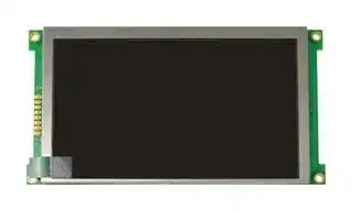
LMT050DNCFWU-NYN-1
TFT LCD, 5 ", 800 x 480 Pixels, Landscape, Black on White, 3.3V
⚠️ Reference pricing provided. In case of supply shortages, we will connect you with our trusted procurement partners to ensure your project's continuity.
- Manufacturer: INTELLIGENT DISPLAY SOLUTIONS
- Product type: TFT LCD Displays
- SVHC: No SVHC (25-Jun-2025)
- VGA Size: -
- Resolution: 800 x 480 Pixels
- Module Size: 136mm x 76mm x 10.3mm
- Touchscreen: -
- Display Size: 5"
- Logic Voltage: 3.3V
- Product Range: -
- Display Pinout: 26 Way Connector
- Interface Type: MCU
- Display Appearance: Black on White
- Display Brightness: 250cd/m²
- Display Orientation: Landscape
- Operating Temperature Max: 70°C
- Operating Temperature Min: -20°C
| Delivery and price | |
|---|---|
| Units per pack | 50 |
| Price | 46.26 € |
| Current stock | 10+ |
| Lead time | 30 days |
Datasheet

## **LMT050DNCFWU-NYN-1** LCD Module User Manual |||Prepared by:<br>**ChenYuming**|Checked by:|Approved by:<br>DingXin||| |---|---|---|---|---|---|---| |||||||| |**Rev.**|**Descriptions**||||**Release Date**|| |0.1|Preliminary||||2022-08-16|| |0.2|Updata Outline Drawing||||2023-04-13|| Intelligent Display Solutions, Unit 2, Berkshire Business Centre, Berkshire Drive, Thatcham, Berkshire, RG19 4EW Telephone : +44 (0)1635 294600 Fax : +44 (0)1635 869200 Email: info@i-lcd.com www.i-lcd.com A division of Intelligent Group Solutions Ltd Page: 1 of 13 LCD Module User Manual LMT050DNCFWU-NYN-1 ## **Table of Content** |**1.**|**General Specification ............................................................................................................ 3**| |---|---| |**2.**|**Block Diagram ........................................................................................................................ 3**| |**3.**|**Terminal Functions ................................................................................................................ 4**| |3.1|Interface ............................................................................................................................... 4| |**4.**|**Absolute Maximum Ratings .................................................................................................. 4**| |**5.**|**Electrical Characteristics ...................................................................................................... 4**| |5.1|DC Characteristics (MCU terminal)....................................................................................... 4| |**6.**|**8080 Characteristics .............................................................................................................. 5**| |6.1|Indirect 8-bit Timing ............................................................................................................. 5| |6.2|TFT Controller Reset Timing ................................................................................................ 6| |**7.**|**Commands ............................................................................................................................. 6**| |7.1|Command Summary ............................................................................................................ 6| |**8.**|**Optical Characteristics .......................................................................................................... 9**| |**9.**|**LCD Module Design and Handling Precautions ................................................................. 10**| |**10. **|**Outline Drawing ................................................................................................................... 13**| Intelligent Display Solutions, Unit 2, Berkshire Business Centre, Berkshire Drive, Thatcham, Berkshire, RG19 4EW Telephone : +44 (0)1635 294600 Fax : +44 (0)1635 869200 Email: info@i-lcd.com www.i-lcd.com A division of Intelligent Group Solutions Ltd Page: 2 of 13 LCD Module User Manual LMT050DNCFWU-NYN-1 ## **1. General Specification** Screen Size(Diagonal) : 5.0” Active Area : 108 x 64.8 (mm) Number of dots : 800 (RGB) x 480 Pixel Pitch : 0.135x0.135(mm) Color Depth: 256 color Display Technology : a-Si TFT active matrix Display Mode : Normal White, Transmissive Display Interface : MCU_8 bits Viewing Direction : 6 o’clock(Gray scale Inversion) (*1) 12 o’clock (*2) Operating Temperature : -20 ~ +70°C Storage Temperature : -30 ~ +80°C Note: - *1 Color tune may slightly changed by temperature and driving voltage. - *2. For saturated color display content (eg. pure-red, pure-green, pure-blue, or pure-colors-combinations) - *3. For "color scales" display content ## **2. Block Diagram** Intelligent Display Solutions, Unit 2, Berkshire Business Centre, Berkshire Drive, Thatcham, Berkshire, RG19 4EW Telephone : +44 (0)1635 294600 Fax : +44 (0)1635 869200 Email: info@i-lcd.com www.i-lcd.com A division of Intelligent Group Solutions Ltd Page: 3 of 13 LCD Module User Manual LMT050DNCFWU-NYN-1 ## **3. Terminal Functions** ## **3.1 Interface** **==> picture [495 x 419] intentionally omitted <==** **----- Start of picture text -----**<br> K3 Pin No. Pin Name I/O Descriptions Note<br>1~2 VSS P Power Ground<br>3~4 VDD P Positive Power Supply<br>Register Select<br>RS = H, status read/command write<br>5 RS I cycle is selected.<br>RS = L, data Read/Write cycle is<br>selected.<br>Chip Select<br>/CS=L, enable access to the LCD<br>6 /CS I interface<br>/CS=H, disable access to the LCD<br>interface<br>Reset signal<br>7 /RST I /RST = L, Initialization is executed<br>/RST = H, Normal running.<br>8~15 DB0~DB7 I Data Input<br>16 TE O TE Signal<br>17 NC -- No Connection<br>/WR=LH, RD=H;<br>18 /WR I Data or Instruction latch into the LCD<br>module<br>19 VSS P Power Ground<br>/WR=H, /RD=L;<br>20 /RD I Data or Status read form the LCD<br>module<br>21~26 NC -- No Connection<br>**----- End of picture text -----**<br> ## **4. Absolute Maximum Ratings** |**Items**<br>**Symbol**<br>**Min.**<br>**Max.**<br>**Unit**<br>**Condition**|**Items**<br>**Symbol**<br>**Min.**<br>**Max.**<br>**Unit**<br>**Condition**|**Items**<br>**Symbol**<br>**Min.**<br>**Max.**<br>**Unit**<br>**Condition**|**Items**<br>**Symbol**<br>**Min.**<br>**Max.**<br>**Unit**<br>**Condition**|**Items**<br>**Symbol**<br>**Min.**<br>**Max.**<br>**Unit**<br>**Condition**|**Items**<br>**Symbol**<br>**Min.**<br>**Max.**<br>**Unit**<br>**Condition**| |---|---|---|---|---|---| |Supply Voltage<br>VDD<br>-0.3<br>+3.6<br>V<br>Vss = 0V|||||| |OperatingTemperature<br>TOP<br>-20<br>+70<br>C<br>No Condensation|||||| |Storage Temperature|TST|-30|+80|C|No Condensation| Cautions: Any Stresses exceeding the Absolute Maximum Ratings may cause substantial damage to the device. Functional operation of this device at other conditions beyond those listed in the specification is not implied and prolonged exposure to extreme conditions may affect device reliability. Intelligent Display Solutions, Unit 2, Berkshire Business Centre, Berkshire Drive, Thatcham, Berkshire, RG19 4EW Telephone : +44 (0)1635 294600 Fax : +44 (0)1635 869200 Email: info@i-lcd.com www.i-lcd.com A division of Intelligent Group Solutions Ltd Page: 4 of 13 LCD Module User Manual LMT050DNCFWU-NYN-1 |Output Signal Low Voltage<br>VOL<br>--<br>--<br>VSS+0.4<br>V|Output Signal Low Voltage<br>VOL<br>--<br>--<br>VSS+0.4<br>V|Output Signal Low Voltage<br>VOL<br>--<br>--<br>VSS+0.4<br>V|Output Signal Low Voltage<br>VOL<br>--<br>--<br>VSS+0.4<br>V|Output Signal Low Voltage<br>VOL<br>--<br>--<br>VSS+0.4<br>V|Output Signal Low Voltage<br>VOL<br>--<br>--<br>VSS+0.4<br>V| |---|---|---|---|---|---| |Operating Current<br>IDD<br>-<br>TBD<br>-<br>mA<br>All black, Backlight ON<br>-<br>TBD<br>-<br>mA<br>All black,Backlight OFF|||||| ||-|TBD|-|mA|All black,Backlight OFF| ## **6. 8080 Characteristics** ## **6.1 Indirect 8-bit Timing** Note:Refer to the S1D13L01 datasheet for more details Intelligent Display Solutions, Unit 2, Berkshire Business Centre, Berkshire Drive, Thatcham, Berkshire, RG19 4EW Telephone : +44 (0)1635 294600 Fax : +44 (0)1635 869200 Email: info@i-lcd.com www.i-lcd.com A division of Intelligent Group Solutions Ltd Page: 5 of 13 LCD Module User Manual LMT050DNCFWU-NYN-1 ## **6.2 TFT Controller Reset Timing** VSS=0V, VDD=3.3V, TOP=25C **Symbol Parameter MIN. MAX. Unit** t1 Reset Pulse Width is ignored - 42 ns ~~ree~~ t2 Active Reset Pulse Width (see Note) 150 - ns Note:The RESET# line should be held low longer than 150ns to guarantee reset. ## **7. Commands** **7.1 Command Summary** |**Command**<br>**Para-**<br>**meter**<br>**HEX**<br>**A0**<br>**/CS**<br>**/WR**<br>**D7**<br>**D6**<br>**D5**<br>**D4**<br>**D3**<br>**D2**<br>**D1**<br>**D0**<br>**Descriptions**<br>Power Save<br>P1<br>60804<br>0<br>0<br>0<br>A[7:0]-> A[15:8] -> A[18:16]<br>Power Save Configuration Register<br>P2<br>D[7:0]<br>1<br>0<br>0<br>n/a<br>n/a<br>n/a<br>n/a<br>n/a<br>n/a<br>Power Save Bit[1:0] = 00 , PSM0 mode<br>Bit[1:0] = 01 , PSM1 mode<br>Bit[1:0]= 1x,NMM mode<br>D[15:8]<br>1<br>0<br>0<br>n/a<br>n/a<br>n/a<br>n/a<br>n/a<br>n/a<br>n/a<br>n/a<br>Software<br>Reset<br>P1<br>60806<br>0<br>0<br>0<br>A[7:0]-> A[15:8] -> A[18:16]<br>Software Reset Register(Write Only)<br>P2<br>D[7:0]<br>1<br>0<br>0<br>n/a<br>n/a<br>n/a<br>n/a<br>n/a<br>n/a<br>n/a<br>n/a<br>Bit[8] = 0 , no effect in hardware<br>Bit[8] = 1 , all registers are reset to default values<br>D[15:8]<br>1<br>0<br>0<br>n/a<br>n/a<br>n/a<br>n/a<br>n/a<br>n/a<br>n/a<br>Softw<br>are<br>Reset<br>PLL Setting 0<br>P1<br>60810<br>0<br>0<br>0<br>A[7:0]-> A[15:8] -> A[18:16]<br>PLL SettingRegister 0<br>P2<br>D[7:0]<br>1<br>0<br>0<br>n/a<br>n/a<br>n/a<br>n/a<br>n/a<br>n/a<br>PLL<br>Bypa<br>ss<br>PLL<br>Enabl<br>e<br>Bit[0] = 0 , the PLL is disabled<br>Bit[0] = 1 , the PLL enabled<br>Bit[1] = 0 , PLL is selected<br>Bit[1] = 1 , CLKI is selected<br>Bit[15] = 0 , the PLL output is not stable<br>Bit[15]= 1,the PLL output is stable<br>D[15:8]<br>1<br>0<br>0<br>PLL<br>Lock<br>(RO)<br>n/a<br>n/a<br>n/a<br>n/a<br>n/a<br>n/a<br>n/a<br>PLL Setting 1<br>P1<br>60812<br>0<br>0<br>0<br>A[7:0]-> A[15:8] -> A[18:16]<br>PLL SettingRegister 1<br>P2<br>D[7:0]<br>1<br>0<br>0<br>M-Divider<br>Bit[9:0] 000h,001h … … 019h,020h : 1:1 ,2:1 … … 33:1(M-Divide Ratio).<br>021h to 13Fh: Reserved, PFDCLK = CLKI ÷ (M-Divider + 1)<br>Bit[13:10] , must be set to 0000<br>D[15:8]<br>1<br>0<br>0<br>n/a<br>n/a<br>N-Counter<br>M-Divider<br>~~Lo~~<br>~~PR PE~~<br>~~A~~<br>~~TH~~<br>~~POR~~|**Command**<br>**Para-**<br>**meter**<br>**HEX**<br>**A0**<br>**/CS**<br>**/WR**<br>**D7**<br>**D6**<br>**D5**<br>**D4**<br>**D3**<br>**D2**<br>**D1**<br>**D0**<br>**Descriptions**<br>Power Save<br>P1<br>60804<br>0<br>0<br>0<br>A[7:0]-> A[15:8] -> A[18:16]<br>Power Save Configuration Register<br>P2<br>D[7:0]<br>1<br>0<br>0<br>n/a<br>n/a<br>n/a<br>n/a<br>n/a<br>n/a<br>Power Save Bit[1:0] = 00 , PSM0 mode<br>Bit[1:0] = 01 , PSM1 mode<br>Bit[1:0]= 1x,NMM mode<br>D[15:8]<br>1<br>0<br>0<br>n/a<br>n/a<br>n/a<br>n/a<br>n/a<br>n/a<br>n/a<br>n/a<br>Software<br>Reset<br>P1<br>60806<br>0<br>0<br>0<br>A[7:0]-> A[15:8] -> A[18:16]<br>Software Reset Register(Write Only)<br>P2<br>D[7:0]<br>1<br>0<br>0<br>n/a<br>n/a<br>n/a<br>n/a<br>n/a<br>n/a<br>n/a<br>n/a<br>Bit[8] = 0 , no effect in hardware<br>Bit[8] = 1 , all registers are reset to default values<br>D[15:8]<br>1<br>0<br>0<br>n/a<br>n/a<br>n/a<br>n/a<br>n/a<br>n/a<br>n/a<br>Softw<br>are<br>Reset<br>PLL Setting 0<br>P1<br>60810<br>0<br>0<br>0<br>A[7:0]-> A[15:8] -> A[18:16]<br>PLL SettingRegister 0<br>P2<br>D[7:0]<br>1<br>0<br>0<br>n/a<br>n/a<br>n/a<br>n/a<br>n/a<br>n/a<br>PLL<br>Bypa<br>ss<br>PLL<br>Enabl<br>e<br>Bit[0] = 0 , the PLL is disabled<br>Bit[0] = 1 , the PLL enabled<br>Bit[1] = 0 , PLL is selected<br>Bit[1] = 1 , CLKI is selected<br>Bit[15] = 0 , the PLL output is not stable<br>Bit[15]= 1,the PLL output is stable<br>D[15:8]<br>1<br>0<br>0<br>PLL<br>Lock<br>(RO)<br>n/a<br>n/a<br>n/a<br>n/a<br>n/a<br>n/a<br>n/a<br>PLL Setting 1<br>P1<br>60812<br>0<br>0<br>0<br>A[7:0]-> A[15:8] -> A[18:16]<br>PLL SettingRegister 1<br>P2<br>D[7:0]<br>1<br>0<br>0<br>M-Divider<br>Bit[9:0] 000h,001h … … 019h,020h : 1:1 ,2:1 … … 33:1(M-Divide Ratio).<br>021h to 13Fh: Reserved, PFDCLK = CLKI ÷ (M-Divider + 1)<br>Bit[13:10] , must be set to 0000<br>D[15:8]<br>1<br>0<br>0<br>n/a<br>n/a<br>N-Counter<br>M-Divider<br>~~Lo~~<br>~~PR PE~~<br>~~A~~<br>~~TH~~<br>~~POR~~|**Command**<br>**Para-**<br>**meter**<br>**HEX**<br>**A0**<br>**/CS**<br>**/WR**<br>**D7**<br>**D6**<br>**D5**<br>**D4**<br>**D3**<br>**D2**<br>**D1**<br>**D0**<br>**Descriptions**<br>Power Save<br>P1<br>60804<br>0<br>0<br>0<br>A[7:0]-> A[15:8] -> A[18:16]<br>Power Save Configuration Register<br>P2<br>D[7:0]<br>1<br>0<br>0<br>n/a<br>n/a<br>n/a<br>n/a<br>n/a<br>n/a<br>Power Save Bit[1:0] = 00 , PSM0 mode<br>Bit[1:0] = 01 , PSM1 mode<br>Bit[1:0]= 1x,NMM mode<br>D[15:8]<br>1<br>0<br>0<br>n/a<br>n/a<br>n/a<br>n/a<br>n/a<br>n/a<br>n/a<br>n/a<br>Software<br>Reset<br>P1<br>60806<br>0<br>0<br>0<br>A[7:0]-> A[15:8] -> A[18:16]<br>Software Reset Register(Write Only)<br>P2<br>D[7:0]<br>1<br>0<br>0<br>n/a<br>n/a<br>n/a<br>n/a<br>n/a<br>n/a<br>n/a<br>n/a<br>Bit[8] = 0 , no effect in hardware<br>Bit[8] = 1 , all registers are reset to default values<br>D[15:8]<br>1<br>0<br>0<br>n/a<br>n/a<br>n/a<br>n/a<br>n/a<br>n/a<br>n/a<br>Softw<br>are<br>Reset<br>PLL Setting 0<br>P1<br>60810<br>0<br>0<br>0<br>A[7:0]-> A[15:8] -> A[18:16]<br>PLL SettingRegister 0<br>P2<br>D[7:0]<br>1<br>0<br>0<br>n/a<br>n/a<br>n/a<br>n/a<br>n/a<br>n/a<br>PLL<br>Bypa<br>ss<br>PLL<br>Enabl<br>e<br>Bit[0] = 0 , the PLL is disabled<br>Bit[0] = 1 , the PLL enabled<br>Bit[1] = 0 , PLL is selected<br>Bit[1] = 1 , CLKI is selected<br>Bit[15] = 0 , the PLL output is not stable<br>Bit[15]= 1,the PLL output is stable<br>D[15:8]<br>1<br>0<br>0<br>PLL<br>Lock<br>(RO)<br>n/a<br>n/a<br>n/a<br>n/a<br>n/a<br>n/a<br>n/a<br>PLL Setting 1<br>P1<br>60812<br>0<br>0<br>0<br>A[7:0]-> A[15:8] -> A[18:16]<br>PLL SettingRegister 1<br>P2<br>D[7:0]<br>1<br>0<br>0<br>M-Divider<br>Bit[9:0] 000h,001h … … 019h,020h : 1:1 ,2:1 … … 33:1(M-Divide Ratio).<br>021h to 13Fh: Reserved, PFDCLK = CLKI ÷ (M-Divider + 1)<br>Bit[13:10] , must be set to 0000<br>D[15:8]<br>1<br>0<br>0<br>n/a<br>n/a<br>N-Counter<br>M-Divider<br>~~Lo~~<br>~~PR PE~~<br>~~A~~<br>~~TH~~<br>~~POR~~|**Command**<br>**Para-**<br>**meter**<br>**HEX**<br>**A0**<br>**/CS**<br>**/WR**<br>**D7**<br>**D6**<br>**D5**<br>**D4**<br>**D3**<br>**D2**<br>**D1**<br>**D0**<br>**Descriptions**<br>Power Save<br>P1<br>60804<br>0<br>0<br>0<br>A[7:0]-> A[15:8] -> A[18:16]<br>Power Save Configuration Register<br>P2<br>D[7:0]<br>1<br>0<br>0<br>n/a<br>n/a<br>n/a<br>n/a<br>n/a<br>n/a<br>Power Save Bit[1:0] = 00 , PSM0 mode<br>Bit[1:0] = 01 , PSM1 mode<br>Bit[1:0]= 1x,NMM mode<br>D[15:8]<br>1<br>0<br>0<br>n/a<br>n/a<br>n/a<br>n/a<br>n/a<br>n/a<br>n/a<br>n/a<br>Software<br>Reset<br>P1<br>60806<br>0<br>0<br>0<br>A[7:0]-> A[15:8] -> A[18:16]<br>Software Reset Register(Write Only)<br>P2<br>D[7:0]<br>1<br>0<br>0<br>n/a<br>n/a<br>n/a<br>n/a<br>n/a<br>n/a<br>n/a<br>n/a<br>Bit[8] = 0 , no effect in hardware<br>Bit[8] = 1 , all registers are reset to default values<br>D[15:8]<br>1<br>0<br>0<br>n/a<br>n/a<br>n/a<br>n/a<br>n/a<br>n/a<br>n/a<br>Softw<br>are<br>Reset<br>PLL Setting 0<br>P1<br>60810<br>0<br>0<br>0<br>A[7:0]-> A[15:8] -> A[18:16]<br>PLL SettingRegister 0<br>P2<br>D[7:0]<br>1<br>0<br>0<br>n/a<br>n/a<br>n/a<br>n/a<br>n/a<br>n/a<br>PLL<br>Bypa<br>ss<br>PLL<br>Enabl<br>e<br>Bit[0] = 0 , the PLL is disabled<br>Bit[0] = 1 , the PLL enabled<br>Bit[1] = 0 , PLL is selected<br>Bit[1] = 1 , CLKI is selected<br>Bit[15] = 0 , the PLL output is not stable<br>Bit[15]= 1,the PLL output is stable<br>D[15:8]<br>1<br>0<br>0<br>PLL<br>Lock<br>(RO)<br>n/a<br>n/a<br>n/a<br>n/a<br>n/a<br>n/a<br>n/a<br>PLL Setting 1<br>P1<br>60812<br>0<br>0<br>0<br>A[7:0]-> A[15:8] -> A[18:16]<br>PLL SettingRegister 1<br>P2<br>D[7:0]<br>1<br>0<br>0<br>M-Divider<br>Bit[9:0] 000h,001h … … 019h,020h : 1:1 ,2:1 … … 33:1(M-Divide Ratio).<br>021h to 13Fh: Reserved, PFDCLK = CLKI ÷ (M-Divider + 1)<br>Bit[13:10] , must be set to 0000<br>D[15:8]<br>1<br>0<br>0<br>n/a<br>n/a<br>N-Counter<br>M-Divider<br>~~Lo~~<br>~~PR PE~~<br>~~A~~<br>~~TH~~<br>~~POR~~|**Command**<br>**Para-**<br>**meter**<br>**HEX**<br>**A0**<br>**/CS**<br>**/WR**<br>**D7**<br>**D6**<br>**D5**<br>**D4**<br>**D3**<br>**D2**<br>**D1**<br>**D0**<br>**Descriptions**<br>Power Save<br>P1<br>60804<br>0<br>0<br>0<br>A[7:0]-> A[15:8] -> A[18:16]<br>Power Save Configuration Register<br>P2<br>D[7:0]<br>1<br>0<br>0<br>n/a<br>n/a<br>n/a<br>n/a<br>n/a<br>n/a<br>Power Save Bit[1:0] = 00 , PSM0 mode<br>Bit[1:0] = 01 , PSM1 mode<br>Bit[1:0]= 1x,NMM mode<br>D[15:8]<br>1<br>0<br>0<br>n/a<br>n/a<br>n/a<br>n/a<br>n/a<br>n/a<br>n/a<br>n/a<br>Software<br>Reset<br>P1<br>60806<br>0<br>0<br>0<br>A[7:0]-> A[15:8] -> A[18:16]<br>Software Reset Register(Write Only)<br>P2<br>D[7:0]<br>1<br>0<br>0<br>n/a<br>n/a<br>n/a<br>n/a<br>n/a<br>n/a<br>n/a<br>n/a<br>Bit[8] = 0 , no effect in hardware<br>Bit[8] = 1 , all registers are reset to default values<br>D[15:8]<br>1<br>0<br>0<br>n/a<br>n/a<br>n/a<br>n/a<br>n/a<br>n/a<br>n/a<br>Softw<br>are<br>Reset<br>PLL Setting 0<br>P1<br>60810<br>0<br>0<br>0<br>A[7:0]-> A[15:8] -> A[18:16]<br>PLL SettingRegister 0<br>P2<br>D[7:0]<br>1<br>0<br>0<br>n/a<br>n/a<br>n/a<br>n/a<br>n/a<br>n/a<br>PLL<br>Bypa<br>ss<br>PLL<br>Enabl<br>e<br>Bit[0] = 0 , the PLL is disabled<br>Bit[0] = 1 , the PLL enabled<br>Bit[1] = 0 , PLL is selected<br>Bit[1] = 1 , CLKI is selected<br>Bit[15] = 0 , the PLL output is not stable<br>Bit[15]= 1,the PLL output is stable<br>D[15:8]<br>1<br>0<br>0<br>PLL<br>Lock<br>(RO)<br>n/a<br>n/a<br>n/a<br>n/a<br>n/a<br>n/a<br>n/a<br>PLL Setting 1<br>P1<br>60812<br>0<br>0<br>0<br>A[7:0]-> A[15:8] -> A[18:16]<br>PLL SettingRegister 1<br>P2<br>D[7:0]<br>1<br>0<br>0<br>M-Divider<br>Bit[9:0] 000h,001h … … 019h,020h : 1:1 ,2:1 … … 33:1(M-Divide Ratio).<br>021h to 13Fh: Reserved, PFDCLK = CLKI ÷ (M-Divider + 1)<br>Bit[13:10] , must be set to 0000<br>D[15:8]<br>1<br>0<br>0<br>n/a<br>n/a<br>N-Counter<br>M-Divider<br>~~Lo~~<br>~~PR PE~~<br>~~A~~<br>~~TH~~<br>~~POR~~|**Command**<br>**Para-**<br>**meter**<br>**HEX**<br>**A0**<br>**/CS**<br>**/WR**<br>**D7**<br>**D6**<br>**D5**<br>**D4**<br>**D3**<br>**D2**<br>**D1**<br>**D0**<br>**Descriptions**<br>Power Save<br>P1<br>60804<br>0<br>0<br>0<br>A[7:0]-> A[15:8] -> A[18:16]<br>Power Save Configuration Register<br>P2<br>D[7:0]<br>1<br>0<br>0<br>n/a<br>n/a<br>n/a<br>n/a<br>n/a<br>n/a<br>Power Save Bit[1:0] = 00 , PSM0 mode<br>Bit[1:0] = 01 , PSM1 mode<br>Bit[1:0]= 1x,NMM mode<br>D[15:8]<br>1<br>0<br>0<br>n/a<br>n/a<br>n/a<br>n/a<br>n/a<br>n/a<br>n/a<br>n/a<br>Software<br>Reset<br>P1<br>60806<br>0<br>0<br>0<br>A[7:0]-> A[15:8] -> A[18:16]<br>Software Reset Register(Write Only)<br>P2<br>D[7:0]<br>1<br>0<br>0<br>n/a<br>n/a<br>n/a<br>n/a<br>n/a<br>n/a<br>n/a<br>n/a<br>Bit[8] = 0 , no effect in hardware<br>Bit[8] = 1 , all registers are reset to default values<br>D[15:8]<br>1<br>0<br>0<br>n/a<br>n/a<br>n/a<br>n/a<br>n/a<br>n/a<br>n/a<br>Softw<br>are<br>Reset<br>PLL Setting 0<br>P1<br>60810<br>0<br>0<br>0<br>A[7:0]-> A[15:8] -> A[18:16]<br>PLL SettingRegister 0<br>P2<br>D[7:0]<br>1<br>0<br>0<br>n/a<br>n/a<br>n/a<br>n/a<br>n/a<br>n/a<br>PLL<br>Bypa<br>ss<br>PLL<br>Enabl<br>e<br>Bit[0] = 0 , the PLL is disabled<br>Bit[0] = 1 , the PLL enabled<br>Bit[1] = 0 , PLL is selected<br>Bit[1] = 1 , CLKI is selected<br>Bit[15] = 0 , the PLL output is not stable<br>Bit[15]= 1,the PLL output is stable<br>D[15:8]<br>1<br>0<br>0<br>PLL<br>Lock<br>(RO)<br>n/a<br>n/a<br>n/a<br>n/a<br>n/a<br>n/a<br>n/a<br>PLL Setting 1<br>P1<br>60812<br>0<br>0<br>0<br>A[7:0]-> A[15:8] -> A[18:16]<br>PLL SettingRegister 1<br>P2<br>D[7:0]<br>1<br>0<br>0<br>M-Divider<br>Bit[9:0] 000h,001h … … 019h,020h : 1:1 ,2:1 … … 33:1(M-Divide Ratio).<br>021h to 13Fh: Reserved, PFDCLK = CLKI ÷ (M-Divider + 1)<br>Bit[13:10] , must be set to 0000<br>D[15:8]<br>1<br>0<br>0<br>n/a<br>n/a<br>N-Counter<br>M-Divider<br>~~Lo~~<br>~~PR PE~~<br>~~A~~<br>~~TH~~<br>~~POR~~|**Command**<br>**Para-**<br>**meter**<br>**HEX**<br>**A0**<br>**/CS**<br>**/WR**<br>**D7**<br>**D6**<br>**D5**<br>**D4**<br>**D3**<br>**D2**<br>**D1**<br>**D0**<br>**Descriptions**<br>Power Save<br>P1<br>60804<br>0<br>0<br>0<br>A[7:0]-> A[15:8] -> A[18:16]<br>Power Save Configuration Register<br>P2<br>D[7:0]<br>1<br>0<br>0<br>n/a<br>n/a<br>n/a<br>n/a<br>n/a<br>n/a<br>Power Save Bit[1:0] = 00 , PSM0 mode<br>Bit[1:0] = 01 , PSM1 mode<br>Bit[1:0]= 1x,NMM mode<br>D[15:8]<br>1<br>0<br>0<br>n/a<br>n/a<br>n/a<br>n/a<br>n/a<br>n/a<br>n/a<br>n/a<br>Software<br>Reset<br>P1<br>60806<br>0<br>0<br>0<br>A[7:0]-> A[15:8] -> A[18:16]<br>Software Reset Register(Write Only)<br>P2<br>D[7:0]<br>1<br>0<br>0<br>n/a<br>n/a<br>n/a<br>n/a<br>n/a<br>n/a<br>n/a<br>n/a<br>Bit[8] = 0 , no effect in hardware<br>Bit[8] = 1 , all registers are reset to default values<br>D[15:8]<br>1<br>0<br>0<br>n/a<br>n/a<br>n/a<br>n/a<br>n/a<br>n/a<br>n/a<br>Softw<br>are<br>Reset<br>PLL Setting 0<br>P1<br>60810<br>0<br>0<br>0<br>A[7:0]-> A[15:8] -> A[18:16]<br>PLL SettingRegister 0<br>P2<br>D[7:0]<br>1<br>0<br>0<br>n/a<br>n/a<br>n/a<br>n/a<br>n/a<br>n/a<br>PLL<br>Bypa<br>ss<br>PLL<br>Enabl<br>e<br>Bit[0] = 0 , the PLL is disabled<br>Bit[0] = 1 , the PLL enabled<br>Bit[1] = 0 , PLL is selected<br>Bit[1] = 1 , CLKI is selected<br>Bit[15] = 0 , the PLL output is not stable<br>Bit[15]= 1,the PLL output is stable<br>D[15:8]<br>1<br>0<br>0<br>PLL<br>Lock<br>(RO)<br>n/a<br>n/a<br>n/a<br>n/a<br>n/a<br>n/a<br>n/a<br>PLL Setting 1<br>P1<br>60812<br>0<br>0<br>0<br>A[7:0]-> A[15:8] -> A[18:16]<br>PLL SettingRegister 1<br>P2<br>D[7:0]<br>1<br>0<br>0<br>M-Divider<br>Bit[9:0] 000h,001h … … 019h,020h : 1:1 ,2:1 … … 33:1(M-Divide Ratio).<br>021h to 13Fh: Reserved, PFDCLK = CLKI ÷ (M-Divider + 1)<br>Bit[13:10] , must be set to 0000<br>D[15:8]<br>1<br>0<br>0<br>n/a<br>n/a<br>N-Counter<br>M-Divider<br>~~Lo~~<br>~~PR PE~~<br>~~A~~<br>~~TH~~<br>~~POR~~|**Command**<br>**Para-**<br>**meter**<br>**HEX**<br>**A0**<br>**/CS**<br>**/WR**<br>**D7**<br>**D6**<br>**D5**<br>**D4**<br>**D3**<br>**D2**<br>**D1**<br>**D0**<br>**Descriptions**<br>Power Save<br>P1<br>60804<br>0<br>0<br>0<br>A[7:0]-> A[15:8] -> A[18:16]<br>Power Save Configuration Register<br>P2<br>D[7:0]<br>1<br>0<br>0<br>n/a<br>n/a<br>n/a<br>n/a<br>n/a<br>n/a<br>Power Save Bit[1:0] = 00 , PSM0 mode<br>Bit[1:0] = 01 , PSM1 mode<br>Bit[1:0]= 1x,NMM mode<br>D[15:8]<br>1<br>0<br>0<br>n/a<br>n/a<br>n/a<br>n/a<br>n/a<br>n/a<br>n/a<br>n/a<br>Software<br>Reset<br>P1<br>60806<br>0<br>0<br>0<br>A[7:0]-> A[15:8] -> A[18:16]<br>Software Reset Register(Write Only)<br>P2<br>D[7:0]<br>1<br>0<br>0<br>n/a<br>n/a<br>n/a<br>n/a<br>n/a<br>n/a<br>n/a<br>n/a<br>Bit[8] = 0 , no effect in hardware<br>Bit[8] = 1 , all registers are reset to default values<br>D[15:8]<br>1<br>0<br>0<br>n/a<br>n/a<br>n/a<br>n/a<br>n/a<br>n/a<br>n/a<br>Softw<br>are<br>Reset<br>PLL Setting 0<br>P1<br>60810<br>0<br>0<br>0<br>A[7:0]-> A[15:8] -> A[18:16]<br>PLL SettingRegister 0<br>P2<br>D[7:0]<br>1<br>0<br>0<br>n/a<br>n/a<br>n/a<br>n/a<br>n/a<br>n/a<br>PLL<br>Bypa<br>ss<br>PLL<br>Enabl<br>e<br>Bit[0] = 0 , the PLL is disabled<br>Bit[0] = 1 , the PLL enabled<br>Bit[1] = 0 , PLL is selected<br>Bit[1] = 1 , CLKI is selected<br>Bit[15] = 0 , the PLL output is not stable<br>Bit[15]= 1,the PLL output is stable<br>D[15:8]<br>1<br>0<br>0<br>PLL<br>Lock<br>(RO)<br>n/a<br>n/a<br>n/a<br>n/a<br>n/a<br>n/a<br>n/a<br>PLL Setting 1<br>P1<br>60812<br>0<br>0<br>0<br>A[7:0]-> A[15:8] -> A[18:16]<br>PLL SettingRegister 1<br>P2<br>D[7:0]<br>1<br>0<br>0<br>M-Divider<br>Bit[9:0] 000h,001h … … 019h,020h : 1:1 ,2:1 … … 33:1(M-Divide Ratio).<br>021h to 13Fh: Reserved, PFDCLK = CLKI ÷ (M-Divider + 1)<br>Bit[13:10] , must be set to 0000<br>D[15:8]<br>1<br>0<br>0<br>n/a<br>n/a<br>N-Counter<br>M-Divider<br>~~Lo~~<br>~~PR PE~~<br>~~A~~<br>~~TH~~<br>~~POR~~| |---|---|---|---|---|---|---|---| |PLL Setting 2<br>P1<br>60814<br>0|0|0|||A[7:0]-> A[15:8] -> A[18:16]||PLL SettingRegister 2| |P2<br>D[7:0]<br>1<br>D[15:8]<br>1|0<br>0|0<br>0|n/a|n/a|n/a|L-Counter<br>n/a<br>n/a<br>n/a<br>L-Counter|Bit[9:0] , must be set between 010h ~ 041h. , and get the M-Divide Ratio<br>from 17:1 to 66:1. POCLK = (L-Counter + 1) x (N-Counter + 1) x PFDCLK| |Internal Clock<br>P1<br>60816<br>0|0|0|||A[7:0]-> A[15:8] -> A[18:16]||Internal Clock Configuration Register| |Configuration<br>P2<br>D[7:0]<br>1<br>D[15:8]<br>1|0<br>0|0<br>0|n/a<br>n/a|n/a<br>n/a|n/a<br>n/a|n/a<br>n/a<br>PCLK Divide Select <br>n/a<br>n/a<br>n/a<br>n/a<br>n/a|Bit[3:0] = 0000b,0001b … … 1110b,1111b : 1:1 ,2:1 … … 16:1(MCLK to<br>PCLK Frequency Ratio)| |Panel Setting<br>P1<br>60820<br>0|0|0|||A[7:0]-> A[15:8] -> A[18:16]||Panel SettingMiscellaneous Register| |Miscellaneous<br>D[7:0]<br>1|0|0|DE Polarity||PCLK<br>Polari<br>ty|PCLK<br>n/a<br>Panel<br>Data<br>Enabl<br>e<br>Panel Data<br>Width<br>Panel<br>Port<br>Enabl<br>e|el<br>Bit[0] = 0 , TFT panel is disable<br>Bit[0] = 1 , TFT panel is enable<br>Bit[2:1] = 01 , TFT 16-bit<br>Bit[2:1] = 10 , TFT 18-bit| |P2<br>D[15:8]<br>1|0|0|n/a|n/a|n/a|n/a<br>n/a<br>n/a<br>n/a<br>n/a|Bit[2:1] = 11 , TFT 24-bit<br>Bit[3] = 0 , panel data is disable<br>Bit[3] = 1 , panel data is enable<br>Bit[5] = 0, the LCD data outputs transition on the rising edge of PCLK<br>Bit[5] = 1 , the LCD data outputs transition on the falling edge of PCLK<br>Bit[7:6] = 00 , DE Polarity Low active<br>Bit[7:6] = 01 , DE Polarity High active<br>Bit[7:6] = 10 , DE Polarity Fixed to Low<br>Bit[7:6]= 11,DE PolarityFixed to High| |Display<br>P1<br>60822<br>0|0|0|||A[7:0]-> A[15:8] -> A[18:16]||DisplaySettings Register| Intelligent Display Solutions, Unit 2, Berkshire Business Centre, Berkshire Drive, Thatcham, Berkshire, RG19 4EW Telephone : +44 (0)1635 294600 Fax : +44 (0)1635 869200 Email: info@i-lcd.com www.i-lcd.com A division of Intelligent Group Solutions Ltd Page: 6 of 13 LCD Module User Manual LMT050DNCFWU-NYN-1 **==> picture [495 x 285] intentionally omitted <==** **----- Start of picture text -----**<br> Settings D[7:0] TE Displ Panel Bit[0] = 0 , HS, VS, DE and PCLK are fixed to H or L and the display pipes<br>Statu Displ ay SW Interf are disabled<br>1 0 0 s TE Function Blankay n/a PolariBlank Video Invert Enablace Bit[0] = 1 , enable the panel output and display pipes Bit[1] = 0 , video data is normal<br>(RO) ty es Bit[1] = 1 , video data is inverted<br>D[15:8] Bit[2] = 0 , the display blank function operates normally<br>Bit[2] = 1 , the display blank function switches polarity<br>Bit[4] = 0 , the LCD data is masked<br>Bit[4] = 1 , all applicable LCD data outputs are forced to zero or one<br>P2 Bit[6:5] = 00b , TE output is disabled and the pin output is low<br>TE<br>Bit[6:5] = 01b , TE output is high (1) when the display is in the Vertical<br>Outp<br>Non-Display Period (VNDP) and low (0) when the display is in Vertical<br>1 0 0 n/a n/a n/a n/a n/a n/a n/a ut Pin<br>Display Period (VDISP)<br>Disab<br>Bit[6:5] = 10b , Line Count<br>le<br>Bit[6:5] = 11b , Reserved<br>Bit[7] = 0 , the selected condition in not occurring<br>Bit[7] = 1 , the selected condition in not occurring<br>Bit[8] = 0 , TE is output<br>Bit[8] = 1 , TE is not output<br>HDISP P1 60824 0 0 0 A[7:0]-> A[15:8] -> A[18:16] Horizontal Display Width Register (HDISP)<br>D[7:0] 1 0 0 n/a Horizontal Display Width<br>P2 Bit[6:0] = horizontal display width in pixels ÷ 8<br>D[15:8] 1 0 0 n/a n/a n/a n/a n/a n/a n/a n/a<br>HNDP P1 60826 0 0 0 A[7:0]-> A[15:8] -> A[18:16] Horizontal Non-Display Period Register (HNDP)<br>D[7:0] 1 0 0 n/a Horizontal Non-Display Period<br>P2 Bit[6:0] = horizontal non-display period in PCLK’s<br>D[15:8] 1 0 0 n/a n/a n/a n/a n/a n/a n/a n/a<br>VDISP P1 60828 0 0 0 A[7:0]-> A[15:8] -> A[18:16] Vertical Display Height Register (VDISP)<br>D[7:0] 1 0 0 Vertical Display Height<br>P2 D[15:8] Vertical Bit[9:0] = vertical display height in lines<br>1 0 0 n/a n/a n/a n/a n/a n/a Display<br>Height<br>VNDP P1 6082A 0 0 0 A[7:0]-> A[15:8] -> A[18:16] Vertical Non-Display Period Register (VNDP)<br>D[7:0] 1 0 0 Vertical Non-Display Period<br>P2 Bit[7:0] = vertical non-display period in lines<br>D[15:8] 1 0 0 n/a n/a n/a n/a n/a n/a n/a n/a<br>**----- End of picture text -----**<br> **==> picture [495 x 425] intentionally omitted <==** **----- Start of picture text -----**<br> Para-<br>Command HEX Descriptions<br>meter<br>HSW P1 6082C 0 0 0 A[7:0]-> A[15:8] -> A[18:16] HS Pulse Width Register (HSW)<br>D[7:0] HS<br>1 0 0 Pulse HS Pulse Width Bit[6:0] = HS pulse width in PCLK’s<br>P2 Polari Bit[7] = 0 , the horizontal sync signal is active low<br>ty Bit[7] = 1 , the horizontal sync signal is active high<br>D[15:8] 1 0 0 n/a n/a n/a n/a n/a n/a n/a n/a<br>HPS P1 6082E 0 0 0 A[7:0]-> A[15:8] -> A[18:16] HS Pulse Start Position Register (HPS)<br>D[7:0] 1 0 0 n/a HS Pulse Start Position<br>P2 Bit[6:0] = HS pulse start position in PCLK’s<br>D[15:8] 1 0 0 n/a n/a n/a n/a n/a n/a n/a n/a<br>VSW P1 60830 0 0 0 A[7:0]-> A[15:8] -> A[18:16] VS Pulse Width Register (VSW)<br>D[7:0] VS<br>1 0 0 Pulse n/a VS Pulse Width Bit[5:0] = VS pulse width in lines<br>P2 Polari Bit[7] = 0 , the vertical sync signal is active low<br>ty Bit[7] = 1 , the vertical sync signal is active high<br>D[15:8] 1 0 0 n/a n/a n/a n/a n/a n/a n/a n/a<br>VPS P1 60832 0 0 0 A[7:0]-> A[15:8] -> A[18:16] VS Pulse Start Position Register (VPS)<br>D[7:0] 1 0 0 VS Pulse Start Position<br>P2 Bit[7:0] = VS pulse start position in lines<br>D[15:8] 1 0 0 n/a n/a n/a n/a n/a n/a n/a n/a<br>TE Line Count P1 60834 0 0 0 A[7:0]-> A[15:8] -> A[18:16] TE Line Count Register<br>D[7:0] 1 0 0 TE Line Count<br>These bits specify the line count value that is compared with the internal<br>P2 D[15:8] 1 0 0 n/a n/a n/a n/a n/a n/a TE Line vertical line counter<br>Count<br>Main Layer P1 60840 0 0 0 A[7:0]-> A[15:8] -> A[18:16] Main Layer Setting Register<br>Setting D[7:0] 1 0 0 n/a n/a n/a Main Layer Rotation Main Layer Color<br>Select Depth Bit[2:0] = 000b, RGB 8:8:8 (default)<br>Bit[2:0] = 001b, RGB 5:6:5<br>D[15:8] Multi-<br>Bit[2:0] = 010b/011b/111b, Reserved<br>Byte<br>Bit[2:0] = 100b, 24 bpp + LUT1<br>Layer<br>Bit[2:0] = 101b, 16 bpp + LUT1<br>Regis<br>Bit[2:0] = 110b, 8 bpp + LUT1<br>P2 ters<br>Bit[4:3] = 00b, 0° (Normal)<br>1 0 0 n/a n/a n/a n/a n/a n/a n/a Sync Bit[4:3] = 01b, 90°<br>hrono<br>Bit[4:3] = 10b, 180°<br>us Bit[4:3] = 11b, 270°<br>Latch<br>Bit[8] = 0, Synchronous latching of multi-byte layer registers is enabled<br>ing<br>Bit[8] = 1, Synchronous latching of multi-byte layer registers is disabled<br>Disab<br>le<br>Main Layer P1 60842 0 0 0 A[7:0]-> A[15:8] -> A[18:16] Main Layer Start Address Register 0<br>Start Address D[7:0] 1 0 0 Main Layer Start Address Bit[15:0] is Bit[15:0] of Main Layer Start Address ,but Bit[1:0] must be set<br>P2<br>0 D[15:8] 1 0 0 Main Layer Start Address to 00b<br>Main Layer P1 60844 0 0 0 A[7:0]-> A[15:8] -> A[18:16] Main Layer Start Address Register 1<br>Start Address D[7:0] 1 0 0 n/a n/a n/a n/a Main Layer Start<br>1 P2 Address Bit[2:0] is Bit[18:16] of Main Layer Start Address<br>D[15:8] 1 0 0 n/a n/a n/a n/a n/a n/a n/a n/a<br>A0 /CS /WR D7 D6 D5 D4 D3 D2 D1 D0<br>**----- End of picture text -----**<br> Intelligent Display Solutions, Unit 2, Berkshire Business Centre, Berkshire Drive, Thatcham, Berkshire, RG19 4EW Telephone : +44 (0)1635 294600 Fax : +44 (0)1635 869200 Email: info@i-lcd.com www.i-lcd.com A division of Intelligent Group Solutions Ltd Page: 7 of 13 LCD Module User Manual LMT050DNCFWU-NYN-1 **==> picture [495 x 724] intentionally omitted <==** **----- Start of picture text -----**<br> Main Layer P1 60846 0 0 0 A[7:0]-> A[15:8] -> A[18:16] Main Layer Width Register<br>Width D[7:0] 1 0 0 Main Layer Width<br>P2 D[15:8] 1 0 0 n/a n/a n/a n/a n/a n/a Main Layer Read Only<br>Width<br>Main Layer P1 60848 0 0 0 A[7:0]-> A[15:8] -> A[18:16] Main Layer Height Register<br>Height D[7:0] 1 0 0 Main Layer Height<br>P2 D[15:8] 1 0 0 n/a n/a n/a n/a n/a n/a Main Layer Read Only<br>Height<br>PIP Layer P1 60850 0 0 0 A[7:0]-> A[15:8] -> A[18:16] PIP Layer Setting Register<br>Setting D[7:0] 1 0 0 n/a n/a n/a n/a n/a n/a n/a n/a Bit[2:0] = 000b, RGB 8:8:8 (default)<br>D[15:8] Bit[2:0] = 001b, RGB 5:6:5<br>Bit[2:0] = 010b/011b/111b, Reserved<br>Bit[2:0] = 100b, 24 bpp + LUT1<br>P2 1 0 0 n/a n/a n/a PIP Layer Rotation PIP Layer Color Bit[2:0] = 101b, 16 bpp + LUT1 Bit[2:0] = 110b, 8 bpp + LUT1<br>Select Depth Bit[4:3] = 00b, 0° (Normal)<br>Bit[4:3] = 01b, 90°<br>Bit[4:3] = 10b, 180°<br>Bit[4:3] = 11b, 270°<br>PIP Layer P1 60852 0 0 0 A[7:0]-> A[15:8] -> A[18:16] PIP Layer Start Address Register 0<br>Start Address D[7:0] 1 0 0 PIP Layer Start Address Bit[15:0] is Bit[15:0] of Main Layer Start Address ,but Bit[1:0] must be set<br>P2<br>0 D[15:8] 1 0 0 PIP Layer Start Address to 00b<br>PIP Layer P1 60854 0 0 0 A[7:0]-> A[15:8] -> A[18:16] PIP Layer Start Address Register 1<br>Start Address D[7:0] 1 0 0 n/a n/a n/a n/a n/a n/a n/a n/a<br>1 P2 D[15:8] 1 0 0 n/a n/a n/a n/a n/a PIP Layer Start Bit[2:0] is Bit[18:16] of Main Layer Start Address<br>Address<br>PIP Layer P1 60856 0 0 0 A[7:0]-> A[15:8] -> A[18:16] PIP Layer Width Register<br>Width D[7:0] 1 0 0 PIP Layer Width<br>Bit[9:] = PIP Layer Horizontal Display Period in number of pixels PIP<br>P2 D[15:8] 1 0 0 n/a n/a n/a n/a n/a n/a PIP Layer Layer Horizontal Display Period in number of pixels<br>Width<br>Para-<br>Command HEX Descriptions<br>meter<br>PIP Layer P1 60858 0 0 0 A[7:0]-> A[15:8] -> A[18:16] PIP Layer Height Register<br>Height D[7:0] 1 0 0 PIP Layer Height<br>P2 D[15:8] 1 0 0 n/a n/a n/a n/a n/a n/a PIP Layer Bit[9:] = PIP Layer Vertical Display Period in number of lines<br>Height<br>PIP Layer X P1 6085A 0 0 0 A[7:0]-> A[15:8] -> A[18:16] PIP Layer X Start Position Register<br>Start Position D[7:0] 1 0 0 PIP Layer X Start Position<br>P2 D[15:8] PIP Layer X These bits specify X start position of the PIP Layer on the panel, in lines<br>1 0 0 n/a n/a n/a n/a n/a n/a Start<br>Position<br>PIP Layer Y P1 6085C 0 0 0 A[7:0]-> A[15:8] -> A[18:16] PIP Layer Y Start Position Register<br>Start Position D[7:0] 1 0 0 PIP Layer Y Start Position<br>P2 D[15:8] PIP Layer Y These bits specify Y start position of the PIP Layer on the panel, in lines<br>1 0 0 n/a n/a n/a n/a n/a n/a Start<br>Position<br>PIP Enable P1 60860 0 0 0 A[7:0]-> A[15:8] -> A[18:16] PIP Enable Register<br>D[7:0] Blink/ Bit[2:0] = 000b, Blank<br>1 0 0 n/a n/a n/a n/a Fade Blink/Fade Effect Bit[2:0] = 001b, Normal<br>Status Bit[2:0] = 010b, Blink 1<br>(RO) Bit[2:0] = 011b, Blink 2<br>D[15:8] Bit[2:0] = 100b, Fade Out<br>P2 Bit[2:0] = 101b, Fade In<br>Bit[2:0] = 110b, Fade In/Out Continuous<br>1 0 0 Blink/Fade Period n/a Bit[2:0] = 111b, Reserved<br>Bit[3] = 0b, the PIP layer is not blinking or fading<br>Bit[3] = 1b, the PIP layer is in the process of blinking or fading<br>Bit[15:9] = blink/fade period in frames – 1<br>Alpha P1 60862 0 0 0 A[7:0]-> A[15:8] -> A[18:16] Alpha Blending Register<br>Blending D[7:0] 1 0 0 n/a Alpha Blending Ratio Bit[6:0] = 0000000b,0000001b… …0111111b,1000000b :<br>D[15:8] 64:0 (no PIP),63:1 … … 1:63,0:64(full PIP) ;<br>1000001b ~ 1111111b : Reserved<br>P2 Alpha Bit[9:8] = 00b, 1<br>1 0 0 n/a n/a n/a n/a n/a n/a Blending<br>Bit[9:8] = 01b, 2<br>Step<br>Bit[9:8] = 10b, 4<br>Bit[9:8] = 11b, 8<br>Transparency P1 60864 0 0 0 A[7:0]-> A[15:8] -> A[18:16] Transparency Register<br>D[7:0] Transp<br>P2 1 0 0 n/a n/a n/a n/a n/a n/a n/a Enablearency Bit[0] = 0b, transparency is disabled Bit[0] = 1b, transparency is enabled<br>D[15:8] 1 0 0 n/a n/a n/a n/a n/a n/a n/a n/a<br>Transparency P1 60866 0 0 0 A[7:0]-> A[15:8] -> A[18:16] Transparency Key Color Register 0<br>Key Color 0 D[7:0] 1 0 0 Key Color Blue Bit[15:8] is Key Color Green bits [7:0]<br>P2<br>D[15:8] 1 0 0 Key Color Green Bit[7:0] is Key Color Blue bits [7:0]<br>Transparency P1 60868 0 0 0 A[7:0]-> A[15:8] -> A[18:16] Transparency Key Color Register 1<br>Key Color 1 D[7:0] 1 0 0 Key Color Red<br>P2 Bit[7:0] is Key Color Red bits [7:0]<br>D[15:8] 1 0 0 n/a n/a n/a n/a n/a n/a n/a n/a<br>GPIO P1 608D0 0 0 0 A[7:0]-> A[15:8] -> A[18:16] GPIO Configuration Register<br>Configuration P2 D[7:0] 1 0 0 GPIO7 GPIO6 GPIO5 GPIO4 GPIO3 GPIO2 GPIO1 GPIO0 Bit[15:0] = 0b (default), the corresponding GPIO pin is configured as an<br>Config Config Config Config Config Config Config Config input pin<br>A0 /CS /WR D7 D6 D5 D4 D3 D2 D1 D0<br>**----- End of picture text -----**<br> Intelligent Display Solutions, Unit 2, Berkshire Business Centre, Berkshire Drive, Thatcham, Berkshire, RG19 4EW Telephone : +44 (0)1635 294600 Fax : +44 (0)1635 869200 Email: info@i-lcd.com www.i-lcd.com A division of Intelligent Group Solutions Ltd Page: 8 of 13 LCD Module User Manual LMT050DNCFWU-NYN-1 **==> picture [495 x 136] intentionally omitted <==** **----- Start of picture text -----**<br> D[15:8] GPIO15 GPIO14 GPIO13 GPIO12 GPIO11 GPIO10 GPIO9 GPIO8 Bit[15:0] = 1b , the corresponding GPIO pin is configured as an output pin<br>1 0 0<br>Config Config Config Config Config Config Config Config<br>GPIO Status P1 608D2 0 0 0 A[7:0]-> A[15:8] -> A[18:16] GPIO Status and Control Register<br>and Control D[7:0] 1 0 0 GPIO7 GPIO6 GPIO5 GPIO4 GPIO3 GPIO2 GPIO1 GPIO0 When GPIOx is configured as an output:<br>Status Status Status Status Status Status Status Status Bit[15:0] = 0b, GPIOx low<br>P2<br>D[15:8] GPIO15 GPIO14 GPIO13 GPIO12 GPIO11 GPIO10 GPIO9 GPIO8 Bit[15:0] = 1b, GPIOx high<br>1 0 0<br>Status Status Status Status Status Status Status Status *GPIO2 high, Backlight on; low, Backlight off<br>GPIO Pull- P1 608D4 0 0 0 A[7:0]-> A[15:8] -> A[18:16] GPIO Pull-Down Control Register<br>Down Control D[7:0] GPIO7 GPIO6 GPIO5 GPIO4 GPIO3 GPIO 2 GPIO1 GPIO0<br>1 0 0 Pull- Pull- Pull- Pull- Pull- Pull- Pull- Pull-<br>P2 Controldown Controldown Controldown Controldown Controldown Controldown Controldown Controldown [Bit[15:0] = 0b, the pull-down resistor for the associated GPIO pin is ] inactive.<br>D[15:8] GPIO15 GPIO14 GPIO13 GPIO12 GPIO11 GPIO10 GPIO9 GPIO8<br>Bit[15:0] = 1b, the pull-down resistor for the associated GPIO pin is active.<br>1 0 0 Pull- Pull- Pull- Pull- Pull- Pull- Pull- Pull-<br>down down down down down down down down<br>Control Control Control Control Control Control Control Control<br>**----- End of picture text -----**<br> Note: Access of PLL Setting 0, PLL Setting 1, PLL Setting 2 and Internal Clock Configuration is only possible in Power Save Mode PSM0. GPIO2 high, Backlight on; low, Backlight off(See register “608D2” for details) For more information and details please refer to S1D13L01 datasheet. ## **8. Optical Characteristics** **==> picture [489 x 308] intentionally omitted <==** **----- Start of picture text -----**<br> Item Symbol Condition MIN. TYP. MAX. UNIT Note.<br>θT 40 50 -<br>Viewing angle θB 60 70 -<br>(CR ≥ 10) degree Note 2,3<br>θL 60 70 -<br>θR 60 70 -<br>o<br>Contrast ratio CR θ=0 500 600 - - Note 3<br>Ton msec<br>Response Time 25 ℃ - 20 30 Note 4<br>Toff msec<br>X 0.253 0.303 0.353<br>White<br>Y 0.272 0.322 0.372<br>X 0.534 0.584 0.634<br>Red<br>Y Backlight 0.298 0.348 0.398<br>Chromaticlty is on Note 1,5<br>X 0.288 0.338 0.388<br>Green<br>Y 0.540 0.590 0.640<br>X 0.100 0.150 0.200<br>Blue<br>Y 0.044 0.094 0.144<br>Luminance L 200 250 - cd/m [2] Note 7<br>NTSC - 50 % Note 5<br>Luminance uniformity U 75 80 - % Note 6<br>**----- End of picture text -----**<br> Test Conditions: 1. I F = 40 mA, and the ambient temperature is 25 ℃ . 2. The test systems refer to Note 1 and Note 2. Note 1: Definition of optical measurement system. The optical characteristics should be measured in dark room. After 5 Minutes operation, the optical properties are measured at the center point of the LCD screen. All input terminals LCD panel must be ground when measuring the center area of the panel. Note 2: Definition of viewing angle range and measurement system. viewing angle is measured at the center point of the LCD by CONOSCOPE(ergo-80) 。 Intelligent Display Solutions, Unit 2, Berkshire Business Centre, Berkshire Drive, Thatcham, Berkshire, RG19 4EW Telephone : +44 (0)1635 294600 Fax : +44 (0)1635 869200 Email: info@i-lcd.com www.i-lcd.com A division of Intelligent Group Solutions Ltd Page: 9 of 13 LCD Module User Manual LMT050DNCFWU-NYN-1 Note 3: The definition of contrast ratio Contrast = Luminance When LCD is at “White” state Ratio(CR) Luminance When LCD is at “Black” state “ White state “: The state is that the LCD should drive by Vwhite. - “ Black state”: The state is that the LCD should drive by Vblack. Vwhite: To be determined Vblack: To be determined. Note 4: Definition of Response time The response time is defined as the LCD optical switching time interval between “White” state and “ Black” state. Rise time (T ON ) is the time between photo detector output intensity changed from 90% to 10%. And fall time (T OFF ) is the time between photo detector output intensity changed from 10% to 90%. Note 5: Definition of color chromaticity (CIE1931) Color coordinates measured at center point of LCD. Note 6: Definition of Luminance Uniformity Active area is divided into 9 measuring areas (Refer Fig. 2). Every measuring point is placed at the center of each measuring area. Luminance Uniformity (U) = Lmin/ Lmax L-------Active area length W----- Active area width Note 7: Definition of Luminance: Measure the luminance of white state at center point. Lmax: The measured Maximum luminance of all measurement position. Lmin: The measured Minimum luminance of all measurement position. ## **9. LCD Module Design and Handling Precautions** - Please ensure V0, VCOM is adjustable, to enable LCD module get the best contrast ratio under different temperatures, view angles and positions. - Normally display quality should be judged under the best contrast ratio within viewable area. Unexpected display pattern may come out under abnormal contrast ratio. - Never operate the LCD module exceed the absolute maximum ratings. - Never apply signal to the LCD module without power supply. - Keep signal line as short as possible to reduce external noise interference. - IC chip (e.g. TAB or COG) is sensitive to light. Strong light might cause malfunction. Light sealing structure casing is recommended. Intelligent Display Solutions, Unit 2, Berkshire Business Centre, Berkshire Drive, Thatcham, Berkshire, RG19 4EW Telephone : +44 (0)1635 294600 Fax : +44 (0)1635 869200 Email: info@i-lcd.com www.i-lcd.com A division of Intelligent Group Solutions Ltd Page: 10 of 13 LCD Module User Manual LMT050DNCFWU-NYN-1 - Make sure there is enough space (with cushion) between case and LCD panel, to prevent external force passed on to the panel; otherwise that may cause damage to the LCD and degrade its display result. - Avoid showing a display pattern on screen for a long time (continuous ON segment). - LCD module reliability may be reduced by temperature shock. - When storing and operating LCD module, avoids exposure to direct sunlight, high humidity, high or low temperature. They may damage or degrade the LCD module. - Never leave LCD module in extreme condition (max./min storage/operate temperature) for more than 48hr. - Recommend LCD module storage conditions is 0 C~40 C <80%RH. - LCD module should be stored in the room without acid, alkali and harmful gas. - Avoid dropping & violent shocking during transportation, and no excessive pressure press, moisture and sunlight. - LCD module can be easily damaged by static electricity. Please maintain an optimum anti-static working environment to protect the LCD module.(eg. ground the soldering irons properly) - Be sure to ground the body when handling LCD module. - Only hold LCD module by its sides. Never hold LCD module by applying force on the heat seal or TAB. - When soldering, control the temperature and duration avoid damaging the backlight guide or diffuser which might degrade the display result such as uneven display. - Never let LCD module contact with corrosive liquids, which might cause damage to the backlight guide or the electric circuit of LCD module. - Only clean LCD with a soft dry cloth, Isopropyl Alcohol or Ethyl Alcohol. Other solvents (e.g. water) may damage the LCD. - Never add force to components of LCD module. It may cause invisible damage or degrade the module's reliability. - When mounting LCD module, please make sure it is free from twisting, warping and bending. - Do not add excessive force on surface of LCD, which may cause the display color change abnormally. - LCD panel is made with glass. Any mechanical shock (e.g. dropping from high place) will damage the LCD module. - Protective film is attached on LCD screen. Be careful when peeling off this protective film, since static electricity may be generated. - Polarizer on LCD gets scratched easily. If possible, do not remove LCD protective film until the last step of installation. - When peeling off protective film from LCD, static charge may cause abnormal display pattern. The symptom is normal, and it will turn back to normal in a short while. - LCD panel has sharp edges, please handle with care. - Never attempt to disassemble or rework LCD module. - If display panel is damaged and liquid crystal substance leaks out, be sure not to get any in your mouth, if the substance comes into contact with your skin or clothes promptly wash it off using soap and water. ## **Warranty** This product has been manufactured to our company’s specifications as a part for use in your company’s general electronic products. It is guaranteed to perform according to delivery specifications. For any other use apart from general electronic equipment, we cannot take responsibility if the product is used in medical devices, nuclear power control equipment, aerospace equipment, fire and security systems, or any other applications in which there is a direct Intelligent Display Solutions, Unit 2, Berkshire Business Centre, Berkshire Drive, Thatcham, Berkshire, RG19 4EW Telephone : +44 (0)1635 294600 Fax : +44 (0)1635 869200 Email: info@i-lcd.com www.i-lcd.com A division of Intelligent Group Solutions Ltd Page: 11 of 13 LCD Module User Manual LMT050DNCFWU-NYN-1 risk to human life and where extremely high levels of reliability are required. If the product is to be used in any of the above applications, we will need to enter into a separate product liability agreement. - We cannot accept responsibility for any defect, which may arise form additional manufacturing of the product (including disassembly and reassembly), after product delivery. - We cannot accept responsibility for any defect, which may arise after the application of strong external force to the product. - We cannot accept responsibility for any defect, which may arise due to the application of static electricity after the product has passed our company’s acceptance inspection procedures. - When the product is in CCFL models, CCFL service life and brightness will vary according to the performance of the inverter used, leaks, etc. We cannot accept responsibility for product performance, reliability, or defect, which may arise. - We cannot accept responsibility for intellectual property of a third part, which may arise through the application of our product to our assembly with exception to those issues relating directly to the structure or method of manufacturing of our product. Intelligent Display Solutions, Unit 2, Berkshire Business Centre, Berkshire Drive, Thatcham, Berkshire, RG19 4EW Telephone : +44 (0)1635 294600 Fax : +44 (0)1635 869200 Email: info@i-lcd.com www.i-lcd.com A division of Intelligent Group Solutions Ltd Page: 12 of 13 LCD Module User Manual LMT050DNCFWU-NYN-1 ## **10. Outline Drawing** Intelligent Display Solutions, Unit 2, Berkshire Business Centre, Berkshire Drive, Thatcham, Berkshire, RG19 4EW Telephone : +44 (0)1635 294600 Fax : +44 (0)1635 869200 Email: info@i-lcd.com www.i-lcd.com A division of Intelligent Group Solutions Ltd Page: 13 of 13
Updated at April 23, 2026
About Novapart
Novapart is a B2B electronic component broker specialising in stock shortages and cost reduction. We source hard-to-find parts and identify compliant alternatives across a catalogue of 410,000+ components from 500+ manufacturers.
Learn more →Stock Shortage Specialist
When a component is unavailable, discontinued or has an unacceptable lead time, we tap into our network of vetted European and Asian distributors to source what you need — without compromising on quality or traceability.
Request a quote →Compliant Alternatives
We identify pin-to-pin, electrically equivalent substitutes that meet the same certifications (RoHS, AEC-Q100, REACH) as your original specification — validated against datasheets, not just part numbers. Often at a lower cost.
BOM Analysis service →