
Image not available
Illustrative purposes only

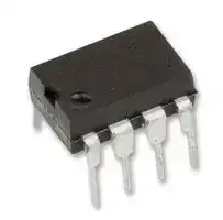
LCC120
MOSFET Relay, 250 V, 170 mA, 20 ohm, SPDT
⚠️ Reference pricing provided. In case of supply shortages, we will connect you with our trusted procurement partners to ensure your project's continuity.
- Manufacturer: CLARE
- Product type: MOSFET Solid State Relays
- Contact Configuration:SPDT; Load Current:170mA; Relay Terminals:Through Hole; Load Voltage Max:250V; On State Resistance Max:20ohm; Isolation Voltage:3.75kV; Forward Current If:10mA; Produc
- Load Type: AC / DC
- Contact Form: SPDT (1 Form C)
- Load Current: 170mA
- Product Range: OptoMOS Series
- Relay Mounting: Through Hole
- Relay Terminals: PC Pin
- Load Voltage Max: 250V
- Isolation Voltage: 3.75kV
- Forward Current If: 10mA
- I/O Capacitance Typ: 3pF
- Contact Configuration: SPDT
- On State Resistance Max: 20ohm
- MOSFET Relay Package Style: DIP-8
- Off State Leakage Current Max: 1µA
| Delivery and price | |
|---|---|
| Units per pack | 50 |
| Price | 3.64 € |
| Current stock | 10+ |
| Lead time | 30 days |
Datasheet

**LCC120 1-Form-C OptoMOS[®] Relay**
INTEGRATED CIRCUITS DIVISION
**Parameters Ratings Units** Blocking Voltage 250 VP Load Current 170 mArms / mADC On-Resistance (max) 20 ~~——~~
## **Features**
- 3750Vrms Input/Output Isolation
- 1-Form-C Solid State Relay
- Low Drive Power Requirements (TTL/CMOS Compatible)
- High Reliability
- Arc-Free With No Snubbing Circuits
- FCC Compatible
- VDE Compatible
- No EMI/RFI Generation
## **Description**
LCC120P is a 250V, 170mA, 20 1-Form-C relay. It is ideal for applications focused on peak load current handling capablilities.
This device is perfect for applications where a signal needs to be switched between two different lines. The small 8-lead package makes it an ideal space-saving replacement for a 1-Form-C electromechanical relay (EMR).
## **Approvals**
- UL Recognized Component: File E76270
- CSA Certified Component: Certificate # 1175739
- EN/IEC 60950-1 Certified Component:
- TUV Certificate B 09 07 49410 004
- Small 8-pin Package
- Machine Insertable, Wave Solderable
- Surface Mount Tape & Reel Versions Available
## **Applications**
- Telecommunications
- Telecom Switching
## **Ordering Information**
**Part # Description** LCC120 8-Pin DIP (50/Tube) LCC120S 8-Pin Surface Mount (50/Tube) LCC120STR 8-Pin Surfact Mount Tape & Reel (1000/Reel) ~~—_~~
- Tip/Ring Circuits
- Modem Switching (Laptop, Notebook, Pocket Size)
- Hook Switch
- Dial Pulsing
- Ground Start
- Ringing Injection
- Instrumentation
- Multiplexers
- Data Acquisition
- Electronic Switching
## **Pin Configuration**
**==> picture [201 x 82] intentionally omitted <==**
**----- Start of picture text -----**<br>
AC/DC Configuration<br>1 8<br>Do Not Use<br>Normally Closed Pole<br>2 7<br>+ Control<br>3 6<br>– Control<br>Normally Open Pole<br>4 5<br>Do Not Use<br>**----- End of picture text -----**<br>
- I/O Subsystems
- Meters (Watt-Hour, Water, Gas)
- Medical Equipment—Patient/Equipment Isolation
- Security
- Aerospace
## **Switching Characteristics for a Form-C Device**
- Industrial Controls
**==> picture [126 x 75] intentionally omitted <==**
**----- Start of picture text -----**<br>
IF<br>90%<br>Form-A ILOAD 10%<br>t on t off<br>Form-B ILOAD 90%<br>10%<br>t off t on<br>**----- End of picture text -----**<br>
> Pb e3 ~~oe~~ DS-LCC120-R09
**1**
**www.ixysic.com**
**LCC120**
INTEGRATED CIRCUITS DIVISION
## **Absolute Maximum Ratings @ 25ºC**
|**Parameter**|**Min**|**Max**|**Unit**|
|---|---|---|---|
|Blocking Voltage|-|250|VP|
|Reverse Input Voltage|-|5|V|
|Input control Current<br>Peak (10ms)|-<br>-|50|mA|
|||1|A|
|Input Power Dissipation1|-|150|mW|
|Total Power Dissipation2|-|800|mW|
|Isolation Voltage, Input to Output|3750|-|Vrms|
|Operating Temperature|-40|+85|ºC|
|Storage Temperature|-40|+125|ºC|
_Absolute Maximum Ratings are stress ratings. Stresses in excess of these ratings can cause permanent damage to the device. Functional operation of the device at conditions beyond those indicated in the operational sections of this data sheet is not implied._
1 Derate linearly 1.33mW / ºC.
2 Derate linearly 6.67mW / ºC.
## **Electrical Characteristics @ 25ºC**
|**Parameter**|**Conditions**|**Symbol**|**Min**|**Typ**|**Max**|**Units**|
|---|---|---|---|---|---|---|
|**Output Characteristics**<br>~~er~~|||||||
|Load Current<br>Continuous, AC/DC Confi guration<br>Peak<br>~~er~~|-<br>~~er~~|IL<br>~~er~~|-<br>~~er~~|-<br>~~er~~|170<br>~~er~~|mArms/ mADC<br>~~er~~|
||t=10ms<br>~~er~~|ILPK<br>~~er~~|-<br>~~er~~|-<br>~~er~~|±400<br>~~er~~|mAP<br>~~er~~|
|On-Resistance, AC/DC Confi guration<br>~~er~~|IL=170mA<br>~~er~~|RON<br>~~er~~|-<br>~~er~~|16<br>~~er~~|20<br>~~er~~|<br>~~er~~|
|Off-State Leakage Current<br>~~pT~~|VL=250VP<br>~~pT~~|ILEAK<br>~~pT~~|-<br>~~pT~~|-<br>~~pT~~|1<br>~~pT~~|µA<br>~~pT~~|
|Switching Speeds<br>Turn-On<br>Turn-Off<br>~~pT~~|IF=10mA, VL=10V<br>~~pT~~|ton<br>~~pT~~|-<br>~~pT~~|-<br>~~pT~~|5<br>~~pT~~|ms<br>~~pT~~|
|||toff<br>~~pT~~|-<br>~~pT~~|-<br>~~pT~~|5<br>~~pT~~||
|Output Capacitance|VL=50V, f=1MHz|COUT|-|50|-|pF|
|**Input Characteristics**|||||||
|Input Control Current to Activate|IL=170mA|IF|-|-|10|mA|
|Input Control Current to Deactivate|-|IF|0.4|0.7|-|mA|
|Input Voltage Drop|IF=10mA|VF|0.9|1.2|1.4|V|
|Reverse Input Current|VR=5V|IR|-|-|10|A|
|**Common Characteristics**|||||||
|Capacitance, Input to Output|-|CI/O|-|3|-|pF|
R09
**www.ixysic.com**
**2**
call INTEGRATED CIRCUITS DIVISION **LCC120** ~~a~~
## **COMMON PERFORMANCE DATA @25ºC (Unless Otherwise Noted)***
**==> picture [486 x 276] intentionally omitted <==**
**----- Start of picture text -----**<br>
Typical LED Forward Voltage Drop Typical LED Forward Voltage Drop Typical Leakage vs. Temperature<br>35 (N=50, IF=5mA) 1.8 vs. Temperature 0.016 Measured across Pins 5&6 or 7&8<br>30 0.014<br>1.6 PT TT Ee<br>0.012<br>25<br>20 1.4 SSECT [LLL)] E)|6URR [.] 0.010 hESee esto<br>0.008<br>15 1.2 SSS) 0.006 ee<br>10 0.004<br>1.0<br>5 0.002<br>0 0.8 SSFLL. 0 Seea<br>1.17 1.19 1.21 1.23 1.25 -40 -20 0 20 40 60 80 100 120 -40 -20 0 20 40 60 80 100<br>LED Forward Voltage Drop (V) Temperature (ºC) Temperature (ºC)<br>Energy Rating Curve<br>1.2<br>1.0<br>A TT TT<br>0.8 UN<br>0.6 A Tl<br>AINE ea A a<br>0.4<br>SCS<br>0.2 Oa AN ANY a eT<br>0 TITATIVE UI CTT<br>10 s 100 s 1ms 10ms 100ms 1s 10s 100s<br>Time<br>IIIIIFFFFF=50mA=30mA=20mA=10mA=5mA<br>A)<br>Leakage (<br>Device Count (N)<br>LED Forward Voltage Drop (V)<br>Load Current (A)<br>**----- End of picture text -----**<br>
## **FORM-A RELAY PERFORMANCE DATA @25ºC (Unless Otherwise Noted)***
**==> picture [482 x 286] intentionally omitted <==**
**----- Start of picture text -----**<br>
Form-A Form-A Form-A<br>Typical Turn-On Time Typical Turn-Off Time Typical On-Resistance Distribution<br>(N=50, IF=10mA, IL=170mADC) (N=50, IF=10mA, IL=170mADC) (N=50, IF=10mA, IL=170mADC)<br>25 25 35<br>30<br>20 20 ptt<br>25<br>15 15 Pt te)EP 20 e Re e<br>10 10 Se| See 15<br>10<br>5 5<br>miil 5 4 | =<br>0 0 | En | 0 HE<br>0.75 1.05 1.35 1.65 1.95 2.25 0.23 0.32 0.41 0.50 0.59 0.68 8.5 8.8 9.1 9.4 9.7 10.0 10.3<br>Turn-On Time (ms) Turn-Off Time (ms) On-Resistance ( )<br>Form-A Form-A Form-A<br>25 Typical I(N=50, IF for Switch OperationL=170mADC) 25 Typical I(N=50, IF for Switch DropoutL=170mADC) 35 Typical Blocking Voltage Distribution(N=50)<br>30<br>20 20<br>|| | get ll 25 ff fe ft ye<br>15 | |ii | 15 20 FCLCELeLe<br>10 ae | ee 10 15 ee<br>10<br>5 5<br>| [|] | 5 aB| a a<br>0 | | |) lh 0 0 | eae<br>1.05 1.75 2.45 3.15 3.85 4.55 5.25 1.05 1.75 2.45 3.15 3.85 4.55 5.25 330 340 350 360 370 380 390<br>LED Current (mA) LED Current (mA) Blocking Voltage (VP)<br>Device Count (N) Device Count (N) Device Count (N)<br>Device Count (N) Device Count (N) Device Count (N)<br>**----- End of picture text -----**<br>
*The Performance data shown in the graphs above is typical of device performance. For guaranteed parameters not indicated in the written specifications, please contact our application department.
R09
**www.ixysic.com**
**3**
eT INTEGRATED CIRCUITS DIVISION **LCC120** ~~ee~~
## **FORM-A RELAY PERFORMANCE DATA @25ºC (Unless Otherwise Noted)***
**==> picture [490 x 595] intentionally omitted <==**
**----- Start of picture text -----**<br>
Form-A Form-A Form-A<br>Typical Turn-On Time Typical IF for Switch Operation Typical Turn-On Time<br>vs. LED Forward Current vs. Temperature vs. Temperature<br>1.0 (IL=170mADC) 6 (IL=170mADC) 1.2 (IL=170mADC)<br>0.9 a IF=10mA<br>5 1.0 IF=15mA<br>0.8 IF=20mA<br>ESE 4 EEE) 0.8 Le<br>0.7<br>a LY St<br>0.60.50.40.3 eePERTSePOACPe e e 321 |eT[ir| [||] || || 0.60.40.2 FTpits]Ff]NET——PEest[tl<br>0.2 0 2 5 10 15 20 25 30 35 40 45 50 0-40 Ft -20 tt 0 20 40 tt 60 tt 80 100 0-40 PT -20 [tt}] 0 20 40 tT 60 tf 80 100<br>LED Forward Current (mA) Temperature (ºC) Temperature (ºC)<br>Form-A Form-A Form-A<br>Typical Turn-Off Time Typical IF for Switch Dropout Typical Turn-Off Time<br>vs. LED Forward Current vs. Temperature vs. Temperature<br>(IL=170mADC) (IL=170mADC) (IF=10mA, IL=170mADC)<br>0.25 6 0.8<br>0.7<br>0.20 PTT Z 5 ee<br>0.6<br>TEE tT 4 | ee<br>0.15 0.5<br>SH 3 eee 0.4 ESSE<br>0.10 0.3<br>SP 2 ee eS<br>0.2<br>0.05<br>FU) 1 ey 0.1 ERPS<br>0 PPE TTT [TTT)] 0 =~ 0 eee<br>0 5 10 15 20 25 30 35 40 45 50 -40 -20 0 20 40 60 80 100 -40 -20 0 20 40 60 80 100<br>LED Forward Current (mA) Temperature (ºC) Temperature (ºC)<br>Form-A<br>Typical On-Resistance Form-A Form-A<br>vs. Temperature Typical Load Current vs. Load Voltage Maximum Load Current<br>12 (IF=10mA, IL=170mADC) 150 (IF=10mA) 250 vs. Temperature<br>10 | | | | [ter 100 200 SS<br>¢ | EE<br>8 [| [[+]] 50<br>150<br>6 a | | 0 SSS<br>100<br>4 || |||| -50 SSS<br>2 a -100 50 itt<br>0 Ft | tt | tt -150 0 PE [TTT] tT TT Tt<br>-40 -20 0 20 40 60 80 100 -3 -2 -1 0 1 2 3 -40 -20 0 20 40 60 80 100 120<br>Temperature (ºC) Load Voltage (V) Temperature (ºC)<br>Form-A<br>Typical Blocking Voltage<br>vs. Temperature<br>350<br>345 [ | | [ [ [Fr |<br>340 | | | [| [[er]]<br>335 | |<br>330 | | | [er | | |<br>325 | |[er[er| {|[| | | |<br>320 Lat | {| {| | | |<br>315 rc | | [| [| | |<br>310 | | | [| [| [| | |<br>305 | [| [| [| [| [| J |<br>-40 -20 0 20 40 60 80 100<br>Temperature (ºC)<br>IIIFFF=30mA=20mA=10mA<br>Turn-On Time (ms) LED Current (mA) Turn-On Time (ms)<br>Turn-Off Time (ms) LED Current (mA) Turn-Off Time (ms)<br>On-Resistance () Load Current (mA) Load Current (mA)<br>)P<br>Blocking Voltage (V<br>**----- End of picture text -----**<br>
*The Performance data shown in the graphs above is typical of device performance. For guaranteed parameters not indicated in the written specifications, please contact our application department.
R09
**www.ixysic.com**
**4**
cal INTEGRATED CIRCUITS DIVISION **LCC120** ~~a~~
## **FORM-B RELAY PERFORMANCE DATA @25ºC (Unless Otherwise Noted)***
**==> picture [490 x 586] intentionally omitted <==**
**----- Start of picture text -----**<br>
Form-B Form-B Form-B<br>Typical Turn-On Time Typical Turn-Off Time Typical On-Resistance Distribution<br>(N=50, IF=10mA, IL=170mADC) (N=50, IF=10mA, IL=170mADC) (N=50, IF=10mA, IL=170mADC)<br>30 30 30<br>25 ee 25 25 (TL LELLL,<br>20151050 ee|| madd!) mi|| eelh 20151050 20151050 PELEatoeBaeeae|a|<br>0.25 0.35 0.45 0.55 0.65 0.75 0.6 1.0 1.4 1.8 2.2 2.6 9.3 10.2 11.1 12.0 12.9 13.8 14.7<br>Turn-On Time (ms) Turn-Off Time (ms) On-Resistance ( )<br>Form-B Form-B Form-B<br>Typical IF for Switch Operation Typical IF for Switch Dropout Typical Blocking Voltage Distribution<br>(N=50, IL=170mADC) (N=50, IL=170mADC) (N=50)<br>3025 se 2520 3025 TLTLELLLE,<br>20 se 20 rT [Ieee]<br>15 ae a 15 15 a. Se<br>10<br>10 | me 10 | =<br>50 aiia| = 50 50 aaaBaa<br>1.2 2.0 2.8 3.6 4.4 5.2 6.0 1.05 1.75 2.45 3.15 3.85 4.55 5.25 263 280 297 314 331 348 365<br>LED Current (mA) LED Current (mA) Blocking Voltage (VP)<br>Form-B Form-B Form-B<br>Typical Turn-On Time Typical IF for Switch Operation Typical Turn-On Time<br>vs.LED Forward Current vs. Temperature vs. Temperature<br>0.45 (IL=170mADC) 6 (IL=170mADC) 0.40 (IF=10mA, IL=170mADC)<br>0.35<br>0.40 SpbRePrTT yy) h 5 OF FEEre 0.30 NE<br>4<br>0.35 Creo 0.25 HH<br>3 0.20<br>0.30 POCO EERE 0.15 BREEREE<br>2<br>0.10<br>0.25 1<br>FILLET ETL) = feee erp 0.05 CSERS<br>0.20 PIL EL LEE 0 ©=©=6—E 0 FERTETFJ<br>0 5 10 15 20 25 30 35 40 45 50 -40 -20 0 20 40 60 80 100 -40 -20 0 20 40 60 80 100<br>LED Forward Current (mA) Temperature (ºC) Temperature (ºC)<br>Form-B Form-B Form-B<br>Typical Turn-Off Time Typical IF for Switch Dropout Typical Turn-Off Time<br>vs. LED Forward Current vs. Temperature vs. Temperature<br>1.6 (IL=170mADC) 6 (IL=170mADC) 2.5 (IL=170mADC)<br>1.4 TTT.LLELTLE (GC 5 CDC 2.0 IIFF=10mA=15mA /<br>1.2 FEELLEFEL 4 IF=20mA<br>I (6 CO 1.5 Xt LY<br>1.0 3<br>POPP) er 1.0 Ree<br>0.8 2<br>0.6 PONEPECE)ne 1 eerce 0.5 SS<br>0.4 POO 0 PPP COC 0 EEE EL LE<br>0 5 10 15 20 25 30 35 40 45 50 -40 -20 0 20 40 60 80 100 -40 -20 0 20 40 60 80 100<br>LED Forward Current (mA) Temperature (ºC) Temperature (ºC)<br>Device Count (N) Device Count (N) Device Count (N)<br>Device Count (N) Device Count (N) Device Count (N)<br>Turn-On Time (ms) LED Current (mA) Turn-On Time (ms)<br>Turn-Off Time (ms) LED Current (mA) Turn-Off Time (ms)<br>**----- End of picture text -----**<br>
*The Performance data shown in the graphs above is typical of device performance. For guaranteed parameters not indicated in the written specifications, please contact our application department.
R09
**www.ixysic.com**
**5**
cal INTEGRATED CIRCUITS DIVISION **LCC120** ~~a~~
## **FORM-B RELAY PERFORMANCE DATA @25ºC (Unless Otherwise Noted)***
**==> picture [488 x 292] intentionally omitted <==**
**----- Start of picture text -----**<br>
Form-B Form B<br>Typical On-Resistance Form-B Maximum Load Current<br>vs. Temperature Typical Load Current vs. Load Voltage vs. Temperature<br>60 (IF=10mA, IL=170mADC) 150 (IF=10mA) 250 (IF=10mA)<br>50 TTEEELEL 6 100 6 EfF OOo) 200 6NCOooe<br>40 50<br>gO 2 150 Se<br>30 0<br>100<br>20 TLELEL) 6 -50 6—Cee ~<br>10 a ee -100 50 J<br>0 ee -150 0 PEE LEE LI<br>-40 -20 0 20 40 60 80 100 -4 -3 -2 -1 0 1 2 3 4 -40 -20 0 20 40 60 80 100 120<br>Temperature (ºC) Load Voltage (V) Temperature (ºC)<br>Form-B<br>Typical Blocking Voltage<br>vs. Temperature<br>320<br>310<br>300 Pt | |[er]<br>290 | | | |r i] | |<br>280 | | PET i [| | |<br>270 | tt | ft tl lt<br>260 | | | {| [| ff<br>250 | tf | | [| ft ff<br>240 Lr ft | | [| [| ff<br>-40 -20 0 20 40 60 80 100<br>Temperature (ºC)<br>On-Resistance () Load Current (mA) Load Current (mA)<br>)P<br>Blocking Voltage (V<br>**----- End of picture text -----**<br>
*The Performance data shown in the graphs above is typical of device performance. For guaranteed parameters not indicated in the written specifications, please contact our application department.
R09
**www.ixysic.com**
**6**
**LCC120**
INTEGRATED CIRCUITS DIVISION
## **Manufacturing Information**
## **Moisture Sensitivity**
All plastic encapsulated semiconductor packages are susceptible to moisture ingression. IXYS Integrated Circuits Division classified all of its plastic encapsulated devices for moisture sensitivity according to ¢) the latest version of the joint industry standard, **IPC/JEDEC J-STD-020** , in force at the time of product evaluation. We test all of our products to the maximum conditions set forth in the standard, and guarantee proper operation of our devices when handled according to the limitations and information in that standard as well as to any limitations set forth in the information or standards referenced below.
Failure to adhere to the warnings or limitations as established by the listed specifications could result in reduced product performance, reduction of operable life, and/or reduction of overall reliability.
This product carries a **Moisture Sensitivity Level (MSL) rating** as shown below, and should be handled according to the requirements of the latest version of the joint industry standard **IPC/JEDEC J-STD-033** .
|**Device**<br>~~EE~~|**Moisture Sensitivity Level (MSL) Rating**<br>~~EE~~|
|---|---|
|LCC120 / LCC120S<br>~~EE~~|MSL 1<br>~~EE~~|
## **ESD Sensitivity**
This product is **ESD Sensitive** , and should be handled according to the industry standard **JESD-625** .
## **Reflow Profile**
This product has a maximum body temperature and time rating as shown below. All other guidelines of **J-STD-020** must be observed.
|**Device**<br>~~———~~|**Maximum Temperature x Time**<br>~~———~~|
|---|---|
|LCC120 / LCC120S<br>~~———~~|250ºC for 30 seconds<br>~~———~~|
## **Board Wash**
IXYS Integrated Circuits Division recommends the use of no-clean flux formulations. However, board washing to remove flux residue is acceptable. Since IXYS Integrated Circuits Division employs the use of silicone coating as an optical waveguide in many of its optically isolated products, the use of a short drying bake could be necessary if a wash is used after solder reflow processes. Chlorine- or Fluorine-based solvents or fluxes should not be used. Cleaning methods that employ ultrasonic energy should not be used.
## Pb e3 © ors
R09
**www.ixysic.com**
**7**
**LCC120**
INTEGRATED CIRCUITS DIVISION
## **Mechanical Dimensions**
## **LCC120**
**==> picture [429 x 515] intentionally omitted <==**
**----- Start of picture text -----**<br>
9.652 ± 0.381 7.620 ± 0.254 PCB Hole Pattern<br>2.540 ± 0.127 (0.380 ± 0.015) (0.300 ± 0.010)<br>(0.100 ± 0.005) 8-0.800 DIA. 2.540 ± 0.127<br>(8-0.031 DIA.) (0.100 ± 0.005)<br>9.144 ± 0.508<br>6.350 ± 0.127 (0.360 ± 0.020)<br>(0.250 ± 0.005)<br>6.350 ± 0.127<br>(0.250 ± 0.005)<br>Pin 1 3.302 ± 0.051<br>0.457 ± 0.076 (0.130 ± 0.002)<br>(0.018 ± 0.003) 7.239 TYP. 7.620 ± 0.127<br>(0.285) (0.300 ± 0.005)<br>7.620 ± 0.127<br>wR 4.064 TYP(0.160) , 0.254 ± 0.0127 toy (0.300 ± 0.005)<br>(0.010 ± 0.0005)<br>Dimensions<br>0.813 ± 0.102 mm<br>mr (0.032 ± 0.004) - (inches)<br>LCC120S<br>9.652 ± 0.381 PCB Land Pattern<br>(0.380 ± 0.015) 0.635 ± 0.127<br>2.540 ± 0.127 3.302 ± 0.051 (0.025 ± 0.005) 2.54<br>(0.100 ± 0.005) (0.130 ± 0.002) (0.10)<br>hod = o th<br>6.350 ± 0.127 9.525 ± 0.254<br>(0.250 ± 0.005) (0.375 ± 0.010) 1.65 8.90<br>7.620 ± 0.254 (0.0649) (0.3503)<br>Pin 1 (0.300 ± 0.010)<br>0.457 ± 0.076 0.254 ± 0.0127<br>(0.018 ± 0.003) (0.010 ± 0.0005) 0.65<br>(0.0255)<br>4.445 ± 0.127<br>(0.175 ± 0.005)<br>Dimensions<br>0.813 ± 0.102 mm<br>re (0.032 ± 0.004) - (inches)<br>LCC120STR Tape & Reel<br>330.2 DIA.<br>(13.00 DIA.)<br>Top Cover W=16.00<br>Tape Thickness Bo=10.30 (0.63)<br>0.102 MAX. (0.406)<br>(0.004 MAX.)<br>Ao=10.30 P=12.00<br>K0 =4.90 (0.406) (0.472)<br>(0.193)<br>K1 =4.20 User Direction of Feed<br>Embossed Carrier (0.165) Dimensions<br>mm<br>onee NOTES: (inches)<br>1. Dimensions carry tolerances of EIA Standard 481-2<br>Embossment 2. Tape complies with all “Notes” for constant dimensions listed on page 5 of EIA-481-2<br>For additional information please visit our website at: www.ixysic.com<br>**----- End of picture text -----**<br>
IXYS Integrated Circuits Division makes no representations or warranties with respect to the accuracy or completeness of the contents of this publication and reserves the right to make changes to specifications and product descriptions at any time without notice. Neither circuit patent licenses nor indemnity are expressed or implied. Except as set forth in IXYS Integrated Circuits Division’s Standard Terms and Conditions of Sale, IXYS Integrated Circuits Division assumes no liability whatsoever, and disclaims any express or implied warranty, relating to its products including, but not limited to, the implied warranty of merchantability, fitness for a particular purpose, or infringement of any intellectual property right.
The products described in this document are not designed, intended, authorized or warranted for use as components in systems intended for surgical implant into the body, or in other applications intended to support or sustain life, or where malfunction of IXYS Integrated Circuits Division’s product may result in direct physical harm, injury, or death to a person or severe property or environmental damage. IXYS Integrated Circuits Division reserves the right to discontinue or make changes to its products at any time without notice.
Specification: DS-LCC120-R09 ©Copyright 2012, IXYS Integrated Circuits Division OptoMOS[®] is a registered trademark of IXYS Integrated Circuits Division All rights reserved. Printed in USA.
**8**
12/22/2012
Updated at April 15, 2026
About Novapart
Novapart is a B2B electronic component broker specialising in stock shortages and cost reduction. We source hard-to-find parts and identify compliant alternatives across a catalogue of 410,000+ components from 500+ manufacturers.
Learn more →Stock Shortage Specialist
When a component is unavailable, discontinued or has an unacceptable lead time, we tap into our network of vetted European and Asian distributors to source what you need — without compromising on quality or traceability.
Request a quote →Compliant Alternatives
We identify pin-to-pin, electrically equivalent substitutes that meet the same certifications (RoHS, AEC-Q100, REACH) as your original specification — validated against datasheets, not just part numbers. Often at a lower cost.
BOM Analysis service →