
Image not available
Illustrative purposes only

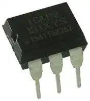
LCA110
MOSFET Relay, 350 V, 120 mA, 35 ohm, SPST-NO
⚠️ Reference pricing provided. In case of supply shortages, we will connect you with our trusted procurement partners to ensure your project's continuity.
- Manufacturer: CLARE
- Product type: MOSFET Solid State Relays
- Contact Configuration:SPST-NO; Load Current:120mA; Relay Terminals:Through Hole; Load Voltage Max:350V; On State Resistance Max:35ohm; Isolation Voltage:3.75kV; Forward Current If:2mA; Product Range:-; SVH
- Load Type: AC / DC
- Contact Form: SPST-NO (1 Form A)
- Load Current: 120mA
- Product Range: OptoMOS Series
- Relay Mounting: Through Hole
- Relay Terminals: PC Pin
- Load Voltage Max: 350V
- Isolation Voltage: 3.75kV
- Forward Current If: 2mA
- I/O Capacitance Typ: 3pF
- Contact Configuration: SPST-NO
- On State Resistance Max: 35ohm
- MOSFET Relay Package Style: DIP-6
- Off State Leakage Current Max: 1µA
| Delivery and price | |
|---|---|
| Units per pack | 100 |
| Price | 1.18 € |
| Current stock | 200+ |
| Lead time | 30 days |
Datasheet

**LCA110 Single Pole OptoMOS[®] Relays**

|**Parameter**|**Rating**|**Units**|
|---|---|---|
|Blocking Voltage|350|VP|
|Load Current|120|mA|
|Max On-resistance|35|Ω|


## **Features**

- 100% Solid State

- Small 6-Pin Package

- Low Drive Power Requirements (TTL/CMOS Compatible)

- High Reliability

- Arc-Free With No Snubbing Circuits

## **Description**

The LCA110 is a 1-Form-A Solid State Relay which uses optically coupled MOSFET technology to provide 3750Vrms of input to output isolation. The efficient MOSFET switches and photovoltaic die use Clare’s patented OptoMOS[®] architecture. The optically coupled output is controlled by a highly efficient GaAIAs infrared LED. The LCA110 can be used to replace mechanical relays and offers the superior reliability associated with semiconductor devices. Because they have no moving parts, they can offer faster, bounce-free switching in a more compact surface mount or though hole package.

- 3750Vrms Input/Output Isolation

- No EMI/RFI Generation

- Machine Insertable, Wave Solderable

- Surface Mount Tape & Reel Version Available

- Flammability classification rating of V-0

## **Approvals**

- UL Recognized: File Number E76270

- CSA Certified: File Number LR 43639-10

## **Applications**

   - EN/IEC 60950-1:2001 Compliant

- Instrumentation

- Multiplexers

- Data Acquisition

- Electronic Switching

- I/O Subsystems

- Meters (Watt-Hour, Water, Gas)

- Medical Equipment—Patient/Equipment Isolation

- Security

- Aerospace

- Industrial Controls

## **Ordering Information**

|**Part Number**|**Description**|
|---|---|
|LCA110|6-Pin DIP (50/Tube)|
|LCA110S|6-Pin Surface Mount (50/Tube)|
|LCA110STR|6-Pin Surface Mount (1,000/Reel)|


## **Pin Configuration**

**==> picture [235 x 49] intentionally omitted <==**

**----- Start of picture text -----**<br>
AC/DC Configuration DC Only Configuration<br>1 6 1 6<br>+ Control Load + Control + Load<br>2 5 2 5<br>– Control Do Not Use – Control – Load<br>3 4 3 4<br>N/C Load N/C<br>**----- End of picture text -----**<br>


## **Switching Characteristics of Normally Open (Form A) Devices**

**==> picture [80 x 50] intentionally omitted <==**

**----- Start of picture text -----**<br>
CONTROL<br>ILOAD 10%+ +90% 10%+<br>TON TOFF<br>**----- End of picture text -----**<br>


**==> picture [117 x 29] intentionally omitted <==**

**----- Start of picture text -----**<br>
RoHS<br>2002/95/EC<br>e3<br>&) OO<br>**----- End of picture text -----**<br>


DS-LCA110-R10

**1**

**www.clare.com**

**LCA110**

## **Absolute Maximum Ratings**

**==> picture [239 x 15] intentionally omitted <==**

**----- Start of picture text -----**<br>
Parameter Ratings Units<br>**----- End of picture text -----**<br>


|**Parameter**|**Ratings**|**Units**|
|---|---|---|
||||
|Blocking Voltage|350|VP|
|Reverse Input Voltage|5|V|
|Input Control Current<br>Peak (10ms)|50|mA|
||1|A|
|Input Power Dissipation1|150|mW|
|Total Power Dissipation2|800|mW|
|Isolation Voltage, Input to Output|3750|Vrms|
|Operational Temperature|-40 to +85|°C|
|Storage Temperature|-40 to +125|°C|


_Absolute Maximum Ratings are stress ratings. Stresses in excess of these ratings can cause permanent damage to the device. Functional operation of the device at conditions beyond those indicated in the operational sections of this data sheet is not implied._

1  Derate Linearly 1.33 mW/˚C

2  Derate Linearly 6.67 mW/˚C

Electrical absolute maximum ratings are at 25°C

## **Electrical Characteristics**

|**Parameter**|**Conditions**|**Symbol**|**Min**|**Typ**|**Max**|**Units**|
|---|---|---|---|---|---|---|
|**Output Characteristics @ 25°C**|||||||
|Load Current (Continuous)<br>AC/DC Configuration<br>DC Configuration|-|IL|-|-|120|mA|
||||-|-|200||
|Peak Load Current|t=10ms|ILPK|-|-|350|mA|
|On-resistance<br>AC/DC Configuration<br>DC Configuration|IL=120mA|RON|-|23|35|Ω|
||IL=200mA||-|7|10||
|Off-State Leakage Current|VL=350V|ILEAK|-|-|1|µA|
|Switching Speeds<br>Turn-On<br>Turn-Off|IF=5mA, VL=10V|TON|-|-|3|ms|
|||TOFF|||||
|Output Capacitance|50V; f=1MHz|COUT|-|25|-|pF|
|**Input Characteristics @ 25°C**|||||||
|Input Control Current|IL=120mA|IF|-|-|2|mA|
|Input Dropout Current|-|IF|0.4|-|-|mA|
|Input Voltage Drop|IF=5mA|VF|0.9|1.2|1.4|V|
|Reverse Input Current|VR=5V|IR|-|-|10|µA|
|**Common Characteristics @ 25°C**|||||||
|Input to Output Capacitance|-|CI/O|-|3|-|pF|


R10

**www.clare.com**

**2**

**LCA110**

## **PERFORMANCE DATA***

**==> picture [508 x 576] intentionally omitted <==**

**----- Start of picture text -----**<br>
LCA110 LCA110 LCA110<br>Typical LED Forward Voltage Drop Typical On-resistance Distribution Typical Blocking Voltage Distribution<br>(TA [ = 25°C; I] N=50F [ = 5mA] DC [)] (TA = 25°C; IN=50L = 120mADC) (TAN=50 = 25°C)<br>35 35 35<br>30 30 30<br>25 25 25<br>20 20 20<br>15 15 15<br>10 10 10<br>5 5 5<br>0 0 0<br>1.17 1.19 1.21 1.23 1.25 20.2 20.4 20.6 20.8 21.0 21.2 21.4 427 430 433 436 439 442<br>LED Forward Voltage Drop (V) On-resistance ( Ω ) Blocking Voltage (VP)<br>LCA110 LCA110 LCA110<br>Typical I(TA = 25°C; IF for Switch OperationN=50L = 120mADC) Typical I(TA = 25°C; IF for Switch DropoutN=50L = 120mADC) (TA = 25°C; ITypical Turn-On TimeL = 120mAN=50 DC; IF = 2mADC)<br>25 25 25<br>20 20 20<br>15 15 15<br>10 10 10<br>5 5 5<br>0 0 0<br>0.39 0.65 0.91 1.17 1.43 1.69 1.95 0.39 0.65 0.91 1.17 1.43 1.69 1.95 0.82 0.84 0.86 0.88 0.90 0.92 0.94<br>LED Current (mA) LED Current (mA) Turn-On (ms)<br>LCA110<br>Typical Turn-Off Time LCA110<br>(TA = 25°C; IL = 120mADC; IF = 2mADC) LCA110 Typical Leakage vs. Temperature<br>25 N=50 210 Typical Load Current vs. TemperatureDC Configuration 0.016 (Measured across Pins 4 & 6)<br>200<br>0.014<br>20 180<br>0.012<br>15 160140120 IIFF = 10mA = 5mA 0.0100.008<br>10 100 0.006<br>5 80 AC/DC Configuration IF = 10mA 0.004<br>60 IF = 5mA 0.002<br>0 0.285 0.295 0.305 0.315 0.325 0.335 0.345 0-40 -20 0 20 40 60 80 100 120 0-40 -20 0 20 40 60 80 100<br>Turn-Off (ms) Temperature (°C) Temperature (°C)<br>LCA110 LCA110 LCA110<br>Typical Blocking Voltage  Typical Turn-On vs. Temperature Typical Turn-Off vs. Temperature<br>430 vs. Temperature 5.0 (IL = 70mADC) 1.0 (IL = 70mADC; IF = 5mA)<br>425 4.5 0.9<br>4.0 0.8<br>420 3.5 0.7<br>415 3.0 0.6<br>2.5 0.5<br>410405 2.01.5 IF = 5mA 0.40.3<br>400 1.0 0.2<br>395 0.50 IF = 10mA 0.10<br>-40 -20 0 20 40 60 80 100 -40 -20 0 20 40 60 80 100 -40 -20 0 20 40 60 80 100<br>Temperature (°C) Temperature (°C) Temperature (°C)<br>Device Count (N) Device Count (N) Device Count (N)<br>Device Count (N) Device Count (N) Device Count (N)<br>Leakage (µA)<br>Device Count (N) Load Current (mA)<br>)P<br>Turn-On (ms) Turn-Off (ms)<br>Blocking Voltage (V<br>**----- End of picture text -----**<br>


*The Performance data shown in the graphs above is typical of device performance.  For guaranteed parameters not indicated in the written specifications, please contact our application department.

R10

**www.clare.com**

**3**

**LCA110**

## **PERFORMANCE DATA***

**==> picture [361 x 435] intentionally omitted <==**

**----- Start of picture text -----**<br>
LCA110 LCA110<br>Typical LED Forward Voltage Drop Typical Turn-On vs. LED Forward Current<br>1.8 vs. Temperature 2.0 (IL = 120mADC)<br>1.8<br>1.6 1.6<br>1.4<br>1.4 IF = 50mA 1.21.0<br>1.2 0.8<br>1.0 IIFF = 10mA = 5mA 0.60.4<br>0.2<br>0.8 0<br>-40 -20 0 20 40 60 80 100 120 0 5 10 15 20 25 30 35 40 45 50<br>Temperature (°C) LED Forward Current (mA)<br>LCA110 LCA110<br>On-resistance vs. TemperatureTypical Steady State  Typical Ivs. TemperatureF for Switch Operation<br>60 (IL = Max. rated @ temp.) 3.0 (IL = 70mADC)<br>50 2.5<br>40 IF=10mA 2.0<br>30 IF=5mA 1.5<br>20 1.0<br>10 0.5<br>0 0<br>-40 -20 0 20 40 60 80 100 -40 -20 0 20 40 60 80 100<br>Temperature (°C) Temperature (°C)<br>LCA110<br>Typical Load Current vs. Load Voltage<br>(TA = 25°C; IN=50F = 2mADC) Energy Rating CurveLCA110<br>150 1.0<br>0.9<br>100 0.8<br>0.7<br>50 0.6<br>0 0.5<br>0.4<br>-50 0.3<br>0.2<br>-100 0.1<br>-150 0<br>-3 -2 -1 0 1 2 3 10µs 100µs 1ms 10ms 100ms 1s 10s 100s<br>Load Voltage (V) Time<br>Turn-On (ms)<br>Turn-Off (ms)<br>LED Forward Voltage Drop (V)<br>) Ω<br>On-resistance ( LED Current (mA) LED Current (mA)<br>Load Current (mA) Load Current (A)<br>**----- End of picture text -----**<br>


**==> picture [144 x 125] intentionally omitted <==**

**----- Start of picture text -----**<br>
LCA110<br>Typical Turn-Off vs. LED Forward Current<br>(IL = 120mADC)<br>0.7<br>0.6<br>0.5<br>0.4<br>0.3<br>0.2<br>0.1<br>0<br>0 5 10 15 20 25 30 35 40 45 50<br>LED Forward Current (mA)<br>**----- End of picture text -----**<br>


**==> picture [139 x 131] intentionally omitted <==**

**----- Start of picture text -----**<br>
LCA110<br>Typical Ivs. TemperatureF for Switch Dropout<br>3.0 (IL = 70mADC)<br>2.5<br>2.0<br>1.5<br>1.0<br>0.5<br>0<br>-40 -20 0 20 40 60 80 100<br>Temperature (°C)<br>**----- End of picture text -----**<br>


*The Performance data shown in the graphs above is typical of device performance.  For guaranteed parameters not indicated in the written specifications, please contact our application department.

R10

**www.clare.com**

**4**

**LCA110**

## **Manufacturing Information**

## **Soldering**

For proper assembly, the component must be processed in accordance with the current revision of IPC/JEDEC standard J-STD-020. Failure to follow the recommended guidelines may cause permanent damage to the device resulting in impaired performance and/or a reduced lifetime expectancy.

## **Washing**

Clare does not recommend ultrasonic cleaning or the use of chlorinated solvents.

**==> picture [97 x 35] intentionally omitted <==**

**----- Start of picture text -----**<br>
RoHS<br>2002/95/EC<br>e3<br>**----- End of picture text -----**<br>


**==> picture [35 x 35] intentionally omitted <==**

Recommended soldering processes are limited to 260 º C component body temperature for 10 seconds.

## **MECHANICAL DIMENSIONS**

## **6-Pin DIP Through Hole (Standard)**

**==> picture [255 x 75] intentionally omitted <==**

**----- Start of picture text -----**<br>
7.620 ± 0.254 8.382 ± 0.381<br>(0.300 ± 0.010) (0.330 ± 0.015)<br>3.302 ± 0.051<br>(0.130 ± 0.002) 7.239 TYP 6.350 ± 0.127<br>(0.285 TYP) (0.250 ± 0.005)<br>0.254 TYP<br>(0.010 TYP) 9.144 ± 0.508 2.540 ± 0.127<br>(0.360 ± 0.020) (0.100 ± 0.005)<br>**----- End of picture text -----**<br>


**==> picture [141 x 97] intentionally omitted <==**

**----- Start of picture text -----**<br>
PC Board Pattern<br>(Top View)<br>2.540 ± 0.127<br>6-0.800 DIA. (0.100 ± 0.005)<br>(6-0.031 DIA.)<br>7.620 ± 0.127<br>6.350 ± 0.127 (0.300 ± 0.005)<br>(0.250 ± 0.005)<br>5.080 ± 0.127<br>(0.200 ± 0.005)<br>**----- End of picture text -----**<br>


## **6-Pin Surface Mount ("S" Suffix)**

**==> picture [460 x 110] intentionally omitted <==**

**----- Start of picture text -----**<br>
8.382 ± 0.381<br>7.620 ± 0.254 (0.330 ± 0.015) 2.540 ± 0.127 PC Board Pattern<br>(0.300 ± 0.010) (0.100 ± 0.005) (Top View) 2.540 ± 0.127<br>(0.100 ± 0.005)<br>3.302 ± 0.051 4.445 ± 0.127 9.525 ± 0.254<br>(0.130 ± 0.002) (0.175 ± 0.005) (0.375 ± 0.010)<br>6.350 ± 0.127<br>0.254 ± 0.0127 0.635 ± 0.127 (0.250 ± 0.005) 8.305 ± 0.127<br>(0.010 ± 0.0005) (0.025 ± 0.005) (0.327 ± 0.005)<br>1.905 ± 0.127<br>0.457 ± 0.076 (0.075 ± 0.005)<br>(0.018 ± 0.003)<br>1.499 ± 0.127<br>Tape and Reel Packaging for Surface Mount Package (0.059 ± 0.005)<br>**----- End of picture text -----**<br>


## **Tape and Reel Packaging for Surface Mount Package**

**==> picture [491 x 149] intentionally omitted <==**

**----- Start of picture text -----**<br>
330.2 DIA.<br>(13.00 DIA.)<br>Top Cover<br>Tape Thickness<br>0.102 MAX.<br>(0.004 MAX.) 1 6 W = 16.30 MAX(0.642 MAX)<br>B0 = 10.10<br>(0.398)<br>Top Cover<br>Tape<br>Embossment Carrier K0 = 4.90 P = 12.00 A0 = 10.10<br>       (0.193) (0.472) (0.398) Dimensions:<br>K1 = 3.80 mm<br>       (0.150) User Direction of Feed<br>Embossment (inches)<br>**----- End of picture text -----**<br>


R10

**www.clare.com**

**5**

**==> picture [507 x 35] intentionally omitted <==**

## **For additional information please visit our website at: www.clare.com**

_Clare, Inc. makes no representations or warranties with respect to the accuracy or completeness of the contents of this publication and reserves the right to make changes to specifications and product descriptions at any time without notice.  Neither circuit patent licenses nor indemnity are expressed or implied.  Except as set forth in Clare’s Standard Terms and Conditions of Sale, Clare, Inc. assumes no liability whatsoever, and disclaims any express or implied warranty, relating to its products including, but not limited to, the implied warranty of merchantability, fitness for a particular purpose, or infringement of any intellectual property right._

_The products described in this document are not designed, intended, authorized or warranted for use as components in systems intended for surgical implant into the body, or in other applications intended to support or sustain life, or where malfunction of Clare’s product may result in direct physical harm, injury, or death to a person or severe property or environmental damage.  Clare, Inc. reserves the right to discontinue or make changes to its products at any time without notice._

Specification:  DS-LCA110-R10 ©Copyright 2006, Clare, Inc. OptoMOS[®] is a registered trademark of Clare, Inc. All rights reserved.  Printed in USA. 10/23/06

**6**
Updated at April 15, 2026
About Novapart
Novapart is a B2B electronic component broker specialising in stock shortages and cost reduction. We source hard-to-find parts and identify compliant alternatives across a catalogue of 410,000+ components from 500+ manufacturers.
Learn more →Stock Shortage Specialist
When a component is unavailable, discontinued or has an unacceptable lead time, we tap into our network of vetted European and Asian distributors to source what you need — without compromising on quality or traceability.
Request a quote →Compliant Alternatives
We identify pin-to-pin, electrically equivalent substitutes that meet the same certifications (RoHS, AEC-Q100, REACH) as your original specification — validated against datasheets, not just part numbers. Often at a lower cost.
BOM Analysis service →