
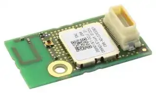


LBEE5ZZ1CK-982
Wireless LAN Module, 2.4 GHz, SDIO, UART, Aircraft, Aerospace, Undersea, Medical Equipment
- Manufacturer: MURATA
- Product type: WLAN Modules & USB Adaptors
- Frequency RF: 2.4GHz
- Module Interface: SDIO, UART
- Module Applications: Aircraft Equipment, Aerospace Equipment, Undersea Equipment, Medical Equipment
| Delivery and price | |
|---|---|
| Units per pack | 100 |
| Price | 11.98 € |
| Current stock | 10+ |
| Lead time | 30 days |
Preliminary Specification Number : SP-ZZ1CK-E

## **W-LAN+Bluetooth Combo Module Data Sheet**

## **Cypress Chipset for 802.11a/b/g/n/ac + Bluetooth 4.1**

## **- Tentative P/N : LBEE5ZZ1CK TEMP**

Preliminary < Specification may be changed by Murata without notice > Murata Manufacturing Co., Ltd.

Preliminary Specification Number : SP-ZZ1CK-E 1 / 32

## ~~SS~~ **The revision history of the product specification**

|RevisedNo.|Date|Note|
|---|---|---|
|-|2014/03/28|FirstIssue|
|B|2015/02/11|p4:Adding tolerance<br>p13~20:change output power|
|C|2016/4/14|P23:correctionoutput powersetting|
|D|2017/3/3|Changed IC Part Number<br>P3:Added Certification information<br>P5:Added Label information<br>P28:Added reference circuit<br>P29:AddedPackinginformation|
|E|2017/4/12|Revised BT version<br>P3:1. SCOPE<br>P27:11.10 DC/RF Characteristics for Bluetooth(LE)|


Preliminary < Specification may be changed by Murata without notice > Murata Manufacturing Co., Ltd.

Preliminary Specification Number : SP-ZZ1CK-E 2 / 32

## **TABLE OF CONTENTS**

|1.<br>SCOPE ....................................................................................................................................................... 3|
|---|
|2.<br>Part Number ............................................................................................................................................... 3|
|3.<br>Block Diaglam ............................................................................................................................................ 3|
|4.<br>Certification Information ............................................................................................................................. 3|
|4.1.<br>Radio Certification ..................................................................................................................... 3|
|5.<br>Dimensions,Marking and Terminal Configuration .................................................................................... 4|
|6.<br>Rating ......................................................................................................................................................... 8|
|7.<br>Operating Condition ................................................................................................................................... 8|
|7.1.<br>Operating condition .................................................................................................................... 8|
|7.2.<br>Power Up Sequence .................................................................................................................. 8|
|7.2.1<br>Power On Sequence for WLAN ON and BT ON ................................................................... 8|
|7.2.2<br>Power On Sequence for WLAN ON and BT Off .................................................................... 9|
|7.2.3<br>Power On Sequence for WLAN OFF and BT ON .................................................................. 9|
|7.2.4<br>Power On Sequence for WLAN OFF and BT OFF ................................................................ 9|
|8<br>External LPO Signal Requirement ........................................................................................................... 10|
|9.<br>Digital I/O Requirements .......................................................................................................................... 10|
|10<br>Interface timing ...................................................................................................................................... 11|
|10.1 WLAN SDIO Timing .................................................................................................................. 11|
|10.1.1<br>SDIO Timing(Default Mode) .................................................................................................. 11|
|10.1.2<br>SDIO Timing(High Speed Mode).......................................................................................... 12|
|10.1.3<br>SDIO timing(SDR mode) ...................................................................................................... 12|
|10.1.4<br>SDIO Timing(DDR50 mode) ................................................................................................ 15|
|10.2 Bluetooth UART Timing ........................................................................................................... 17|
|11 ELECTORICAL CHARACTERISTICS ..................................................................................................... 18|
|11.1<br>DC/RF Characteristics for IEEE802.11b - 2.4G ...................................................................... 18|
|11.2<br>DC/RF Characteristics for IEEE802.11g - 2.4G ...................................................................... 19|
|11.3<br>DC/RF Characteristics for IEEE802.11n - 2.4GHz .................................................................. 20|
|11.4<br>DC/RF Characteristics for IEEE802.11a - 5GHz ..................................................................... 21|
|11.5<br>DC/RF Characteristics for IEEE802.11n(HT 20MHz) - 5GHz ................................................. 22|
|11.6<br>DC/RF Characteristics for IEEE802.11n(HT 40MHz) - 5GHz ................................................. 23|
|11.7<br>DC/RF Characteristics for IEEE802.11ac(VHT 40MHz) - 5GHz ............................................. 24|
|11.8<br>DC/RF Characteristics for IEEE802.11ac(VHT 80MHz)-5GHz ............................................... 25|
|11.9<br>DC/RF Characteristics for Bluetooth ....................................................................................... 26|
|11.10<br>DC/RF Characteristics for Bluetooth(LE)........................................................................ 27|
|12<br>REFERENCE CIRCUIT........................................................................................................................ 28|
|13<br>Packing Information .............................................................................................................................. 29|
|NOTICE ........................................................................................................................................................... 31|
|1. Storage Conditions : .................................................................................................................................... 31|
|2. Handling Conditions :................................................................................................................................... 31|
|3. Cleaning : ..................................................................................................................................................... 31|
|4. Operational Environment Conditions : ......................................................................................................... 31|
|5. Input Power Capacity : ................................................................................................................................. 31|
|PRECONDITION TO USE OUR PRODUCTS ................................................................................................ 32|


Please be aware that an important notice concerning availability, standard warranty and use in critical applications of Murata products and disclaimers thereto appears at the end of this specification sheet.

Preliminary < Specification may be changed by Murata without notice > Murata Manufacturing Co., Ltd.

Preliminary Specification Number : SP-ZZ1CK-E 3 / 32

## **1. SCOPE**

This specification is applied to the IEEE802.11a/b/g/n/ac W-LAN + Bluetooth 4.1 combo module.

- Module size : 33.0 x 18.0 mm typ., t = 7.55 mm max. - IC/Firmware : Cypress CYW4339 - WLAN Host I/F : SDIO3.0 -Bluetooth Host I/F : UART - Reference Clock : 37.4MHz Crystal Oscillator embedded - ROM : Internal OTP - Weight : 2.47g - RoHS : This module is compliant with the RoHS directive.

## **2. Part Number**

Sample Part Number LBEE5ZZ1CK-TEMP

## **3. Block Diaglam**

## **4. Certification Information**

## **4.1. Radio Certification USA/Canada**

FCC ID : VPYLB1CK982 IC : 772C-LB1CK982

Preliminary < Specification may be changed by Murata without notice > Murata Manufacturing Co., Ltd.

Preliminary Specification Number : SP-ZZ1CK-E 4 / 32

## **5. Dimensions** , **Marking and Terminal Configuration**

## Dimensions

**==> picture [383 x 178] intentionally omitted <==**

**----- Start of picture text -----**<br>
33±0.2<br>23.7±0.2 9<br>4.3±0.2 2.7<br>30 1<br>φ2.7<br>±0.1<br>Shield Case<br>Internal<br>16 15 Antenna<br>3.1<br>±<br>9<br>0.2<br>±<br>0.2<br>18<br>±<br>0.2<br>**----- End of picture text -----**<br>


Unit:mm

Indication

< connector>

P/N: DF17(4.0)-30DP-0.5V (mounted on Murata module) P/N: DF17(4.0)-30DS-0.5V (need to place on Customer board) Maker: HIROSE Electric

## **Module**

**Module side connector [HIROSE] DF17(4.0)-30DP-0.5V Customer side connector [HIROSE] DF17(4.0)-30DS-0.5V**

## **Attachment**

**==> picture [114 x 12] intentionally omitted <==**

**----- Start of picture text -----**<br>
Customer Board<br>**----- End of picture text -----**<br>


Preliminary < Specification may be changed by Murata without notice > Murata Manufacturing Co., Ltd.

Preliminary Specification Number : SP-ZZ1CK-E 5 / 32

Marking <Top side>

**==> picture [150 x 96] intentionally omitted <==**

**----- Start of picture text -----**<br>
_LBEESZZ1CK-982 (A)<br>ID:VPYLBICK982 > (B)  oe<br>772C-LB1ICK982 (C)  es<br>982 2D Code<br>ABC  (D)<br>**----- End of picture text -----**<br>


|Marking||Meaning|
|---|---|---|
|(A)|Part Number||
|(B)|FCC ID||
|(C)|ICID||
|(D)|TraceNumber||


Preliminary < Specification may be changed by Murata without notice > Murata Manufacturing Co., Ltd.

Preliminary Specification Number : SP-ZZ1CK-E 6 / 32

Terminal Configurations

|No.|Terminal Name|Type|Connection to IC<br>Terminal|Description|
|---|---|---|---|---|
|1|VBAT|PI|SR_VDDBATP5V<br>LDO_VDDBAT5V|Power VBAT|
|2|VBAT|PI|SR_VDDBATP5V<br>LDO_VDDBAT5V|Power VBAT|
|3|GND|-|-|-|
|4|VIO|PI|PMU_VDDIO<br>VDDIO<br>VDDIO_SD|I/O supply for PMU, WLAN, SDIO|
|5|GND|-|-|-|
|6|WLAN_REG_ON|I|WL_REG_ON|Used by PMU to power up or power down<br>the internal CYW4339 regulators used by<br>the WLAN section. Also, when<br>deasserted, this pin holds the WLAN<br>section in reset. This pin has an internal<br>200k ohm pull-down resistor that is<br>enabled by default. It can be disabled<br>throughprogramming.|
|7|BT_REG_ON|I|BT_REG_ON|Used by PMU to power up, or power<br>down the internal CYW4339 regulators<br>used by BT section. Also when<br>deasserted, this pin holds the BT/FM<br>section in reset. This pin has an internal<br>200kohm pull-down resistor that is<br>enabled by default. It can be disabled by<br>programming.|
|8|WLAN_HOST_WAKE|I/O|GPIO_0|This pin can programmed by S/W to be a<br>GPIO, or WLAN_HOST_WAKE output<br>indicating that host wake-up should be<br>performed.|
|9|GND|-|-|-|
|10|BT_UART_RTS_N|O|BT_UART_RTS_N|UART request-to-send. Active-low<br>request to send signal for HCI UART I/F|
|11|BT_UART_TXD|O|BT_UART_TXD|UART signal output. Serial data output<br>fortheHCIUART I/F|
|12|BT_UART_RXD|I|BT_UART_RXD|UART signal input. Serial data input for<br>theHCIUART I/F|
|13|BT_UART_CTS_N|I|BT_UART_CTS_N|UART clear_ to_send.<br>Active low. Clear to send signal for HCI<br>UART I/F|
|14|GND|-|-|-|
|15|SLEEP_CLK|I|LPO_IN|ExternalSleep clock input(32.768kHz)|
|16|GND|-|-|-|
|17|BT_DEV_WAKE|I/O|BT_DEV_WAKE|DEV_WAKE of general purpose I/O<br>signal|
|18|BT_HOST_WAKE|I/O|BT_HOST_WAKE|HOST_WAKE of general purpose I/O<br>signal|
|19|GND|-|-||
|20|SDIO_D2|I/O|SDIO_DATA2|SDIO Data Line 2|
|21|GND|-|-|-|
|22|SDIO_D3|I/O|SDIO_DATA3|SDIO Data Line 3|
|23|GND|-|-|-|
|24|SDIO_CMD|I/O|SDIO_CMD|SDIO Command Line|
|25|GND|-|-|-|
|26|SDIO_CLK|I|SDIO_CLK|SDIO Clock Input|
|No.|Terminal Name|Type|Connection to IC<br>Terminal|Description|


Preliminary < Specification may be changed by Murata without notice > Murata Manufacturing Co., Ltd.

Preliminary Specification Number : SP-ZZ1CK-E 7 / 32

|27|GND|-|-|-|
|---|---|---|---|---|
|28|SDIO_D0|I/O|SDIO_DATA0|SDIO Data Line 0|
|29|GND|-|-|-|
|30|SDIO_D1|I/O|SDIO_DATA1|SDIO Data Line 1|


Terminal Configuration looked from a board implementation side of the customer

**==> picture [195 x 183] intentionally omitted <==**

**----- Start of picture text -----**<br>
(16)  (15)<br>(30)  (1)<br>**----- End of picture text -----**<br>


Preliminary < Specification may be changed by Murata without notice > Murata Manufacturing Co., Ltd.

Preliminary Specification Number : SP-ZZ1CK-E 8 / 32

## **6. Rating**

|Parameter|Parameter|min.|max.|Unit|
|---|---|---|---|---|
|StorageTemperature||-40|85|deg.C|
|Supply Voltage|VBAT|0|+5|V|
||VIO|0|+3.9|V|


- Stresses in excess of the absolute ratings may cause permanent damage. Functional operation is not implied under these conditions. Exposure to absolute ratings for extended periods of time may adversely affect reliability. No damage assuming only one parameter is set at limit at a time with all other parameters are set within operating condition.

## **7. Operating Condition**

|Parameter|Parameter|min.|typ.|max.|unit|
|---|---|---|---|---|---|
|OperatingTemperature*1||-20|25|80|deg.C|
|Supply Voltage|VBAT|3.2|3.6|4.4|V|
||VIO|1.71|1.8|1.89|V|


- Surface temperature of shield case

## **7.2. Power Up Sequence**

-VBAT should not rise 10%-90%faster than 40 microsecond.

-VBAT should be up before or at the same time as VIO. VIO should NOT be present fast or be held high before VBAT is high.

## **7.2.1 Power On Sequence for WLAN ON and BT ON**

**==> picture [428 x 156] intentionally omitted <==**

**----- Start of picture text -----**<br>
32.768kHz Sleep Clock<br>we<br>VBAT 90% of VH<br>i ce<br>VDDIOVIO<br>~2 Sleep cycle<br>WL_REG_ON<br>BT_REG_ON<br>**----- End of picture text -----**<br>


Preliminary < Specification may be changed by Murata without notice > Murata Manufacturing Co., Ltd.

Preliminary Specification Number : SP-ZZ1CK-E 9 / 32 muRata ~~oe~~

## **7.2.2 Power On Sequence for WLAN ON and BT OFF**

|32.768kHz Sleep Clock<br>VBAT<br>VDDIO<br>WL_REG_ON<br>VIO|90% of VH<br>~2 Sleep cycle<br>~~ITLILILILILI~~<br>~~LILILILI LI LIL~~<br>~~7~~<br>~~ce~~|90% of VH<br>~2 Sleep cycle<br>~~ITLILILILILI~~<br>~~LILILILI LI LIL~~<br>~~7~~<br>~~ce~~|90% of VH<br>~2 Sleep cycle<br>~~ITLILILILILI~~<br>~~LILILILI LI LIL~~<br>~~7~~<br>~~ce~~|90% of VH<br>~2 Sleep cycle<br>~~ITLILILILILI~~<br>~~LILILILI LI LIL~~<br>~~7~~<br>~~ce~~|90% of VH<br>~2 Sleep cycle<br>~~ITLILILILILI~~<br>~~LILILILI LI LIL~~<br>~~7~~<br>~~ce~~|90% of VH<br>~2 Sleep cycle<br>~~ITLILILILILI~~<br>~~LILILILI LI LIL~~<br>~~7~~<br>~~ce~~|90% of VH<br>~2 Sleep cycle<br>~~ITLILILILILI~~<br>~~LILILILI LI LIL~~<br>~~7~~<br>~~ce~~|90% of VH<br>~2 Sleep cycle<br>~~ITLILILILILI~~<br>~~LILILILI LI LIL~~<br>~~7~~<br>~~ce~~|90% of VH<br>~2 Sleep cycle<br>~~ITLILILILILI~~<br>~~LILILILI LI LIL~~<br>~~7~~<br>~~ce~~|90% of VH<br>~2 Sleep cycle<br>~~ITLILILILILI~~<br>~~LILILILI LI LIL~~<br>~~7~~<br>~~ce~~|90% of VH<br>~2 Sleep cycle<br>~~ITLILILILILI~~<br>~~LILILILI LI LIL~~<br>~~7~~<br>~~ce~~|90% of VH<br>~2 Sleep cycle<br>~~ITLILILILILI~~<br>~~LILILILI LI LIL~~<br>~~7~~<br>~~ce~~|90% of VH<br>~2 Sleep cycle<br>~~ITLILILILILI~~<br>~~LILILILI LI LIL~~<br>~~7~~<br>~~ce~~|90% of VH<br>~2 Sleep cycle<br>~~ITLILILILILI~~<br>~~LILILILI LI LIL~~<br>~~7~~<br>~~ce~~|90% of VH<br>~2 Sleep cycle<br>~~ITLILILILILI~~<br>~~LILILILI LI LIL~~<br>~~7~~<br>~~ce~~|90% of VH<br>~2 Sleep cycle<br>~~ITLILILILILI~~<br>~~LILILILI LI LIL~~<br>~~7~~<br>~~ce~~|
|---|---|---|---|---|---|---|---|---|---|---|---|---|---|---|---|---|
|BT_REG_ON|||||||||||||||||
||||||||||||||||||
|**7.2.3**<br>**Power On Sequence for WLAN OFF and BT ON**|||||||||||||||||
|32.768kHz Sleep Clock<br>VBAT<br>VDDIO<br>VIO|90% of VH<br>~2 Sleep cycle<br>~~JLILILILI~~<br>LLU LILI LI LI LU<br>~~ZZ~~<br>~~|~~=||||||||||||||||
|WL_REG_ON|||||||||||||||||
||||||||||||||||||
|BT_REG_ON|||||||||||||||||


## **7.2.3 Power On Sequence for WLAN OFF and BT ON**

|**7.2.4**<br>**Power On Sequence for WLAN OFF and BT OFF**|**7.2.4**<br>**Power On Sequence for WLAN OFF and BT OFF**|**7.2.4**<br>**Power On Sequence for WLAN OFF and BT OFF**|**7.2.4**<br>**Power On Sequence for WLAN OFF and BT OFF**|**7.2.4**<br>**Power On Sequence for WLAN OFF and BT OFF**|**7.2.4**<br>**Power On Sequence for WLAN OFF and BT OFF**|**7.2.4**<br>**Power On Sequence for WLAN OFF and BT OFF**|**7.2.4**<br>**Power On Sequence for WLAN OFF and BT OFF**|**7.2.4**<br>**Power On Sequence for WLAN OFF and BT OFF**|**7.2.4**<br>**Power On Sequence for WLAN OFF and BT OFF**|**7.2.4**<br>**Power On Sequence for WLAN OFF and BT OFF**|**Power On Sequence for WLAN OFF and BT OFF**|**Power On Sequence for WLAN OFF and BT OFF**|**Power On Sequence for WLAN OFF and BT OFF**|
|---|---|---|---|---|---|---|---|---|---|---|---|---|---|
||~~FLILILILILILI~~|~~FLILILILILILI~~|~~FLILILILILILI~~|~~FLILILILILILI~~|~~FLILILILILILI~~|~~FLILILILILILI~~|~~FLILILILILILI~~|~~FLILILILILILI~~|~~FLILILILILILI~~|~~FLILILILILILI~~|~~FLILILILILILI~~|~~FLILILILILILI~~|~~FLILILILILILI~~|
|32.768kHz Sleep Clock|~~FLILILILILILI~~|~~FLILILILILILI~~|~~FLILILILILILI~~|~~FLILILILILILI~~|~~FLILILILILILI~~|~~FLILILILILILI~~|~~FLILILILILILI~~|~~FLILILILILILI~~|~~FLILILILILILI~~|~~FLILILILILILI~~|~~FLILILILILILI~~|~~FLILILILILILI~~|~~FLILILILILILI~~|
|VBAT||||||||||||||
|VDDIO<br>VIO||||||||||||||
|WL_REG_ON||||||||||||||
|BT_REG_ON||||||||||||||


Preliminary < Specification may be changed by Murata without notice > Murata Manufacturing Co., Ltd.

Preliminary Specification Number : SP-ZZ1CK-E 10 / 32

## **8 External LPO Signal Requirement**

|Parameter|External LPO Clock|Unit|
|---|---|---|
|Nominal inputfrequency|32.768|kHz|
|Frequency accuracy|+/-200|ppm|
|Duty cycle|30-70|%|
|Input signal amplitude|200-1800|mVp-p|
|Signaltype|Square-wave orsine-wave|-|
|Input impedance*a|> 100k<br>< 5|ohm<br>pF|
|Clockjitter(duringinitialstart-up)|<10,000|ppm|


a)When power is applied or switch off.

## **9. Digital I/O Requirements**

|Digital I/O Pins|Sym|min.|typ.|max.|unit|
|---|---|---|---|---|---|
|SDIO Interface I/O Pins@1.8V||||||
|Input high voltage|VIH|1.27|-|-|V|
|Input low voltage|VIL|-|-|0.58|V|
|Output high voltage@2mA|VOH|1.40|-|-|V|
|Output low voltage@2mA|VOL|-|-|0.45|V|
|Other Digital I/O Pins@1.8V||||||
|Input high voltage|VIH|0.65 x VIO|-|-|V|
|Input low voltage|VIL|-|-|0.35 x VIO|V|
|Output high voltage@2mA|VOH|VIO-0.45|-|-|V|
|Output low voltage@2mA|VOL|-|-|0.45|V|


Preliminary < Specification may be changed by Murata without notice > Murata Manufacturing Co., Ltd.

Preliminary Specification Number : SP-ZZ1CK-E 11 / 32

## **10 Interface timing 10.1 WLAN SDIO Timing**

## **10.1.1 SDIO Timing(Default Mode)**

**==> picture [246 x 163] intentionally omitted <==**

**----- Start of picture text -----**<br>
fPP<br>ee al<br>tWL tWH<br>— > EE al<br>CLK<br>tTH L tTLH<br>-_ tISU tIH<br>+->_<br>Input<br>Output<br>—<——q- —_><br>tODLY tODLY<br>(max) (min)<br>**----- End of picture text -----**<br>


SDIO Bus Timing[(a)] parameters (default Mode)

**==> picture [435 x 173] intentionally omitted <==**

**----- Start of picture text -----**<br>
|||||||
|---|---|---|---|---|---|
|Parameter|Symbol|Min|Typ|Max|Unit|
|SDIO|CLK (All values|are referred|to minimum VIH and maximum VIL|[(b)]|
|Frequency-Data Transfer Mode|fPP|0|-|25|MHz|
|Frequency-Identification Mode|fOD|0|-|400|kHz|
|Clock Low Time|tWL|10|-|-|ns|
|Clock High Time|tWH|10|-|-|ns|
|Clock Rise Time|tTLH|-|-|10|ns|
|Clock low Time|tTHL|-|-|10|ns|
|Inputs: CMD, DAT (referenced|to|CLK)|
|Input Setup Time|tISU|5|-|-|ns|
|Input Hold Time|tIH|5|-|-|ns|
|Outputs: CMD, DAT (referenced|to|CLK)|
|Output Delay time-Data Transfer Mode|tODLY|0|-|14|ns|
|Output Delay time-Identification Mode|tODLY|0|-|50|ns|

**----- End of picture text -----**<br>


(a). Timing is based on CL < 40pF load on CMD and Data.

(b). Min (Vih) = 0.7*VIO and max (Vil) = 0.2*VIO.

Preliminary < Specification may be changed by Murata without notice > Murata Manufacturing Co., Ltd.

Preliminary Specification Number : SP-ZZ1CK-E 12 / 32

## **10.1.2 SDIO Timing(High Speed Mode)**

**==> picture [267 x 170] intentionally omitted <==**

**----- Start of picture text -----**<br>
fPP<br>al<br>50% VDD tWL tWH<br>SDIO_     CLK<br>FF\_ tTH L al tTLH eef<br>id tISU —_ tIH \<br>+> +<br>Input<br>Output<br>XX<br>tODLY tOH<br>SDIO Bus Timing [(a)] parameters (High-Speed Mode)<br>**----- End of picture text -----**<br>


|Parameter<br>~~ee~~<br>~~Cn~~|Symbol<br>~~ee~~<br>|Min<br>~~ee~~<br>|Typ<br>~~ee~~<br>|Max<br>~~ee~~<br>|Unit<br>~~ee~~<br>|
|---|---|---|---|---|---|
|SDIO CLK(All values arereferred tominimum VIHandmaximum VIL(b)<br>~~Cn~~||||||
|Frequency-Data Transfer Mode<br>~~CnQO~~<br>~~I~~|fPP<br>~~QO~~<br>|0<br>~~QO~~<br>|-<br>~~QO~~<br>|50<br>~~QO~~<br>|MHz<br>~~QO~~<br>|
|Frequency-Identification Mode<br>~~QO~~<br>~~I~~|fOD<br>~~QO~~<br>|0<br>~~QO~~<br>|-<br>~~QO~~<br>|400<br>~~QO~~<br>|kHz<br>~~QO~~<br>|
|Clock Low Time<br>~~IQO~~<br>~~I~~|tWL<br>~~QO~~<br>|7<br>~~QO~~<br>|-<br>~~QO~~<br>|-<br>~~QO~~<br>|ns<br>~~QO~~<br>|
|Clock High Time<br>~~QO~~<br>~~I~~|tWH<br>~~QO~~<br>|7<br>~~QO~~<br>|-<br>~~QO~~<br>|-<br>~~QO~~<br>|ns<br>~~QO~~<br>|
|Clock Rise Time<br>~~IGs~~|tTLH<br>~~Gs~~|-<br>~~Gs~~|-<br>~~Gs~~|3<br>~~Gs~~|ns<br>~~Gs~~|
|Clock low Time<br>~~QO~~|tTHL<br>~~QO~~|-<br>~~QO~~|-<br>~~QO~~|3<br>~~QO~~|ns<br>~~QO~~|
|Inputs:CMD,DAT(referenced to CLK)<br>~~QO~~<br>~~Ce~~||||||
|Input SetupTime<br>~~sO~~|tISU<br>~~sO~~|6<br>~~sO~~|-<br>~~sO~~|-<br>~~sO~~|ns<br>~~sO~~|
|Input Hold Time<br>~~sO~~<br>~~rs~~<br>~~Cn~~|tIH<br>~~sO~~<br>~~rs~~<br>|2<br>~~sO~~<br>~~rs~~<br>|-<br>~~sO~~<br>~~rs~~<br>|-<br>~~sO~~<br>~~rs~~<br>|ns<br>~~sO~~<br>~~rs~~<br>|
|Outputs: CMD, DAT (referenced to CLK)<br>~~Cn~~||||||
|Output Delaytime-Data Transfer Mode<br>~~CnQO~~|tODLY<br>~~QO~~|-<br>~~QO~~|-<br>~~QO~~|14<br>~~QO~~|ns<br>~~QO~~|
|Output Hold time<br>~~rr~~|tOH<br>~~rr~~|2.5<br>~~rr~~|-<br>~~rr~~|-<br>~~rr~~|ns<br>~~rr~~|
|Total System Capacitance(each line)<br>~~QO~~|CL<br>~~QO~~|-<br>~~QO~~|-<br>~~QO~~|40<br>~~QO~~|pF<br>~~QO~~|


(a). Timing is based on CL < 40pF load on CMD and Data.

(b). Min (Vih) = 0.7*VIO and max (Vil) = 0.2*VIO.

## **10.1.3 SDIO timing(SDR mode)**

Clock Timing

## SDIO Bus Clock Timing Parameters(SDR Modes)

|Parameter|Symbol|Min|Max|Unit|Comments|
|---|---|---|---|---|---|
|-|tclk|40|-|ns|SDR12 mode|
|||20|-|ns|SDR25mode|
|||10|-|ns|SDR50mode|
|||4.8|-|ns|SDR104 mode|
|-|tcr, tcf|-|0.2xtclk|ns|tcr, tcf<2.00ns(max)@100MHz,<br>Ccard=10pF<br>tcr, tcf<0.96ns(max)@208MHz,<br>Ccard=10pF|
|Clock duty<br>cycle|-|30|70|%|ns|


Preliminary

< Specification may be changed by Murata without notice > Murata Manufacturing Co., Ltd.

Preliminary Specification Number : SP-ZZ1CK-E 13 / 32

Device Input Timing

## SDIO Bus Input Timing Parameters(SDR Modes)

|Symbol|Min|Max|Unit|CommentsUnit|
|---|---|---|---|---|
|**SDR104 Mode**|||||
|tis|1.4|-|ns|Ccard=10pF,VCT=0.975V|
|tih|0.8|-|ns|Ccard=5pF, VCT=0.975v|
|**SDR50 Mode**|||||
|tis|3.0|-|ns|Ccard=10pF,VCT=0.975V|
|tih|0.8|-|ns|Ccard=5pF,VCT=0.975V|


Device Output Timing

SDR Modes up to 100MHz

SDIO Bus Output Timing Parameters(SDR Modes up to 100MHz)

|Symbol|Min|Max|Unit|CommentsUnit|
|---|---|---|---|---|
|todly|-|7.5|ns|tclk>10ns Cl=30pFusing drivertyoeB forSDR50|
|todly|-|14.0|ns|tclk>20ns Cl=40pF using for SDR12, SDR25|
|toh|1.5|-|ns|Hold time at the todly(min) Cl=15pF|


Preliminary < Specification may be changed by Murata without notice > Murata Manufacturing Co., Ltd.

Preliminary Specification Number : SP-ZZ1CK-E 14 / 32

SDR Modes 100MHz to 208MHz

SDIO Bus Output Timing Parameters(SDR Modes 100MHz up to 208MHz)

|Symbol|Min|Max|Unit|Comments|
|---|---|---|---|---|
|top|0|2|UI|Card output phase|
|⊿top|-350|+1550|ps|Delayvariation due to tempchange after tuning|
|todw|0.60|-|UI|todw=2.88ns@208MHz|


⊿ top=+1550 ps for junction temperature of ⊿ top=90 degrees during operation

⊿ top=-350 ps for junction temperature of ⊿ top=-20 degrees during operation

- ⊿ top=+2600 ps for junction temperature of ⊿ top=-20 to +125 degrees during operation

⊿ top Consideration for Variable Data Window (SDR 104 mode)

Preliminary < Specification may be changed by Murata without notice > Murata Manufacturing Co., Ltd.

Preliminary Specification Number : SP-ZZ1CK-E 15 / 32

## **10.1.4 SDIO Timing(DDR50 mode)**

## SDIO Bus Clock Timing Parameters(DDR50 Mode)

|parameter|Symbol|Min|Max|Unit|Comments|
|---|---|---|---|---|---|
|-|tclk|20|-|ns|DDR50mode|
|-|tcr, tcf|-|0.2xtclk|ns|tcr, tcf<4.00ns(max)@50MHz,<br>Ccard=10pF|
|Clockduty cycle|-|45|55|%|-|


Preliminary < Specification may be changed by Murata without notice > Murata Manufacturing Co., Ltd.

Preliminary Specification Number : SP-ZZ1CK-E 16 / 32

Data Timing, DDR50 Mode

## SDIO Bus Timing Parameters(DDR50 Mode)

|parameter|Symbol|Min|Max|unit|Comments|
|---|---|---|---|---|---|
|**Input CMD**||||||
|Input setup time|tisu|6|-|ns|Ccard<10pF(1 Card)|
|Inputhold time|tih|0.8|-|ns|Ccard<10pF(1Card)|
|**Output CMD**||||||
|Output delay time|todly|-|13.7|ns|Ccard<30pF(1Card)|
|Output hold time|toh|1.5|-|ns|Ccard<15pF(1 Card)|
|**Input DAT**||||||
|Input setup time|tisu2x|3|-|ns|Ccard<10pF(1Card)|
|Inputhold time|tih2x|0.8|-|ns|Ccard<10pF(1Card)|
|**Output DAT**||||||
|Output delay time|todly2x|-|7.0|ns|Ccard<25pF(1Card)|
|Outputhold time|todly2x|1.5|-|ns|Ccard<15pF(1Card)|


Preliminary < Specification may be changed by Murata without notice > Murata Manufacturing Co., Ltd.

Preliminary Specification Number : SP-ZZ1CK-E 17 / 32

## **10.2 Bluetooth UART Timing**

**==> picture [494 x 114] intentionally omitted <==**

**----- Start of picture text -----**<br>
BT_UART_CTS_N I<br>I<br>DTT TT 2 ] Midpoint of STOP bit<br>es eS a —<br>BT_UART_TXD I| I<br>\<br>| 1 ey 2 Cy Ce<br>—— 1<br>a Midpoint of STOP bit<br>BT_UART_RXD I<br>_ ey, ] 3<br>k——>1<br>BT_UART_RTS_N ]<br>**----- End of picture text -----**<br>


|Reference|Description|Min|Typ|Max|Unit|
|---|---|---|---|---|---|
|1|Delaytime, UART_CTS low to UART_TXD valid|-|-|1.5|Bit periods|
|2|Setuptime, UART_CTS high before midpoint of stopbit|-|-|0.5|Bit periods|
|3|Delaytime, midpoint of stopbit to UART_RTS high|-|-|0.5|Bit periods|


Preliminary < Specification may be changed by Murata without notice > Murata Manufacturing Co., Ltd.

Preliminary Specification Number : SP-ZZ1CK-E 18 / 32

## **11 ELECTORICAL CHARACTERISTICS**

## **11.1 DC/RF Characteristics for IEEE802.11b - 2.4G**

Normal Condition : 25deg.C, VBAT=3.6V.

11Mbps mode unless otherwise specified.

|**Items**|**Contents**|**Contents**|**Contents**|**Contents**|
|---|---|---|---|---|
|Specification|IEEE802.11b-2.4GHz||||
|Mode|DSSS / CCK||||
|Channel frequency|2412to2472 MHz||||
|Datarate|1,2, 5.5,11Mbps||||
|Powersetting (Txpower,indBm)|17||||
|**Current Consumption **|**Min.**|**Typ. **|**Max.**|**unit**|
|(a)Tx mode (99%Tx mode)|-|-|350|mA|
|(b)Rx mode|-|-|100|mA|
|**Transmitter**|**Min.**|**Typ. **|**Max.**|**Unit**|
|Power Levels|15|17|19|dBm|
|Spectrum Mask|||||
|(a)1st sidelobes|-|-|-30|dBr|
|(b)2nd sidelobes|-|-|-50|dBr|
|Power-on/off ramp|-|-|2.0|Usec|
|RFCarrierSuppression|15||-|dB|
|Modulation Accuracy|-|-|35|%|
|Spurious Emissions(BW=100kHz)|||||
|(a)10MHz≦f<2387MHz|-|-|-36|dBm|
|(b)2387MHz≦f<2400MHz|-|-|-30|dBm|
|(c)2483.5MHz<f≦2496.5MHz|-|-|-47|dBm|
|(d)2496.5MHz<f≦8GHz|-|-|-47|dBm|
|**Receiver**|**Min.**|**Typ. **|**Max.**|**Unit**|
|Minimum InputLevel(FER< 8%)|-|-|-76|dBm|
|Maximum InputLevel(FER< 8%)|-10|-|-|dBm|
|Adjacent Channel Rejection(FER< 8%)|35|-|-|dB|


Preliminary < Specification may be changed by Murata without notice > Murata Manufacturing Co., Ltd.

Preliminary Specification Number : SP-ZZ1CK-E 19 / 32

## **11.2 DC/RF Characteristics for IEEE802.11g - 2.4G**

Normal Condition : 25deg.C, VBAT =3.6V.

54Mbps mode unless otherwise specified.

|**Items**|**Contents**|**Contents**|**Contents**|**Contents**|
|---|---|---|---|---|
|Specification|IEEE802.11g-2.4GHz||||
|Mode|OFDM||||
|Channel frequency|2412to2472 MHz||||
|Datarate|6, 9,12,18,24, 36,48, 54Mbps||||
|Powersetting (Txpower,indBm)|14||||
|**Current Consumption **|**Min.**|**Typ. **|**Max.**|**Unit**|
|(a) Tx mode (99% Tx mode)|-|-|300|mA|
|(b)Rx mode|-|-|100|mA|
|**Transmitter**|**Min.**|**Typ. **|**Max.**|**Unit**|
|Power Levels|12|14|16|dBm|
|Spectrum Mask|||||
|(a) atfc +/- 11MHz|-|-|-20|dBr|
|(b) atfc +/- 20MHz|-|-|-28|dBr|
|(c) atfc >+/-30MHz|-|-|-40|dBr|
|Constellation Error|-|-|-25|dB|
|Spurious Emissions(BW=100kHz)|||||
|(a)10MHz≦f<2387MHz|-|-|-36|dBm|
|(b)2387MHz≦f<2400MHz|-|-|-30|dBm|
|(c)2483.5MHz<f≦2496.5MHz|-|-|-47|dBm|
|(d)2496.5MHz<f≦8GHz|-|-|-47|dBm|
|**Receiver**|**Min.**|**Typ. **|**Max.**|**Unit**|
|Minimum InputLevel(PER<10%)|-|-|-65|dBm|
|Maximum InputLevel(PER<10%)|-20|-|-|dBm|
|Adjacent Channel Rejection(FER<10%)|-1|-|-|dB|


Preliminary < Specification may be changed by Murata without notice > Murata Manufacturing Co., Ltd.

Preliminary Specification Number : SP-ZZ1CK-E 20 / 32

## **11.3 DC/RF Characteristics for IEEE802.11n - 2.4GHz**

Normal Condition : 25deg.C, VBAT =3.6V.

65Mbps (MCS7) mode unless otherwise specified.

|**Items**|**Contents**|**Contents**|**Contents**|**Contents**|
|---|---|---|---|---|
|Specification|IEEE802.11n-2.4GHz||||
|Mode|OFDM||||
|Channel frequency|2412to2472 MHz||||
|Datarate|6.5,13,19.5,26, 39, 52, 58.5, 65Mbps||||
|Powersetting (Txpower,indBm)|13||||
|**Current Consumption **|**Min.**|**Typ. **|**Max.**|**Unit**|
|(a) Tx mode (99% Tx mode)|-|-|300|mA|
|(b)Rx mode|-|-|100|mA|
|**Transmitter**|**Min.**|**Typ. **|**Max.**|**Unit**|
|Power Levels|11|13|15|dBm|
|Spectrum Mask|||||
|(a) atfc +/- 11MHz|-|-|-20|dBr|
|(b) atfc +/- 20MHz|-|-|-28|dBr|
|(c) atfc >+/-30MHz|-|-|-45|dBr|
|Constellation Error|-|-|-27|dB|
|Spurious Emissions(BW=100kHz)|||||
|(a)10MHz≦f<2387MHz|-|-|-36|dBm|
|(b)2387MHz≦f<2400MHz|-|-|-30|dBm|
|(c)2483.5MHz<f≦2496.5MHz|-|-|-47|dBm|
|(d)2496.5MHz<f≦8GHz|-|-|-47|dBm|
|**Receiver**|**Min.**|**Typ. **|**Max.**|**Unit**|
|Minimum InputLevel(PER<10%)|-|-|-64|dBm|
|Adjacent Channel Rejection(FER<10%)|-1|-|-|dB|


Preliminary < Specification may be changed by Murata without notice > Murata Manufacturing Co., Ltd.

Preliminary Specification Number : SP-ZZ1CK-E 21 / 32

## **11.4 DC/RF Characteristics for IEEE802.11a - 5GHz**

Normal Condition : 25deg.C, VBAT =3.6V.

54Mbps mode unless otherwise specified.

|**Items**|**Contents**|**Contents**|**Contents**|**Contents**|
|---|---|---|---|---|
|Specification|IEEE802.11a-5GHz||||
|Mode|OFDM||||
|Channel frequency|5180-5825MHz||||
|Datarate|6, 9,12,18,24, 36,48, 54Mbps||||
|Powersetting (Txpower,indBm)|12||||
|**Current Consumption **|**min.**|**Typ. **|**Max.**|**Unit**|
|(a) Tx mode (99% Tx mode)|-|-|350|mA|
|(b)Rx mode|-|-|110|mA|
|**Transmitter**|**min.**|**Typ. **|**Max.**|**Unit**|
|Power Levels|10|12|14|dBm|
|Spectrum Mask|||||
|(a) atfc +/- 11MHz|-|-|-20|dBr|
|(b) atfc +/- 20MHz|-|-|-28|dBr|
|(c) atfc >+/-30MHz|-|-|-40|dBr|
|Constellation Error|-|-|-25|dB|
|Spurious Emissions(BW=100kHz)|||||
|(a)10MHz≦f<2387MHz|-|-|-36|dBm|
|(b)2387MHz≦f<2400MHz|-|-|-30|dBm|
|(c)2483.5MHz<f≦2496.5MHz|-|-|-47|dBm|
|(d)2496.5MHz<f≦8GHz|-|-|-47|dBm|
|**Receiver**|**min.**|**Typ. **|**Max.**|**Unit**|
|Minimum InputLevel(PER<10%)|-|-|-65|dBm|
|Adjacent Channel Rejection(FER<10%)|-1|-|-|dB|


Preliminary < Specification may be changed by Murata without notice > Murata Manufacturing Co., Ltd.

Preliminary Specification Number : SP-ZZ1CK-E 22 / 32

## **11.5 DC/RF Characteristics for IEEE802.11n(HT 20MHz) - 5GHz**

Normal Condition : 25deg.C, VBAT =3.6V.

65Mbps (MCS7 – HT 20MHz) mode unless otherwise specified.

|**Items**|**Contents**|**Contents**|**Contents**|**Contents**|
|---|---|---|---|---|
|Specification|IEEE802.11n-5GHz||||
|Mode|OFDM||||
|Channel frequency|5180-5825MHz||||
|Datarate|6.5,13,19.5,26, 39, 52, 58.5, 65Mbps||||
|Powersetting (Txpower,indBm)|12||||
|**Current Consumption **|**min.**|**Typ. **|**Max.**|**Unit**|
|(a) Tx mode (99% Tx mode)|-|-|350|mA|
|(b)Rx mode|-|-|110|mA|
|**Transmitter**|**min.**|**Typ. **|**Max.**|**Unit**|
|Power Levels|10|12|14|dBm|
|Spectrum Mask|||||
|(a) atfc +/- 11MHz|-|-|-20|dBr|
|(b) atfc +/- 20MHz|-|-|-28|dBr|
|(c) atfc >+/-30MHz|-|-|-40|dBr|
|Constellation Error (measured at enhanced mode)|-|-|-27|dB|
|Spurious Emissions(BW=100kHz)|||||
|(a)10MHz≦f<2387MHz|-|-|-36|dBm|
|(b)2387MHz≦f<2400MHz|-|-|-30|dBm|
|(c)2483.5MHz<f≦2496.5MHz|-|-|-47|dBm|
|(d)2496.5MHz<f≦8GHz|-|-|-47|dBm|
|**Receiver**|**min.**|**Typ. **|**Max.**|**Unit**|
|Minimum InputLevel(PER<10%)|-|-|-64|dBm|
|Adjacent Channel Rejection(FER<10%)|-1|-|-|dB|


Preliminary < Specification may be changed by Murata without notice > Murata Manufacturing Co., Ltd.

Preliminary Specification Number : SP-ZZ1CK-E 23 / 32

## **11.6 DC/RF Characteristics for IEEE802.11n(HT 40MHz) - 5GHz**

Normal Condition : 25deg.C, VBAT =3.6V.

135Mbps (MCS7 – HT 40MHz) mode unless otherwise specified.

|**Items**|**Contents**|**Contents**|**Contents**|**Contents**|
|---|---|---|---|---|
|Specification|IEEE802.11n-5GHz||||
|Mode|OFDM||||
|Channel frequency|5190-5795MHz||||
|Datarate|13.5,27,40.5, 54, 81,108,121.5,135Mbps||||
|Powersetting (Txpower,indBm)|11.5||||
|**Current Consumption **|**min.**|**Typ. **|**Max.**|**Unit**|
|(a) Tx mode (99% Tx mode)|-|-|350|mA|
|(b)Rx mode|-|-|110|mA|
|**Transmitter**|**min.**|**Typ. **|**Max.**|**Unit**|
|Power Levels|9.5|11.5|13.5|dBm|
|Spectrum Mask|||||
|(a) atfc +/- 11MHz|-|-|-20|dBr|
|(b) atfc +/- 20MHz|-|-|-28|dBr|
|(c) atfc >+/-30MHz|-|-|-40|dBr|
|Constellation Error (measured at enhanced mode)|-|-|-27|dB|
|Spurious Emissions(BW=100kHz)|||||
|(a)10MHz≦f<2387MHz|-|-|-36|dBm|
|(b)2387MHz≦f<2400MHz|-|-|-30|dBm|
|(c)2483.5MHz<f≦2496.5MHz|-|-|-47|dBm|
|(d)2496.5MHz<f≦8GHz|-|-|-47|dBm|
|**Receiver**|**min.**|**Typ. **|**Max.**|**Unit**|
|Minimum InputLevel(PER<10%)|-|-|-61|dBm|
|Adjacent Channel Rejection(FER<10%)|-1|-|-|dB|


Preliminary < Specification may be changed by Murata without notice > Murata Manufacturing Co., Ltd.

Preliminary Specification Number : SP-ZZ1CK-E 24 / 32

## **11.7 DC/RF Characteristics for IEEE802.11ac(VHT 40MHz) - 5GHz**

Normal Condition : 25deg.C, VBAT =3.6V.

180Mbps (MCS9 – VHT 40MHz) mode unless otherwise specified.

|**Items**|**Contents**|**Contents**|**Contents**|**Contents**|
|---|---|---|---|---|
|Specification|IEEE802.11ac-5GHz||||
|Mode|OFDM||||
|Channel frequency|5190-5795MHz||||
|Data rate|13.5,27,40.5,54,81,108,121.5,135,160,180Mbps||||
|Power setting (Txpower,in dBm)|11.5||||
|**Current Consumption**|**min.**|**Typ. **|**Max.**|**Unit**|
|(a)Tx mode (99%Tx mode)|-|-|350|mA|
|(b)Rx mode|-|-|130|mA|
|**Transmitter **|**min.**|**Typ. **|**Max.**|**Unit**|
|Power Levels|9.5|11.5|13.5|dBm|
|Spectrum Mask|||||
|(a) atfc+/- 21MHz|-|-|-20|dBr|
|(b) atfc+/- 40MHz|-|-|-28|dBr|
|(c) atfc >+/-60MHz|-|-|-40|dBr|
|Constellation Error (measured at enhanced mode)|-|-|-32|dB|
|SpuriousEmissions (BW=100kHz)|||||
|(a)10MHz≦f<2387MHz|-|-|-36|dBm|
|(b)2387MHz≦f<2400MHz|-|-|-30|dBm|
|(c)2483.5MHz<f≦2496.5MHz|-|-|-47|dBm|
|(d)2496.5MHz<f≦8GHz|-|-|-47|dBm|
|**Receiver**|**min.**|**Typ. **|**Max.**|**Unit**|
|Minimum InputLevel(PER<10%)|-|-|-54|dBm|
|Adjacent Channel Rejection(FER<10%)|-1|-|-|dB|


Preliminary < Specification may be changed by Murata without notice > Murata Manufacturing Co., Ltd.

Preliminary Specification Number : SP-ZZ1CK-E 25 / 32

## **11.8 DC/RF Characteristics for IEEE802.11ac(VHT 80MHz)-5GHz**

Normal Condition : 25deg.C, VBAT =3.6V.

390Mbps (MCS9 – VHT 80MHz) mode unless otherwise specified.

|**Items**|**Contents**|**Contents**|**Contents**|**Contents**|
|---|---|---|---|---|
|Specification|IEEE802.11ac-5GHz||||
|Mode|OFDM||||
|Channel frequency|5210-5775MHz||||
|Data rate|29.3,58.5,87.8,117,175.5,234,263.3,292.5,351,390Mbps||||
|Power setting (Txpower,in dBm)|11||||
|**Current Consumption**|**min.**|**Typ. **|**Max.**|**Unit**|
|(a)Tx mode (99%Tx mode)|-|-|350|mA|
|(b)Rx mode|-|-|160|mA|
|**Transmitter **|**min.**|**Typ. **|**Max.**|**Unit**|
|Power Levels|9|11|13|dBm|
|Spectrum Mask|||||
|(a) atfc+/- 41MHz|-|-|-20|dBr|
|(b) atfc+/-80MHz|-|-|-28|dBr|
|(c) atfc >+/-120MHz|-|-|-40|dBr|
|Constellation Error (measured at enhanced mode)|-|-|-32|dB|
|SpuriousEmissions (BW=100kHz)|||||
|(a)10MHz≦f<2387MHz|-|-|-36|dBm|
|(b)2387MHz≦f<2400MHz|-|-|-30|dBm|
|(c)2483.5MHz<f≦2496.5MHz|-|-|-47|dBm|
|(d)2496.5MHz<f≦8GHz|-|-|-47|dBm|
|**Receiver**|**min.**|**Typ. **|**Max.**|**Unit**|
|Minimum InputLevel(PER<10%)|-|-|-51|dBm|
|Adjacent Channel Rejection(FER<10%)|-1|-|-|dB|


Preliminary < Specification may be changed by Murata without notice > Murata Manufacturing Co., Ltd.

Preliminary Specification Number : SP-ZZ1CK-E 26 / 32

## **11.9 DC/RF Characteristics for Bluetooth**

Normal conditions : 25 deg.C, VBAT = 3.6V

|**Items**|**Contents**|**Contents**|**Contents**|**Contents**|
|---|---|---|---|---|
|Bluetoothspecification(powerclass)|Version 2.1+EDR(Class1)||||
|Channel frequency (spacing)|2402to2480MHz(1MHz)||||
|**Current Consumption **|**Min.**|**Typ. **|**Max.**|**Unit**|
|(a)DH5Packet 50%Rx/Txslot duty cycle|-|-|90|mA|
|(b)2DH5Packet 50%Rx/Txslot duty cycle|-|-|80|mA|
|(c) 3DH5 Packet 50% Rx/Tx slot duty cycle|-|-|80|mA|
|**Transmitter **|**Min.**|**Typ. **|**Max.**|**Unit**|
|OutputPower*1|7|11|15|dBm|
|Frequencyrange|2400|-|2483.5|MHz|
|20dB bandwidth|-||1|MHz|
|Adjacent Channel Power*2|||||
|(a) [M-N]=2|-|-|-20|dBm|
|(b) [M-N]≥3|-|-|-40|dBm|
|Modulationcharacteristics|||||
|(a) Modulation Δf1avg|140|-|175|kHz|
|(b)Modulation Δf2max|115||-|kHz|
|(c)Modulation Δf2avg /Δf1avg|0.8|-|-||
|Carrier FrequencyDrift|||||
|(a) 1slot|-25|-|+25|kHz|
|(b) 3slot / 5slot|-40|-|+40|kHz|
|(c)Maximumdriftrate|-20|-|+20|kHz/50us|
|EDR RelativePower|-4|-|+1|dB|
|EDR Carrier Frequency Stability and Modulation Accuracy|||||
|(a) ωi|-75|-|+75|kHz|
|(b) ωi+ωo|-75|-|+75|kHz|
|(c) ωo|-10|-|+10|kHz|
|(d)RMSDEVM(DQPSK)|-|-|20|%|
|(e) Peak DEVM (DQPSK)|-|-|35|%|
|(f) 99%DEVM(DQPSK)|-|-|30|%|
|(g)RMSDEVM(8DPSK)|-|-|13|%|
|(h)Peak DEVM(8DPSK)|-|-|25|%|
|(i) 99%DEVM(8DPSK)|-|-|20|%|
|Spurious Emissions (BW=100kHz)|||||
|(a)10MHz≦f<2387MHz|-|-|-36|dBm|
|(b)2387MHz≦f<2400MHz|-|-|-30|dBm|
|(c)2483.5MHz<f≦2496.5MHz|-|-|-47|dBm|
|(d)2496.5MHz<f≦8GHz|-|-|-47|dBm|
|**Receiver **|**Min.**|**Typ. **|**Max.**|**Unit**|
|Sensitivity (BER<0.1%)|-|-|-80|dBm|
|C/I Performance (BER<0.1%)*3|||||
|(a) co-channel|-|-|11|dB|
|(b)1MHz|-|-|0|dB|
|(c)2MHz|-|-|-30|dB|
|(d) 3MHz|-|-|-40|dB|
|(e)image (+4MHz)|-|-|-9|dB|
|(f)image +/- 1MHz|-|-|-20|dB|
|Maximum InputLevel(BER<0.1%)|-20|-|-|dBm|
|EDRSensitivity (BER<0.007%)|||||
|(a) 8DPSK|-|-|-77|dBm|


*1: Up to three spurious responses within Bluetooth limits are allowed.

*2: Up to five spurious responses within Bluetooth limits are allowed.

Preliminary < Specification may be changed by Murata without notice > Murata Manufacturing Co., Ltd.

Preliminary Specification Number : SP-ZZ1CK-E 27 / 32

## **11.10 DC/RF Characteristics for Bluetooth** ( **LE** )

Normal conditions : 25 deg.C, VBAT = 3.6V

**==> picture [448 x 252] intentionally omitted <==**

**----- Start of picture text -----**<br>
||||||||
|---|---|---|---|---|---|---|
|Items|Contents|
|Bluetooth specification (power class)|Version 4.1(LE)|
|Channel frequency|(spacing)|2402 to 2480 MHz (2MHz)|
|Number of RF Channel|40|
|Item /|Condition|Min.|Typ.|Max.|Unit|
|Center Frequency|2402|-|2480|MHz|
|Channel Spacing|-|2|-|MHz|
|Number of RF channel|-|40|-|-|
|Output|power|[*1]|-|-|10|dBm|
|Modulation Characteristics|
|1) Δf1avg|225|-|275|kHz|
|2) Δf2max|(at 99.9%)|185|-|-|kHz|
|3) Δf2avg / Δf1avg|0.8|-|-|-|
|Carrier frequency offset and drift|
|1) Frequency|offset|-|-|150|kHz|
|2) Frequency|drift|-|-|50|kHz|
|3) Drift rate|-|-|20|kHz|
|Receiver sensitivity|(PER < 30.8%)|-|-|-70|dBm|
|Maximum input|signal level (PER < 30.8%)|-10|-|-|dBm|
|PER Report Integrity|(-30dBm input)|50|-|65.4|%|

**----- End of picture text -----**<br>


Preliminary < Specification may be changed by Murata without notice > Murata Manufacturing Co., Ltd.

Preliminary Specification Number : SP-ZZ1CK-E 28 / 32

## **12 REFERENCE CIRCUIT**

**==> picture [474 x 375] intentionally omitted <==**

**----- Start of picture text -----**<br>
A B C D E F<br>1 1<br>VIO<br>2 2<br>[| | [ 7<br>10kohm~100kohm 16 GND SLEEP_CLK 15 SLEEP_CLK_IN(32.768kHz)<br>ee BT_DEV_WAKE e 17 BT_DEV_WAKE GND 14<br>Ps) BT_HOST_WAKE 18 BT_HOST_WAKE BT_UART_CTS_N 13 CT BT_UART_CTS_N<br>19 GND BT_UART_RXD 12 BT_UART_RXD<br>C c SDIO_D2 > Coe = 20 SDIO_D2 BT_UART_TXD ——— 11 [ BT_UART_TXD ><br>21 GND BT_UART_RTS_N 10 BT_UART_RTS_N<br>C c SDIO_D3 SE 22 SDIO_D3 GND += 9<br>23 GND WLAN_HOST_WAKE 8 WLAN_HOST_WAKE<br>3 C > c SDIO_CMD > Cp 2425 SDIO_CMDGND WLAN_REG_ONBT_REG_ON = 76 a BT_REG_ONWLAN_REG_ON | VIO 3<br>LC SDIO_CLK 2627 SDIO_CLKGND GNDVIO =a 45 VBAT<br>> SDIO_D0 Sp 28 SDIO_D0 GND = 3 1<br>29 GND VBAT 2<br>SDIO_D1 30 SDIO_D1 VBAT 1<br>o> OO — 1uF 4.7uF<br>TYPE1CK<br>— L_] CP +t<br>GND GND<br>GND GND<br>4 4<br>5 5<br>A B C D E F<br>**----- End of picture text -----**<br>


Preliminary < Specification may be changed by Murata without notice > Murata Manufacturing Co., Ltd.

## Preliminary Specification Number : SP-ZZ1CK-E 29 / 32 muRata ~~ee~~

## **13 Packing Information**

The products shall be packed in the below tray.

Number of the products in the carton is 210pcs. There is the 42pcs per tray and 5pile number of the tray which stored the product. Finally, a dummy tray is put on the topmost part of trays.

Packing in a inner box

**==> picture [266 x 146] intentionally omitted <==**

**----- Start of picture text -----**<br>
Tray(Upper lid)<br>module<br>Tray<br>(5 sheets)<br>Inner box<br>cushioning<br>**----- End of picture text -----**<br>


Shipping box

Preliminary

- < Specification may be changed by Murata without notice > Murata Manufacturing Co., Ltd.

Preliminary Specification Number : SP-ZZ1CK-E 30 / 32

**==> picture [67 x 192] intentionally omitted <==**

**----- Start of picture text -----**<br>
Inner Box<br>Shipping Box<br>**----- End of picture text -----**<br>


- Please keep any packaging below 40 deg.C until using it up, because a tray is potentially deformed with storage over the temperature.

- Please don’t stack the shipping box over 1.5m height to avoid any physical problem.

- Four inner boxes is general number in a shipping box, but it may be dummy for some of inner boxes.

- One inner box has 210pcs as standard q’ty.

- MOQ is 840pcs, which are constructed two inner boxes.

Preliminary < Specification may be changed by Murata without notice > Murata Manufacturing Co., Ltd.

Preliminary Specification Number : SP-ZZ1CK-E 31 / 32

## **NOTICE**

## **1. Storage Conditions :**

Please use this product within 6month after receipt.

- The product shall be stored without opening the packing under the ambient temperature from 5 to 35deg.C and humidity from 20 to 70%RH.

(Packing materials, in particular, may be deformed at the temperature over 40deg.C.)

- The product left more than 6months after reception, it needs to be confirmed the solderbility before used.

- The product shall be stored in non corrosive gas (Cl2, NH3, SO2, Nox, etc.).

- Any excess mechanical shock including, but not limited to, sticking the packing materials by sharp object and dropping the product, shall not be applied in order not to damage the packing materials.

## **2. Handling Conditions :**

Be careful in handling or transporting products because excessive stress or mechanical shock may break products.

Handle with care if products may have cracks or damages on their terminals, the characteristics of products may change. Do not touch products with bear hands that may destroy by static electrical charge.

## **3. Cleaning :**

Since this Product is Moisture Sensitive, any cleaning is not permitted.

## **4. Operational Environment Conditions :**

Products are designed to work for electronic products under normal environmental conditions (ambient temperature, humidity and pressure). Therefore, products have no problems to be used under the similar conditions to the above-mentioned. However, if products are used under the following circumstances, it may damage products and leakage of electricity and abnormal temperature may occur.

- In an atmosphere containing corrosive gas ( Cl2, NH3, SOx, NOx etc.).

- In an atmosphere containing combustible and volatile gases.

- Dusty place.

- Direct sunlight place.

- Water splashing place.

- Humid place where water condenses.

- Freezing place.

If there are possibilities for products to be used under the preceding clause, consult with Murata before actual use.

As it might be a cause of degradation or destruction to apply static electricity to products, do not apply static electricity or excessive voltage while assembling and measuring.

## **5. Input Power Capacity :**

Products shall be used in the input power capacity as specified in this specifications. Inform Murata beforehand, in case that the components are used beyond such input power capacity range.

Preliminary < Specification may be changed by Murata without notice > Murata Manufacturing Co., Ltd.

Preliminary Specification Number : SP-ZZ1CK-E 32 / 32

## **PRECONDITION TO USE OUR PRODUCTS**

## PLEASE READ THIS NOTICE BEFORE USING OUR PRODUCTS.

Please make sure that your product has been evaluated and confirmed from the aspect of the fitness for the specifications of our product when our product is mounted to your product.

All the items and parameters in this product specification/datasheet/catalog have been prescribed on the premise that our product is used for the purpose, under the condition and in the environment specified in this specification. You are requested not to use our product deviating from the condition and the environment specified in this specification.

Please note that the only warranty that we provide regarding the products is its conformance to the specifications provided herein. Accordingly, we shall not be responsible for any defects in products or equipment incorporating such products, which are caused under the conditions other than those specified in this specification.

WE HEREBY DISCLAIMS ALL OTHER WARRANTIES REGARDING THE PRODUCTS, EXPRESS OR IMPLIED, INCLUDING WITHOUT LIMITATION ANY WARRANTY OF FITNESS FOR A PARTICULAR PURPOSE, THAT THEY ARE DEFECT-FREE, OR AGAINST INFRINGEMENT OF INTELLECTUAL PROPERTY RIGHTS.

The product shall not be used in any application listed below which requires especially high reliability for the prevention of such defect as may directly cause damage to the third party's life, body or property. You acknowledge and agree that, if you use our products in such applications, we will not be responsible for any failure to meet such requirements. Furthermore, YOU AGREE TO INDEMNIFY AND DEFEND US AND OUR AFFILIATES AGAINST ALL CLAIMS, DAMAGES, COSTS, AND EXPENSES THAT MAY BE INCURRED, INCLUDING WITHOUT LIMITATION, ATTORNEY FEES AND COSTS, DUE TO THE USE OF OUR PRODUCTS IN SUCH APPLICATIONS.

- Aircraft equipment. - Aerospace equipment - Undersea equipment.

- Power plant control equipment - Medical equipment.

- Transportation equipment (vehicles, trains, ships, elevator, etc.).

- Traffic signal equipment. - Disaster prevention / crime prevention equipment.

- -Burning / explosion control equipment

- Application of similar complexity and/ or reliability requirements to the applications listed in the above.

We expressly prohibit you from analyzing, breaking, reverse-engineering, remodeling altering, and reproducing our product.  Our product cannot be used for the product which is prohibited from being manufactured, used, and sold by the regulations and laws in the world.

We do not warrant or represent that any license, either express or implied, is granted under any our patent right, copyright, mask work right, or our other intellectual property right relating to any combination, machine, or process in which our products or services are used. Information provided by us regarding third-party products or services does not constitute a license from us to use such products or services or a warranty or endorsement thereof. Use of such information may require a license from a third party under the patents or other intellectual property of the third party, or a license from us under our patents or other intellectual property.

Please do not use our products, our technical information and other data provided by us for the purpose of developing of mass-destruction weapons and the purpose of military use.

Moreover, you must comply with "foreign exchange and foreign trade law", the "U.S. export administration regulations", etc.

Please note that we may discontinue the manufacture of our products, due to reasons such as end of supply of materials and/or components from our suppliers.

By signing on specification sheet or approval sheet, you acknowledge that you are the legal representative for your company and that you understand and accept the validity of the contents herein. When you are not able to return the signed version of specification sheet or approval sheet within 30 days from receiving date of specification sheet or approval sheet, it shall be deemed to be your consent on the content of specification sheet or approval sheet. Customer acknowledges that engineering samples may deviate from specifications and may contain defects due to their development status. We reject any liability or product warranty for engineering samples. In particular we disclaim liability for damages caused by

- the use of the engineering sample other than for evaluation purposes, particularly the installation or integration in

- the product to be sold by you,

- -deviation or lapse in function of engineering sample,

- -improper use of engineering samples.

We disclaim any liability for consequential and incidental damages.

If you can’t agree the above contents, you should inquire our sales.

Preliminary < Specification may be changed by Murata without notice > Murata Manufacturing Co., Ltd.
Updated at February 9, 2023
Established in Kyoto in 1944, Murata has grown into a global leader in the design and manufacture of advanced electronic components, specializing in ceramic passive components, wireless connectivity modules, and power conversion technologies. Renowned for its foundational work in materials science and process innovation, Murata delivers solutions that drive the evolution of modern electronics across telecommunications, mobility, industrial, and healthcare applications. This extensive portfolio is anchored by a broad selection of high-performance passive components, heavily focused on inductive solutions. Engineers can choose from hundreds of specialized RF inductors and power inductors engineered for exceptional reliability, efficiency, and miniaturization. The range also features robust EMC and RFI suppression solutions, highlighted by industry-leading common mode chokes and power line filters designed to ensure signal integrity and strict regulatory compliance in demanding circuit environments. Beyond inductive and filtering components, the offering encompasses a comprehensive array of critical circuit protection, timing, and power devices. Murata's precision NTC and PTC thermistors provide essential temperature sensing and thermal management, while its robust lineup of ceramic resonators and quartz crystals ensures highly accurate frequency control. Supported by premium non-rechargeable batteries, polymer capacitors, and advanced sensing transducers, Murata equips designers with the versatile building blocks required for next-generation technological development.
About Novapart
Novapart is a B2B electronic component broker specialising in stock shortages and cost reduction. We source hard-to-find parts and identify compliant alternatives across a catalogue of 410,000+ components from 500+ manufacturers.
Learn more →Stock Shortage Specialist
When a component is unavailable, discontinued or has an unacceptable lead time, we tap into our network of vetted European and Asian distributors to source what you need — without compromising on quality or traceability.
Request a quote →Compliant Alternatives
We identify pin-to-pin, electrically equivalent substitutes that meet the same certifications (RoHS, AEC-Q100, REACH) as your original specification — validated against datasheets, not just part numbers. Often at a lower cost.
BOM Analysis service →