
Image not available
Illustrative purposes only

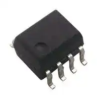
LBA716S
MOSFET RELAY, SPST-NO/NC, 1A, 60V, SMD
⚠️ Reference pricing provided. In case of supply shortages, we will connect you with our trusted procurement partners to ensure your project's continuity.
- Manufacturer: IXYS SEMICONDUCTOR
- Product type: MOSFET Solid State Relays
- Contact Form:SPST-NO (1 Form A), SPST-NC (1 Form B); Load Type:AC / DC; Load Voltage Max:60V; Load Current:1A; MOSFET Relay Package Style:DIP-8; Relay Mounting:Su
- Load Type: AC / DC
- Contact Form: SPST-NO (1 Form A), SPST-NC (1 Form B)
- Load Current: 1A
- Product Range: OptoMOS Series
- Relay Mounting: Surface Mount
- Relay Terminals: Gull Wing
- Load Voltage Max: 60V
- Isolation Voltage: 3.75kV
- I/O Capacitance Typ: 3pF
- On State Resistance Max: 0.4ohm
- MOSFET Relay Package Style: DIP-8
- Off State Leakage Current Max: 1µA
| Delivery and price | |
|---|---|
| Units per pack | 500 |
| Price | 4.45 € |
| Current stock | 10+ |
| Lead time | 30 days |
Datasheet

**LBA716 Dual Single-Pole OptoMOS[®] Relays Normally Open & Normally Closed** INTEGRATED CIRCUITS DIVISION |**Parameter**|**Rating**|**Units**| |---|---|---| |Load Voltage|60|V| |Load Current|1|Arms/ ADC| |On-Resistance(max)|0.4|| ## **Description** LBA716 is a 60V, 1A, 0.4 dual Solid State Relay integrating independent normally open (1-Form-A) and normally closed (1-Form-B) relays into a single package. It features a superior combination of low on-resistance and enhanced peak load current (5A max.) handling capability. ## **Features** - 3750Vrms Input/Output Isolation - Low Drive Power Requirements - Arc-Free With No Snubbing Circuits - No EMI/RFI Generation - Small 8-Pin Package - Flammability Rating UL 94 V-0 ## **Approvals** - UL Recognized Component: File # E76270 - CSA Certified Component: Certificate # 1175739 - EN/IEC 60950-1 Certified Component: Certificate available on our website - Surface Mount Version - Tape & Reel available ## **Applications** - Telecommunications ## **Ordering Information** |**Part #**|**Description**| |---|---| |LBA716|8-Pin DIP(50/Tube)| |LBA716S|8-Pin Surface Mount(50/Tube)| |LBA716STR|8-Pin Surface Mount(1000/Reel)| - Instrumentation - Multiplexers - Data Acquisition - Electronic Switching - I/O Subsystems ## **Switching Characteristics of Normally Open Devices** - Utility Meters (gas, oil, electric and water) - Medical Equipment-Patient/Equipment Isolation - Security - Aerospace - Industrial Controls **==> picture [125 x 81] intentionally omitted <==** **----- Start of picture text -----**<br> Form-A<br>IF<br>90%<br>10%<br>ILOAD<br>ton toff<br>**----- End of picture text -----**<br> ## **Pin Configuration** **==> picture [230 x 70] intentionally omitted <==** **----- Start of picture text -----**<br> 1 8<br>+ Control - Normally Closed<br>2 7 Normally Closed<br>– Control - Normally Closed<br>3 6<br>+ Control - Normally Open<br>Normally Open<br>4 5<br>– Control - Normally Open<br>**----- End of picture text -----**<br> ## **Switching Characteristics of Normally Closed Devices** **==> picture [122 x 79] intentionally omitted <==** **----- Start of picture text -----**<br> Form-B<br>IF<br>ILOAD<br>90%<br>10%<br>toff ton<br>**----- End of picture text -----**<br> **1** DS-LBA716-R04 **www.ixysic.com** **LBA716** INTEGRATED CIRCUITS DIVISION ## **Absolute Maximum Ratings @ 25ºC** |**Parameter**|**Ratings**|**Units**| |---|---|---| |BlockingVoltage|60|VP| |Reverse Input Voltage|5|V| |Input Control Current<br>Peak(10ms)|50|mA| ||1|A| |Input Power Dissipation1|150|mW| |Total Power Dissipation2|800|mW| |Isolation Voltage, Input to Output|3750|Vrms| |Operational Temperature|-40 to +85|°C| |Storage Temperature|-40 to +125|°C| _Absolute Maximum Ratings are stress ratings. Stresses in excess of these ratings can cause permanent damage to the device. Functional operation of the device at conditions beyond those indicated in the operational sections of this data sheet is not implied._ _Typical values are characteristic of the device at +25°C, and are the result of engineering evaluations. They are provided for information purposes only, and are not part of the manufacturing testing requirements._ > 1 Derate linearly 1.33 mW / **º** C > 2 Derate linearly 6.67 mW / **º** C ## **Electrical Characteristics @ 25ºC** |**Parameter**|**Conditions**|**Symbol**|**Min**|**Typ**|**Max**|**Units**| |---|---|---|---|---|---|---| |**Characteristics: Form-A (Normally Open)**||||||| |Load Current<br>Continuous<br>Peak<br>~~es~~|-<br>~~es~~|IL<br>~~es~~|-<br>~~es~~|-<br>~~es~~|1<br>~~es~~|Arms/ ADC<br>~~es~~| ||t<10ms<br>~~es~~|ILPK<br>~~es~~|-<br>~~es~~|-<br>~~es~~|±5<br>~~es~~|AP<br>~~es~~| |On-Resistance<br>~~es~~|IL=1A<br>~~es~~|RON<br>~~es~~|-<br>~~es~~|0.21<br>~~es~~|0.4<br>~~es~~|<br>~~es~~| |Off-State Leakage Current<br>~~rr~~|VL=60V<br>~~rr~~|ILEAK<br>~~rr~~|-<br>~~rr~~|-<br>~~rr~~|1<br>~~rr~~|A<br>~~rr~~| |Output Capacitance<br>~~rr~~|IF=0mA, V=50V, f=1MHz<br>~~rr~~|COUT<br>~~rr~~|-<br>~~rr~~|105<br>~~rr~~|-<br>~~rr~~|pF<br>~~rr~~| |Switching Speeds<br>Turn-On<br>Turn-Off<br>~~rr~~|IF=5mA, VL=10V<br>~~rr~~|ton<br>~~rr~~|-<br>~~rr~~|0.7<br>~~rr~~|5<br>~~rr~~|ms<br>~~rr~~| |||toff<br>~~rr~~|-<br>~~rr~~|0.09<br>~~rr~~|5<br>~~rr~~|| |Input Control Current to Activate|IL=1A|IF|-|-|2|mA| |Input Control Current to Deactivate<br>~~es~~|-<br>~~es~~|IF<br>~~es~~|0.1<br>~~es~~|-<br>~~es~~|-<br>~~es~~|mA<br>~~es~~| |**Characteristics: Form-B(Normally Closed)**<br>~~es~~||||||| |Load Current<br>Continuous<br>Peak<br>~~es~~|-<br>~~es~~|IL<br>~~es~~|-<br>~~es~~|-<br>~~es~~|0.5<br>~~es~~|Arms/ ADC<br>~~es~~| ||t<10ms<br>~~es~~|ILPK<br>~~es~~|-<br>~~es~~|-<br>~~es~~|±1.2<br>~~es~~|AP<br>~~es~~| |On-Resistance<br>~~es~~|IL=0.5A<br>~~es~~|RON<br>~~es~~|-<br>~~es~~|1.63<br>~~es~~|2<br>~~es~~|<br>~~es~~| |Off-State Leakage Current<br>~~a~~|VL=60V, IF=5mA<br>~~a~~|ILEAK<br>~~a~~|-<br>~~a~~|-<br>~~a~~|1<br>~~a~~|A<br>~~a~~| |Output Capacitance<br>~~a~~|IF=2mA, V=50V, f=1MHz<br>~~a~~|COUT<br>~~a~~|-<br>~~a~~|280<br>~~a~~|-<br>~~a~~|pF<br>~~a~~| |Switching Speeds<br>Turn-On<br>Turn-Off<br>~~a~~|IF=5mA, VL=10V<br>~~a~~|ton<br>~~a~~|-<br>~~a~~|0.58<br>~~a~~|5<br>~~a~~|ms<br>~~a~~| |||toff<br>~~a~~|-<br>~~a~~|0.76<br>~~a~~|5<br>~~a~~|| |Input Control Current to Activate<br>~~a~~|-<br>~~a~~|IF<br>~~a~~|-<br>~~a~~|-<br>~~a~~|2<br>~~a~~|mA<br>~~a~~| |Input Control Current to Deactivate|IL=0.5A|IF|0.1|-|-|mA| |**Common Characteristics: Form-A and Form-B**||||||| |Input Voltage Drop|IF=5mA|VF|0.9|1.2|1.5|V| |Reverse Input Current|VR=5V|IR|-|-|10|A| |Capacitance, Input to Output|VIO=0V, f=1MHz|CIO|-|3|-|pF| *NOTE: If both poles operate simultaneously, then load current must be derated so as not to exceed the package power dissipation value. R04 **www.ixysic.com** **2** **LBA716** INTEGRATED CIRCUITS DIVISION ## **Form-A RELAY PERFORMANCE DATA*** **==> picture [497 x 577] intentionally omitted <==** **----- Start of picture text -----**<br> Form-A Form-A Form-A<br>Typical LED Forward Voltage Drop Typical Turn-On Time Typical Turn-Off Time<br>(N=50, IF=5mA) (N=50, IF=5mA, IL=100mA) (N=50, IF=5mA, IL=100mA)<br>30 25 20<br>25 20<br>|e | 15 Pet | feel<br>20<br>15<br>15 10<br>10<br>10<br>5<br>5 5<br>0 =eA 0 hh 0 millsiis<br>1.220 1.225 1.230 1.235 1.240 1.245 0.57 0.61 0.65 0.69 0.73 0.77 0.077 0.082 0.087 0.092 0.097 0.102<br>LED Forward Voltage Drop (V) Turn-On Time (ms) Turn-Off Time (ms)<br>Form-A Form-A Form-A<br>Typical IF for Switch Operation Typical On-Resistance Typical Blocking Voltage<br>(N=50, IL=200mA) (N=50, IF=5mA, IL=1A) (N=50)<br>20 25 20<br>20 || | | i<br>15 15<br>15 | | | | i<br>10 10<br>10 ane<br>50 50 |||e Pei 50<br>0.65 0.69 0.73 0.77 0.81 0.85 0.206 0.207 0.208 0.209 0.210 0.211 65.5 66.0 66.5 67.0 67.5 68.0<br>LED Forward Current (mA) On-Resistance ( ) Blocking Voltage (VP)<br>Form-A Form-A Form-A<br>Typical IF for Switch Operation Typical Turn-On Time Typical Turn-Off Time<br>vs. Temperature vs. LED Forward Current vs. LED Forward Current<br>0.95 (IL=200mA) 1200 (IL=100mA) 77.8 (IL=100mA)<br>0.90 Pt || tT yb 1000 77.7 EEE<br>77.6<br>800<br>0.85 FERC - . 77.5 Fert<br>600<br>0.80 PTET LAL 400 77.4 2<br>77.3<br>0.75 COA 200 77.2 ——<br>0.70 +r] | | | 0 77.1 Tt<br>-40 -20 0 20 40 60 80 100 0 10 20 30 40 50 0 10 20 30 40 50<br>Temperature (ºC) LED Forward Current (mA) LED Forward Current (mA)<br>Form-A<br>Form-A Form-A Typical On-Resistance (AC)<br>Typical Turn-On Time vs. Temperature Typical Turn-Off Time vs. Temperature vs. Temperature<br>2.5 (IL=100mA) 90 (IL=100mA) 0.26 (IL=500mA, IF=5mA)<br>IF=2mA 85 eee eee 0.24 r | | | ht hth<br>2.0 80 IF=5mA 0.22<br>75<br>BSEEEER 0.20 FERED<br>1.5 70<br>65 26S IF=2mA 0.18 eee eee<br>1.0 60 tS 0.16 a<br>0.5 IF=5mA 5550 PotFESSdE dE dE SN 0.140.12 fr[Obart| | |<br>-40 -20 0 20 40 60 80 100 -40 -20 0 20 40 60 80 100 -40 -20 0 20 40 60 80 100<br>Temperature (ºC) Temperature (ºC) Temperature (ºC)<br>Device Count (N) Device Count (N) Device Count (N)<br>Device Count (N) Device Count (N) Device Count (N)<br>s) s)<br>LED Current (mA) Turn-On Time ( Turn-Off Time (<br>)<br>s)<br>Turn-On Time (ms) Turn-Off Time ( AC On-Resistance (<br>**----- End of picture text -----**<br> *Unless otherwise noted, data presented in these graphs is typical of device operation at 25ºC. For guaranteed parameters not indicated in the written specifications, please contact our application department. **www.ixysic.com** R04 **3** **LBA716** INTEGRATED CIRCUITS DIVISION ## **Form-A RELAY PERFORMANCE DATA*** **==> picture [511 x 586] intentionally omitted <==** **----- Start of picture text -----**<br> Form-A Form-A Form-A<br>Typical Load Current vs. Load Voltage Maximum Load Current vs. Temperature Typical Blocking Voltage<br>1.0 (IF=5mA) 1.2 (IF=5mA) 70 vs. Temperature<br>69<br>1.0<br>0.5 68<br>0.8<br>67<br>0.0 0.6 66<br>65<br>0.4<br>-0.5 64<br>0.2<br>63<br>-1.0 LEE 0.0 HAEee 62 ZEEE<br>-0.20 -0.15 -0.10 -0.05 0.00 0.05 0.10 0.15 0.20 -40 -20 0 20 40 60 80 100 -40 -20 0 20 40 60 80 100<br>Voltage (V) Temperature (ºC) Temperature (ºC)<br>Form-A<br>Typical Leakage vs. Temperature<br>Measured Across Pins 5 & 6 Form-A<br>20 (VL=60V) 6 Energy Rating Curve<br>5<br>15<br>4<br>10 32 T2 aTLaATT<br>5<br>1 a<br>0 Fe 0 201,<br>-40 -20 0 20 40 60 80 100 10 HTT s 100 s 1ms 10ms 100ms 1s 10s 100s<br>Temperature (ºC) Time<br>Form-B RELAY PERFORMANCE DATA*<br>Form-B Form-B Form-B<br>Typical LED Forward Voltage Drop Typical Turn-On Time Typical Turn-Off Time<br>30 (N=50, IF=5mA) 20 (N=50, IF=5mA, IL=100mA) 25 (N=50, IF=5mA, IL=100mA)<br>25 ‘TTETT 15 €6PTdhdlce!|hClUC@” 20 or<br>20<br>15<br>15 10<br>oon oe | coe 10<br>10<br>5<br>5 See | ee 5<br>0 ie 0 |) nae |) 0 0 ee|6©|—hLE |<br>1.220 1.225 1.230 1.235 1.240 1.245 0.507 0.530 0.553 0.576 0.599 0.622 0.63 0.67 0.71 0.75 0.79 0.83<br>LED Forward Voltage Drop (V) Turn-On Time (ms) Turn-Off Time (ms)<br>Form-B Form-B Form-B<br>Typical IF for Switch Operation Typical On-Resistance Typical Blocking Voltage<br>2520 | tl (N=50, IL=200mA) 20 (N=50, IF=0mA, IL=5mA) 20 (N=50, IF=5mA)<br>TT | 15 FT 15<br>15<br>10 10<br>10 P| , aTtan |<br>50 —Ets.fn. 50 _ _¥saaeale 50<br>0.16 0.17 0.18 0.19 0.20 0.21 1.49 1.53 1.57 1.61 1.65 1.69 75 76 77 78 79 80<br>LED Forward Current (mA) On-Resistance ( ) Blocking Voltage (VP)<br>)P<br>Current (A)<br>Load Current (A) Blocking Voltage (V<br>Load Current (A)<br>Leakage Current (nA)<br>Device Count (N) Device Count (N) Device Count (N)<br>Device Count (N) Device Count (N) Device Count (N)<br>**----- End of picture text -----**<br> *Unless otherwise noted, data presented in these graphs is typical of device operation at 25ºC. For guaranteed parameters not indicated in the written specifications, please contact our application department. R04 **www.ixysic.com** **4** **LBA716** INTEGRATED CIRCUITS DIVISION ## **Form-B RELAY PERFORMANCE DATA*** **==> picture [497 x 585] intentionally omitted <==** **----- Start of picture text -----**<br> Form-B Form-B Form-B<br>Typical Ivs. TemperatureF for Switch Operation vs. LED Forward CurrentTypical Turn-On Time vs. LED Forward CurrentTypical Turn-Off Time<br>0.40 (IL=100mA) 423 (IL=100mA) 2.5 (IL=100mA)<br>0.35 Pt | | tT 422 pot || 2.0<br>0.30 421<br>Pot | TE YT ee ET ee 1.5<br>0.25 420<br>Pt | | VA pote Tt<br>1.0<br>0.20 419<br>P| | TA pf] | |<br>0.15 418 0.5<br>Ppt | | Py ft |<br>0.10 417 0<br>-40 eT -20 | 0 ttt 20 40 60 1 80 100 0 ieee 10 20 30 40 50 0 10 20 30 40 50<br>Temperature (ºC) LED Forward Current (mA) LED Forward Current (ma)<br>Form-B Form-B<br>Typical Turn-On Time Typical Turn-Off Time Form-B<br>vs. Temperature vs. Temperature Typical On-Resistance vs. Temperature<br>800 (IL=100mA) 4.5 (IL=100mA) 1.8 (IF=0mA, IL=100mA)<br>700 SO 4.0 1.7<br>600 3.5 1.6<br>J PSXerrr 3.0 Eee IF=2mA eg Pee er<br>500 22N 1.5<br>e e 2.5 2 Se eee eee<br>400 1.4<br>300 FESS) IF=2mA 2.0 EERE 1.3 pee<br>1.5<br>200100 $e0ee IF=5mA 1.00.5 IF=5mA 1.21.1<br>ee ee ee<br>-40 -20 0 20 40 60 80 100 -40 -20 0 20 40 60 80 100 -40 -20 0 20 40 60 80 100<br>Temperature (ºC) Temperature (ºC) Temperature (ºC)<br>Form-B Form-B<br>Form-B Maximum Load Current Typical Blocking Voltage<br>Typical Load Voltage vs. Load Current vs. Temperature vs. Temperature<br>0.6 (IF=0mA) 0.6 (IF=0mA) 94 (IF=5mA)<br>0.4 Pt tt yy te 0.5 Pt tT tt 92 Pe<br>90<br>0.2 0.4<br>POP ENT 88 Eee<br>0.0 0.3<br>-0.2 CPECPREEOPPA 0.2 PNON 86 Be<br>84<br>-0.4 Pt at | tt yt 0.1 pt tt TT 82 7 Ee<br>-0.6 PPT LTT Tt 0.0 Pt ot EE tT 80 Po<br>-1.0 -0.8 -0.5 -0.3 0.0 0.3 0.5 0.8 1.0 -40 -20 0 20 40 60 80 100 -40 -20 0 20 40 60 80 100<br>Voltage (V) Temperature (ºC) Temperature (ºC)<br>Form-B<br>Typical Leakage vs.Temperature<br>Measured Across Pins 7&8 Form-B<br>350300 C (IF=5mA, V TT L=60V) 1.51.3 Energy Rating Curve<br>250<br>1.1<br>200 Sees= | ai<br>0.9<br>150 ne ae AIAN<br>100500 pyeSeSoemerwan 0.70.50.3 SUTtt [tit] ATTT it! a<br>-40 -20 0 20 40 60 80 100 10 s 100 s 1ms 10ms 100ms 1s 10s 100s<br>Temperature (ºC) Time<br>s)<br>LED Current (mA) Turn-On Time ( Turn-Off Time (ms)<br>s) )<br>Turn-On Time ( Turn-Off Time (ms) On-Resistance (<br>)P<br>Current (A)<br>Load Current (A) Blocking Voltage (V<br>Load Current (A)<br>Leakage Current (nA)<br>**----- End of picture text -----**<br> *Unless otherwise noted, data presented in these graphs is typical of device operation at 25ºC. For guaranteed parameters not indicated in the written specifications, please contact our application department. **www.ixysic.com** R04 **5** **LBA716** INTEGRATED CIRCUITS DIVISION ## **Manufacturing Information** ## **Moisture Sensitivity** All plastic encapsulated semiconductor packages are susceptible to moisture ingression. IXYS Integrated Circuits classifies its plastic encapsulated devices for moisture sensitivity according to the latest version of % the joint industry standard, **IPC/JEDEC J-STD-020** , in force at the time of product evaluation. We test all of our products to the maximum conditions set forth in the standard, and guarantee proper operation of our devices when handled according to the limitations and information in that standard as well as to any limitations set forth in the information or standards referenced below. Failure to adhere to the warnings or limitations as established by the listed specifications could result in reduced product performance, reduction of operable life, and/or reduction of overall reliability. This product carries a Moisture Sensitivity Level (MSL) classification as shown below, and should be handled according to the requirements of the latest version of the joint industry standard **IPC/JEDEC J-STD-033** . |**Device**<br>~~EE~~|**Moisture Sensitivity Level (MSL) Classifi cation**<br>~~EE~~| |---|---| |LBA716 / LBA716S<br>~~EE~~|MSL 1<br>~~EE~~| ## **ESD Sensitivity** This product is **ESD Sensitive** , and should be handled according to the industry standard **JESD-625** . ## **Soldering Profile** Provided in the table below is the Classification Temperature (TC) of this product and the maximum dwell time the body temperature of this device may be (TC - 5)ºC or greater. The classification temperature sets the Maximum Body Temperature allowed for this device during lead-free reflow processes. For through-hole devices, and any other processes, the guidelines of **J-STD-020** must be observed. |**Device**<br>~~—~~|**Classifi cation Temperature (Tc)**|**Dwell Time (tp)**|**Max Refl ow Cycles**| |---|---|---|---| |LBA716<br>~~—~~|250ºC|30 seconds|1| |LBA716S<br>~~—~~|250ºC|30 seconds|3| ## **Board Wash** IXYS Integrated Circuits recommends the use of no-clean flux formulations. Board washing to reduce or remove flux residue following the solder reflow process is acceptable provided proper precautions are taken to prevent damage to the device. These precautions include, but are not limited to: using a low pressure wash and providing a follow up bake cycle sufficient to remove any moisture trapped within the device due to the washing process. Due to the variability of the wash parameters used to clean the board, determination of the bake temperature and duration necessary to remove the moisture trapped within the package is the responsibility of the user (assembler). Cleaning or drying methods that employ ultrasonic energy may damage the device and should not be used. Additionally, the device must not be exposed to flux or solvents that are Chlorine- or Fluorine-based. R04 **www.ixysic.com** **6** **LBA716** INTEGRATED CIRCUITS DIVISION ## **Mechanical Dimensions** ## **LBA716** **==> picture [415 x 171] intentionally omitted <==** **----- Start of picture text -----**<br> 9.652 ± 0.381 7.620 ± 0.254 PCB Hole Pattern<br>2.540 ± 0.127 (0.380 ± 0.015) (0.300 ± 0.010)<br>(0.100 ± 0.005) 8-0.800 DIA. 2.540 ± 0.127<br>fy (8-0.031 DIA.) (0.100 ± 0.005)<br>9.144 ± 0.508<br>6.350 ± 0.127 (0.360 ± 0.020)<br>(0.250 ± 0.005) _ | : Ly ;<br>Pin 1 3.302 ± 0.051<br>0.457 ± 0.076 (0.130 ± 0.002)<br>(0.018 ± 0.003) 7.239 TYP. 7.620 ± 0.127<br>(0.285) (0.300 ± 0.005)<br>7.620 ± 0.127<br>es 4.064 TYP(0.160) be 0.254 ± 0.0127 ij] (0.300 ± 0.005)<br>(0.010 ± 0.0005)<br>r m Dimensions<br>0.813 ± 0.102 mm<br>t (0.032 ± 0.004) — (inches)<br>**----- End of picture text -----**<br> ## **LBA716S** > 9.652 ± 0.381 **PCB Land Pattern** (0.380 ± 0.015) 0.635 ± 0.127 2.540 ± 0.127 3.302 ± 0.051 (0.025 ± 0.005) 2.54 (0.100 ± 0.005) (0.130 ± 0.002) (0.10) ~~hid = rt~~ 6.350 ± 0.127 9.525 ± 0.254 (0.250 ± 0.005) (0.375 ± 0.010) 1.65 8.90 (0.0649) (0.3503) 7.620 ± 0.254 Pin 1 (0.300 ± 0.010) ~~ce~~ 0.457 ± 0.076 0.254 ± 0.0127 (0.018 ± 0.003) (0.010 ± 0.0005) 0.65 (0.0255) 4.445 ± 0.127 (0.175 ± 0.005) Dimensions 0.813 ± 0.102 mm ~~or~~ (0.032 ± 0.004) - (inches) **www.ixysic.com** R04 **7** **LBA716** INTEGRATED CIRCUITS DIVISION **==> picture [451 x 182] intentionally omitted <==** **----- Start of picture text -----**<br> LBA716STR Tape & Reel<br>330.2 DIA.<br>(13.00 DIA.)<br>Top Cover W=16.00<br>Tape Thickness Bo=10.30 (0.63)<br>0.102 MAX. (0.406)<br>(0.004 MAX.)<br>Ao=10.30 P1=12.00<br>K0 =4.90 (0.406) (0.472)<br>(0.193)<br>K1 =4.20 User Direction of Feed<br>Embossed Carrier (0.165) Dimensions<br>mm<br>onoe NOTES: (inches)<br>1. Dimensions carry tolerances of EIA Standard 481-2<br>Embossment 2. Tape complies with all “Notes” for constant dimensions listed on page 5 of EIA-481-2<br>**----- End of picture text -----**<br> ## **For additional information please visit our website at: www.ixysic.com** IXYS Integrated Circuits makes no representations or warranties with respect to the accuracy or completeness of the contents of this publication and reserves the right to make changes to specifications and product descriptions at any time without notice. Neither circuit patent licenses nor indemnity are expressed or implied. Except as set forth in IXYS Integrated Circuits' Standard Terms and Conditions of Sale, IXYS Integrated Circuits assumes no liability whatsoever, and disclaims any express or implied warranty, relating to its products including, but not limited to, the implied warranty of merchantability, fitness for a particular purpose, or infringement of any intellectual property right. The products described in this document are not designed, intended, authorized or warranted for use as components in systems intended for surgical implant into the body, or in other applications intended to support or sustain life, or where malfunction of IXYS Integrated Circuits' product may result in direct physical harm, injury, or death to a person or severe property or environmental damage. IXYS Integrated Circuits reserves the right to discontinue or make changes to its products at any time without notice. Specification: DS-LBA716-R04 ©Copyright 2018, IXYS Integrated Circuits OptoMOS[®] is a registered trademark of IXYS Integrated Circuits All rights reserved. Printed in USA. **8** 6/25/2018
Updated at April 22, 2026
About Novapart
Novapart is a B2B electronic component broker specialising in stock shortages and cost reduction. We source hard-to-find parts and identify compliant alternatives across a catalogue of 410,000+ components from 500+ manufacturers.
Learn more →Stock Shortage Specialist
When a component is unavailable, discontinued or has an unacceptable lead time, we tap into our network of vetted European and Asian distributors to source what you need — without compromising on quality or traceability.
Request a quote →Compliant Alternatives
We identify pin-to-pin, electrically equivalent substitutes that meet the same certifications (RoHS, AEC-Q100, REACH) as your original specification — validated against datasheets, not just part numbers. Often at a lower cost.
BOM Analysis service →