
Image not available
Illustrative purposes only

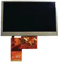
K430WQA-V4-F
LCD MODULE, 4.3", 480X272, TOUCH SCREEN
⚠️ Reference pricing provided. In case of supply shortages, we will connect you with our trusted procurement partners to ensure your project's continuity.
- Manufacturer: KENTEC DISPLAY
- Product type: TFT LCD Displays
- Display Size:4.3"; Resolution:480 x 272; VGA Size:-; Display Orientation:Landscape; Display Appearance:RGB; Logic Voltage:3.3V; Interface Type:RGB; Display Bri 82T4652
- Resolution: 480 x 272
- Touchscreen: Resistive Touch
- Interface Type: RGB
| Delivery and price | |
|---|---|
| Units per pack | 288 |
| Price | 13.69 € |
| Current stock | 10+ |
| Lead time | 30 days |
Datasheet

**FS-K430WQA-V4-F 13/Jul/2011**

**PAGE 1 OF 20**

**K430WQA-V4-F**

Standard LCD Module **Product** 480 x RGB x 272 Dots 4.3” 16.7M colors TFT display Wide temperature With white LED backlight With touch screen

Kentec Electronics (Displays) Limited URL: http://www.kentecdisplay.com E-mail: t.liang@kentecdisplay.com ; mf.zou@kentecdisplay.com

**FS-K430WQA-V4-F 13/Jul/2011 PAGE 2 OF 20**

|~~i~~<br>VW|~~i~~ KENTEC<br>VW DISPLAY|**PAGE 2 OF 20**|
|---|---|---|
||**CONTENTS**||
|||Page No.|
|1.|DOCUMENT REVISION HISTORY|3|
|2.|GENERAL DESCRIPTION|4|
|3.|MECHANICAL SPECIFICATIONS|4|
|4.|INTERFACE SIGNALS|6|
|5.|ABSOLUTE MAXIMUM RATINGS|7|
|6.|ELECTRICAL SPECIFICATIONS|7|
|7.|OPTICAL CHARACTERISTICS|8|
|8.|TIMING CHARACTERISTICS|10|
|9.|RELIABILITY TEST ITEM|13|
|10.|SUGGESTIONS FOR USING LCD MODULES|13|
|11.|INSPECTION STANDARD|16|
|12.|PACKING(REFERENCE ONLY)|20|


**FS-K430WQA-V4-F 13/Jul/2011**

**PAGE 3 OF 20**

## **1. Document revision history :**

|DOCUMENT<br>REVISION|DATE|DESCRIPTION|PREPARED<br>BY|APPROVED<br>BY|
|---|---|---|---|---|
|01|2010.11.22|First Release.|MF Zou||
|02|2011.07.13|Updated the LED backlight driving current|XW Lee||


**FS-K430WQA-V4-F 13/Jul/2011**

**PAGE 4 OF 20**

## **2. General Description**

- 4.3”(diagonal), 480 x RGB x 272 dots, 16.7M colors, Normal white TN, TFT LCD module.

- Viewing Direction: 6 o’clock.

- RGB 24-bits

- With internal voltage booster.

- Logic voltage: 3.3V (typ.).

- With 4-wire resistive touch screen

## **3. Mechanical Specifications**

The mechanical detail is shown in Fig. 1 and summarized in Table 1 below.

## Table 1

|||Table 1||
|---|---|---|---|
|Parameter||Specifications|Unit|
|Outline dimensions||105.5(W) x 67.2(H) x 4.1(D)<br>(Exclude FPC,cables of backlight)|mm|
|Color TFT<br>480xRGBx272|View area|97.9(W)x 56.7(H)|mm|
||TP active area|96.7(W)x 55.5(H)|mm|
||LCD active area|95.04(W)x 53.86(H)|mm|
||Displayformat|480 x RGB x 272|dots|
||Color configuration|RGB Side-stripes|-|
||Dot size|0. 198(W)x 0.198(RGB)|mm|
|Weight||TBD|grams|


**FS-K430WQA-V4-F 13/Jul/2011**

**PAGE 5 OF 20**

**==> picture [325 x 419] intentionally omitted <==**

**----- Start of picture text -----**<br>
&<br>a<br>aval fae<br>x * 2<br>> > a2 154 15<br>“x “x<br>“- “:<br>a /<br>ie,<br>+<br>3<br>= BH<br>°'. i<br>P PLE<br>rr 39 0 '0 ><br>~ +8610 5<br>n<br>Zz<br>oO Lu<br>° =<br>| ite) Oo 5<br>° 2 2<br>RSSRSSeSS 3 oO ina)<br>fo GO] F L) IEO SSS S Ressy QO4 ~- © Lawt<br> _ >| EHR SS : re )<br>ieReK SSRRSS‘| L i z¥ a G GS S Poey S«®7 w<br>RB SSy & 2 r Oo ~=<br>R BBN . ao ° t e)<br>K SSS 2 i Of Ze<br>| y k soc F FP 8<br>Ree Ya Page<br>H—f il—————————————— | _{ |____}x _l RSS 2%30S BogoH woe 4 F >~_ VeeO eOoo—~ nSsrFoC=A etaz°Wueo)Fa> ao = a z 2<br>C ¥ /' 9 )98'EGS———____ 4 ~OFuig o o t<br>«CY v y d d l Lo0s’>¢¢-———-G'SS + N WAaONnda O MNraF a v u=<br>K<br>LED CIRCUIT<br>A<br>STIFFENER<br>TP front<br>CONTACT SIDE<br>RGB)*272<br>480( Components Area  H=1.5 Max.<br>RGB<br>▽<br>)<br>**----- End of picture text -----**<br>


**==> picture [140 x 11] intentionally omitted <==**

**----- Start of picture text -----**<br>
Figure 1: Outline Drawing<br>**----- End of picture text -----**<br>


**FS-K430WQA-V4-F 13/Jul/2011**

**PAGE 6 OF 20**

## **4.  Interface signals**

## Table 2: Pin assignment

**FS-K430WQA-V4-F 13/Jul/2011 PAGE 7 OF 20**

## **5. Absolute Maximum Ratings**

## **5.1 Electrical Maximum Ratings – for IC Only**

Table 3: Electrical Maximum Ratings – for IC

|Parameter|Symbol|Min.|Max.|Unit|Note|
|---|---|---|---|---|---|
|Supplyvoltage|VCC|-0.3|+4.0|V|1|
|Input voltage|AVDD|-0.3|+5.0|V||


1.VCC, GND must be maintained.

- 2.The modules may be destroyed if they are used beyond the absolute maximum ratings.

## **5.2 Environmental Condition**

|Item|Operating<br>temperature<br>(Topr)|Operating<br>temperature<br>(Topr)|Storage<br>temperature<br>(Tstg)<br>(Note 1)|Storage<br>temperature<br>(Tstg)<br>(Note 1)|Remark|
|---|---|---|---|---|---|
||Min.|Max.|Min.|Max.||
|Ambient temperature|-20°C|+70°C|-30°C|+80°C|Dry|
|Humidity (Note 1)|80% max. RH for Ta≤40°C<br>< 50% RH for 40°C < Ta≤Maximum operatingtemperature||||No<br>condensation|


## **6. Electrical Specifications**

## **Typical Electrical Characteristics**

At Ta = 25 ° C, VCC=IOVCC= 3.3V, GND=0V.

|||Table 5|||||
|---|---|---|---|---|---|---|
|Parameter|Symbol|Conditions|Min.|Typ.|Max.|Unit|
|Supplyvoltage(logic)|VDD-GND||3.0|3.3|3.6|V|
|Input signal voltage|VIH||**0.7VDD**|-|VDD|V|
||VIL||**GND**|-|0.3VDD|V|
|Supply current<br>(Logic & LCD)|IDD|VDD=3.3V|-|15|19|mA|
|LED Backlight<br>Supply current|ILED|Forward voltage<br>VLED = ~13.5V<br>@ 40mA|-|36|40|mA|


Note (1): LED backlight required current constant power supply. LED circuit was in 2 chain parallel and with 4 LEDs serial per chain. LED backlight power consumption is 0.55W.

**FS-K430WQA-V4-F 13/Jul/2011 PAGE 8 OF 20**

## **7. Optical Characteristics**

Table 7: Optical specifications

Specifications Items Symbol Condition ~~eeee~~ Min. Typ. Max.[Unit] Contrast Ratio CR 150 300 - - ~~ee a ee~~ Response Time TR - 15 30 ms TF - 35 50 ms ~~a fC eee aee~~ Red XR 0.604 0.624 0.644 - ~~i;~~ YR ~~ee~~ 0.302 0.322 0.342 - ~~fC a~~ Green XG 0.268 0.288 0.308 - ~~i;|~~ YG ~~**a**~~ 0.540 0.560 0.580 - Chromaticity Blue XB 0.127 0.147 0.167 - YB 0.097 0.117 0.137 - ~~_ _— a~~ White XW - 0.307 - - ~~|~~ ~~**|**~~ YW ~~**a**~~ - 0.328 ~~ee ee~~ - - φ 1(3 o’clock) - 45 - Hor. ~~|~~ ~~**|**~~ φ 2(9 o’clock) Center ~~Pt~~ ~~**a**~~ - 45 - Viewing angle deg. θ 2(12 o’clock) CR=10 - 15 - Ver. θ 1(6 o’clock) - 35 - ~~_ _— 4~~ NTSC ratio 61.5 % ~~es ees|rs rsP|rs es~~ Note 1: Definition of Contrast Ratio (CR):

Note

The contrast ratio can be calculated by the following expression. Contrast Ratio (CR) = L63 / L0

L63: Luminance of gray level 63

L0: Luminance of gray level 0

CR = CR (10)

CR (X) is corresponding to the Contrast Ratio of the point X at Figure in Note 5. Note 2: Definition of Response Time (TR, TF):

**==> picture [44 x 12] intentionally omitted <==**

**----- Start of picture text -----**<br>
Figure 3<br>**----- End of picture text -----**<br>


**FS-K430WQA-V4-F 13/Jul/2011 PAGE 9 OF 20**

Note 3: Viewing Angle

Figure 4 The above “Viewing Angle” is the measuring position with Largest Contrast Ratio; not for good image quality. View Direction for good image quality is 6 O’clock. Module maker can increase the “Viewing Angle” by applying Wide View Film.

## Note 4: Measurement Set-Up:

The LCD module should be stabilized at a given temperature for 20 minutes to avoid abrupt temperature change during measuring. In order to stabilize the luminance, the measurement should be executed after lighting Backlight for 20 minutes in a windless room.

Figure 5

**FS-K430WQA-V4-F 13/Jul/2011**

**PAGE 10 OF 20**

## **8. AC Characteristics**

**FS-K430WQA-V4-F**

**13/Jul/2011**

**PAGE 11 OF 20**

**FS-K430WQA-V4-F 13/Jul/2011**

**PAGE 12 OF 20**

**FS-K430WQA-V4-F 13/Jul/2011**

**PAGE 13 OF 20**

## **9. Reliability Test Item**

|**Test Item**|**Test  Condition**<br>℃|**Test result determinant gist**|
|---|---|---|
|High temperature storage|80±3<br>;<br>℃96H<br>℃|the inspection of<br>appearance and  function<br>character.|
|Low temperature storage|-30±3<br>;<br>℃120H<br>℃<br>℃||
|High temperature<br>/humidity storage|50<br>±<br>℃3<br>,90%±3%RH;<br>℃<br>96H<br>℃||
|High temperature operation|70±3<br>;96H<br>℃<br>℃|no objection of  the<br>function character; no fatal<br>objection of the appearance.|
|Low temperature operation|-20±3<br>;96H<br>℃<br>℃℃||
|Temperature Shock|-20±3℃,30min? 70±3℃,<br>30min;10cycle|inspect the objections<br>appearance、function & the<br>whole structure|


## **10. Suggestions for using LCD modules**

## **10.1 Handling of LCM**

1. The LCD screen is made of glass. Don't give excessive external shock, or drop from a high place.

2. If the LCD screen is damaged and the liquid crystal leaks out, do not lick and swallow. When the liquid is attach to your hand, skin, cloth etc, wash it off by using soap and water thoroughly and immediately.

3. Don't apply excessive force on the surface of the LCM.

4. If the surface is contaminated ,clean it with soft cloth. If the LCM is severely contaminated , use Isopropyl alcohol/Ethyl alcohol to clean. Other solvents may damage the polarizer . The following solvents is especially prohibited: water , ketone Aromatic solvents etc.

5. Exercise care to minimize corrosion of the electrode. Corrosion of the electrodes is accelerated by water droplets, moisture condensation or a current flow in a high-humidity environment.

6. Install the LCD Module by using the mounting holes. When mounting the LCD module make sure it is free of twisting, warping and distortion. In particular, do not forcibly pull or bend the I/O cable or the backlight cable.

7. Don’t disassemble the LCM.

8. To prevent destruction of the elements by static electricity, be careful to maintain an optimum work

**FS-K430WQA-V4-F 13/Jul/2011 PAGE 14 OF 20**

environment.

   - Be sure to ground the body when handling the LCD modules.

   - Tools required for assembling, such as soldering irons, must be properly grounded.

   - To reduce the amount of static electricity generated, do not conduct assembling and other work under dry conditions.

   - The LCD module is coated with a film to protect the display surface. Exercise care when peeling off this protective film since static electricity may be generated.

9. Do not alter, modify or change the the shape of the tab on the metal frame. 10. Do not make extra holes on the printed circuit board, modify its shape or change the positions of components to be attached.

11. Do not damage or modify the pattern writing on the printed circuit board. 12. Absolutely do not modify the zebra rubber strip (conductive rubber) or heat seal connector 13. Except for soldering the interface, do not make any alterations or modifications with a soldering iron. 14. Do not drop, bend or twist LCM.

## **10.2 Cautions for installing and assemabling if the module has Touch Panel**

1. Use a buffer material (Gasket) between the touch panel and Front-case to protect damage and wrong operating. The dimension of the buffer material’s edge between the TP V.A. edge is Min. 0.3mm. 2. We recommend to design a case that it can’t over the boundary of the active area Max. 0.5mm in order to prevent an operation at outside of the active area which can’t guarantee the specified durability, because operation at the outside of the active area cause serious damage of a transparent. 3. When design case for installing Module, you would consider give a distance about 0.2 ± 0.15mm between the module edge to case inside. 4. The corners of the product are not chamfered. When positioning and fixing the product on the case, we sugguest that you would provide a R part on the conner of the case so as not to apply load on the corner of the transparent module.

**FS-K430WQA-V4-F 13/Jul/2011 PAGE 15 OF 20**

**==> picture [461 x 209] intentionally omitted <==**

**----- Start of picture text -----**<br>
mront ase Max. 0.5mm -)<br>机壳<br>[ oN Touch Panel ©<br>owes 触摸屏<br>Buffer material(gasket) P asse erren eae a |<br>缓冲材料垫圈 ( ) / KeKeRe Ree RE EKE<br>Insulation area Yfffffff<br>绝缘油墨区域<br>. . / \<br>背光<br>TP Ac tive area( 驱动区域边缘<br>0.2+0.15mm TP View area( 可视区域边缘 )<br>**----- End of picture text -----**<br>


## **10.3 Storage**

1. Store in an ambient temperature of 5 to 45 ° C, and in a relative humidity of 40% to 60%. Don't expose

- to sunlight or fluorescent light.

2. Storage in a clean environment, free from dust, active gas, and solvent.

3. Store in antistatic container.

**FS-K430WQA-V4-F 13/Jul/2011 PAGE 16 OF 20**

## **11. Inspection Standard**

This specification is made to be used as the standard acceptance/rejection criteria for Color mobile phone LCM with touch pannel.

## **11.1 Sample plan and Inspection condition**

## 11.1.1 Sample plan

Sampling plan according to MIL-STD-105E , normal level 2 and based on: Major defect: AQL 0.65;

Minor defect: AQL 1.5.

## 11.1.2 Inspection condition

Viewing distance for cosmetic inspection is about 30cm with bare eyes, and under an environment of

20~40W light intensity, all directions for inspecting the sample should be within 45 against perpendicular line.

## **11.2 Definition of inspection zone in LCD**

Inspection zones in an LCD

Zone A: character/Digit area;

Zone B: viewing area except Zone A (ZoneA+ZoneB=minimum Viewing area);

Zone C: Outside viewing area (invisible area after assembly in customer’s product);

Note: As a general rule, visual defects in Zone C are permissible, when it is no trouble for quality and assembly of customer’s product. Defects are classified as major defects and minor defects according to the degree of defectiveness defined herein.

## **11.3 Major defects and Minor defects**

11.3.1 Major defects

A major defect is a defect that is likely to result in failure, or to reduce the usability of the product for its intended purpose.

11.3.1.1 Abnormal operation: modules cannot display normally;

**FS-K430WQA-V4-F 13/Jul/2011 PAGE 17 OF 20**

## 11.3.1.2 Line defect;

- 11.3.1.3 There is serious distortion or sharp burr on mechanical housing;

- 11.3.1.4 Glass breakage.

- 11.3.2 Minor defects:

A minor defect is a defect that is not likely to reduce the usability of the product for its intended purpose.

- 11.3.2.1 Dot defect:

11.3.2.1.1 Inspection pattern : Full white, full black, red, green and blue screens; 11.3.2.1.2 Criteria :(acceptable);

**==> picture [368 x 137] intentionally omitted <==**

**----- Start of picture text -----**<br>
1/5<br>Sub-pixel<br>3/5<br>? area<br>? area<br>Se 1/5<br>had [DG] ed<br>1/5  3/5  1/5<br>**----- End of picture text -----**<br>


- Note: 1. Dot defect is defined as the defective area of the dot area is larger than 50% of the dot area . And the bright dot defect must be visible through 5% ND filter.

   2. Except for the allowed numbers of adjacent dots, the distance between dot defects should be more than 3mm apart.

- 11.3.2.1.3 The definitions of the inner display area and outer display area.

## **11.4 Inspection standards table:**

11.4.1 Major defect

|Item<br>No.|Items to be|Inspection Standard|Classification<br>of defects|
|---|---|---|---|
|11.4.1.1|All functional<br>defects|1) No display<br>2) Display abnormally<br>3) Missing vertical/horizontal segment<br>4) Short circuit<br>5) Back-light no lighting, flickering and<br>abnormal lighting.|Major|
|11.4.1.2|Missing|Missingcomponent||
|11.4.1.3|Outline<br>dimension|Overall outline dimension beyond the<br>drawing is not allowed.||
|11.4.1.4|linearity|No more than 1.5%||


11.4.2 Cosmetic Defect (spot defect)

**FS-K430WQA-V4-F 13/Jul/2011**

**PAGE 18 OF 20**

|Item No<br>~~a~~<br>~~|~~|Itemsto be<br>~~a ee~~<br>~~|~~|Inspection Standard<br>~~ee~~<br>~~===~~|Inspection Standard<br>~~ee~~<br>~~===~~|Inspection Standard<br>~~ee~~<br>~~===~~|Inspection Standard<br>~~ee~~<br>~~===~~|Inspection Standard<br>~~ee~~<br>~~===~~|Inspection Standard<br>~~ee~~<br>~~===~~|Classification<br>of defects<br>~~ee~~<br>~~===~~|
|---|---|---|---|---|---|---|---|---|
|11.4.2.1<br>~~a~~<br>~~|~~|**Clear Spots**<br>Black and<br>white<br>Spot defect<br>Pinhole,<br>Foreign<br>Particle,<br>polarizer<br>Dirt<br>~~a ee~~<br>~~|~~|For dark/white spot, sizeF is defined<br>as F =( x +y )/2<br>~~ee~~<br>~~===~~||||||Minor<br>~~ee~~<br>~~===~~|
||||Zone<br>Size(mm) <br>~~===~~|AcceptableQty<br>~~===~~|||~~===~~|Minor<br>~~===~~|
|||||A<br>~~===~~|B<br>~~===~~|C<br>~~===~~|||
||||F =0.1<br>~~===~~|Ignore<br>~~===~~||Ignore<br>~~===~~|||
||||0.10< F =0.15<br>~~===~~|2<br>~~===~~|||||
||||0.15< F =0.20<br>~~===~~|1<br>~~===~~|||||
||||F> 0.20<br>~~===~~|0<br>~~===~~|||||
|11.4.2.2<br>~~|~~|**Clear Spots**<br>TP Dirt<br>~~| ~~||Zone<br>Size(mm)<br> ~~===~~|AcceptableQty<br>~~===~~|||~~===~~|Minor<br>~~===~~|
|||||A|B|C|||
||||F =0.1|Ignore||Ignore|||
||||0.10< F =0.15|2|||||
||||0.15< F =0.25|1|||||
||||F> 0.25|0|||||
|11.4.2.3|**Dim Spots**<br>Circle<br>shaped and<br>dim edged<br>defects||Zone<br>Size(mm)|AcceptableQty||||Minor|
|||||A|B|C|||
||||F =0.2|Ignore||Ignore|||
||||0.20< F =0.4|2|||||
||||0.4< F =0.6|1|||||
||||F> 0.6|0|||||
|11.4.2.4|**Dot defect**|dot =sub-pixel<br>AcceptableQty<br>I<br>II<br>Bright dot<br>0<br>2<br>Dark dot<br>1<br>2<br>The distance of twopoint >5mm||||||Minor|


**FS-K430WQA-V4-F 13/Jul/2011**

**PAGE 19 OF 20**

||||If the scratch can be seen after mobile phone cover assembling or in the|||
|---|---|---|---|---|---|
||||operating condition, judge by the line defect of 11.4.3.1. If the scratch can|operating condition, judge by the line defect of 11.4.3.1. If the scratch can||
||||be seen only in non-operating condition or some special angle, judge by|||
|11.4.3.2<br>**Dim line**<br>**defect**<br>Polarizer<br>&BL scratch<br>TP film<br>scratch<br>11.4.3.3<br>Polarize<br>Air<br>bubble<br>ry|||the following.<br>Size(mm)<br>Acceptable Qty<br>zone<br>L(Length)<br>W(Width)<br>A<br>B<br>C<br>Ignore<br>W=0.02<br>Ignore<br>L=3.0<br>0.02< W=0.03<br>2<br>L=2.0<br>0.03< W=0.05<br>1<br>W> 0.05<br>Define as spot defect<br>Ignore<br>Air bubbles betweenglass &polarizer<br>Acceptable Qty<br> <br>A<br>B<br>C<br>F =0.2<br>Ignore<br>0.20< F =0.3<br>2<br>0.3< F =0.5<br>1<br>F> 0.5<br>0<br>Ignore<br>~~ee~~<br>~~Po~~<br>~~a ee eee~~<br>~~ee~~<br>~~OSee~~||Minor<br>Minor|
||11.4.4 ChippingDefect||Defect|||
||Item No<br>Items to be<br>Inspection Standard<br>Classification<br>of defects<br>~~ee~~|||||
||||Chips on corner|||
||||**A:LCD Glass defect**|||
||||X<br>Y<br>Z|||
||||=0.2<br>=S<br>Disregard|||
||11.4.4.1|Glass<br>defect|Notes: S=contact pad length<br>Chips on the corner of terminal shall not be allowed to extend into the<br>ITO pad or expose perimeter seal.||Minor|
||||**B:TP Glass defect**|||
||||X<br>Y<br>Z|||
||||=3.0<br>=3.0<br>Disregard|||


**FS-K430WQA-V4-F 13/Jul/2011 PAGE 20 OF 20**

||||Usual surface cracks||||||
|---|---|---|---|---|---|---|---|---|
||||**A:LCD Glass defect**||||||
||||eee ea,<br>oe||||||
||||X<br>Y|Z|||||
||||=3.0<br><Inner border line of the seal<br>Disregard||||||
||||**B:TP Glass defect**||||||
||||iv||||||
||||X<br>Y<br>Z<br>=6.0<br>=2.0<br>Disregard<br>a<br>—~~——~~||||||
||||Crack: Cracks tend to break are not allowed.||||||
|11.4.5 Parts Defect|||||||||
|Item No|Items to be||Inspection Standard|||||Classification<br>of defects|
||||、<br>1<br>Not allow IC and FPC/heat-seal lead width is more than||||||
|11.4.5.1|Parts contra<br>position||50% beyond lead pattern.<br>、<br>2<br>Not allow chip or solder component is off center more than||Not allow chip or solder component is off center more than|||Major|
||||50% of thepad outline.||||||
||||According to the <Acceptability of electronic||||||
|11.4.5.2|SMT||assemblies>IPC-A-610C class 2 standard. Component missing|||||Major|
||||or function defect are Major defect,the others are Minor defect.||||||
||||1 Illumination source flickers when lit.||||||
|11.4.5.3|Backlight<br>elements||2 Spots or scratches that appear when lit must be judged using<br>LCD spot, lines and contamination standards.|||||Major|
||||3 Backlight doesn’t light or color is wrong||||||
||||1 No unmelted solder paste may be present on the FPC||||||
|11.4.5.4|Soldering||2 No cold solder joints, missing solder connections, oxidation<br>or icicle.|||||Major|
||||3 No short circuits in components on FPC||||||


**11. Packing T.B.D.**
Updated at April 23, 2026
About Novapart
Novapart is a B2B electronic component broker specialising in stock shortages and cost reduction. We source hard-to-find parts and identify compliant alternatives across a catalogue of 410,000+ components from 500+ manufacturers.
Learn more →Stock Shortage Specialist
When a component is unavailable, discontinued or has an unacceptable lead time, we tap into our network of vetted European and Asian distributors to source what you need — without compromising on quality or traceability.
Request a quote →Compliant Alternatives
We identify pin-to-pin, electrically equivalent substitutes that meet the same certifications (RoHS, AEC-Q100, REACH) as your original specification — validated against datasheets, not just part numbers. Often at a lower cost.
BOM Analysis service →