


JW1P1
Relay Socket, Through Hole, Quick Connect
- Manufacturer: PANASONIC
- Product type: Relay Sockets
- Socket Mounting: Through Hole
- Socket Terminals: Quick Connect
| Delivery and price | |
|---|---|
| Units per pack | 100 |
| Price | 1.06 € |
| Current stock | 10+ |
| Lead time | 30 days |
**VDE** wE A ~~WwW~~ @ © ©
JW
## **COMPACT PC BOARD POWER RELAY**
## JW RELAYS
**==> picture [127 x 104] intentionally omitted <==**
**----- Start of picture text -----**<br>
28.6<br>.1.126 a 12.8<br>.504<br>20.0<br>.787<br>Ls<br>mm inch<br>**----- End of picture text -----**<br>
## **RoHS Directive compatibility information http://www.nais-e.com/**
## **FEATURES**
- **Miniature package with universal terminal footprint**
- **High dielectric withstanding for transient protection: 10,000 V surge in µs between coil and contact**
- **Sealed construction**
- **Class B coil insulation types available**
- **TV rated (TV-5) types available (only for 1 Form A type)**
- **VDE, TÜV, SEMKO, SEV, FIMKO, TV-5 also approved**
## **COMMENTS ABOUT Cd FREE**
We have introduced Cadmium free type products to reduce the material which is not good for our environment. (The suffix “F” should be added to the part number.) (Note: The Suffix “F” is required only for 1 Form A contact type. The 1 Form C and 2 Form A and 2 Form C contact type is originally Cadmium free, the suffix “F” is not required.)
If you are still using Cadmium containing parts, which don’t have “F” on the suffix of the part number, please use Cadmium free parts from now on. The life of the Cadmium free products may be shorter than the Cadmium containing parts based on the load condition, so please evaluate the Cadmium free parts with your actual application before use.
## **SPECIFICATIONS**
## **Contact**
|—|Standard type<br>—|High capacity type|
|---|---|---|
|Arrangement<br>—|1 Form A, 1 Form C,<br>2 Form A, 2 Form C<br>—<br>a|1 Form A, 1 Form C|
|Initial contact resistance, max.<br>(By voltage drop 6 V DC 1 A)|100 mΩ<br>a||
|Contact material|AgSnO2type||
|Nominal switching<br>capacity<br>a<br>ee|5 A 250 V AC,<br>5 A 30 V DC|10 A 250 V AC,<br>10 A 30 V DC|
|Max. switching<br>power<br>a<br>ee<br>||1,250 VA, 150 W<br>|2,500 VA, 300 W<br>|
|Max. switching<br>voltage<br>ee<br>|ee|250 V AC, 30 V DC<br>ee||
|Max. switching<br>current<br>|ee<br>||5 A<br>ee|10 A<br>ee|
|Min. switching<br>capacity#1<br>ee <br>||100 mA, 5 V DC<br> ee||
|Mechanical<br>(at 180 cpm)<br>|<br>||5×10⁶||
|Electrical (at 6 cpm)<br>(Resistive load)<br>||105||
||<br>ee|||
|Nominal operating power<br>ee|530 mW||
## **Coil** Nominal operating power 530 mW ee #1 This value can change due to the switching frequency, environmental conditions, and desired reliability level, therefore it is recommended to check this with the actual load.
## **Remarks**
- Specifications will vary with foreign standards certification ratings.
- [1] Detection current: 10mA
- [2] Wave is standard shock voltage of ±1.2 × 50µs according to JEC-212-1981
- [3] Excluding contact bounce time
- [4] Half-wave pulse of sine wave: 11ms; detection time: 10µs
- [5] Half-wave pulse of sine wave: 6ms
- [6] Detection time: 10µs
## **Characteristics**
Standard type High capacity type Max. operating speed 7 6 cpm (at rated load) Initial insulation resistance Min. 1,000 MΩ at 500 V DC Between open 1,000 Vrms for 1 min. a contacts Initial Between contacts breakdown 5,000 Vrms for 1 min. and coil a voltage*[1] Between contact sets 3,000 Vrms for 1 min. (2 Form A, 2 Form C) Initial surge voltage between a Min. 10,000 V contacts and coil*[2] Operate time*[3] Max. 15 ms (at nominal voltage) Release time (without diode)*[3] Max. 5 ms (at nominal voltage) Temperature rise (at 20°C) 1a: max. 39°C 1a: max. 45°C (at nominal voltage) 1c, 2a, 2c: max. 55°C 1c: max. 55°C (with nominal coil voltage and (resistance method) (resistance method) at nominal switching capacity) Shock Functional*[4] Min. 98 m/s[2] {10 G} resistance Destructive*[5] Min. 980 m/s[2] {100 G} — Functional*[6] Approx. 98 m/s[2] {10 G}, 10 to 55 Hz Vibration oe at double amplitude of 1.6 mm resistance Destructive Approx. 117.6 m/s[2] {12 G}, 10 to 55 Hz at double amplitude of 2.0 mm Conditions for operation, Ambient –40°C to +85°C –40°F to +185°F transport and storage* a_[7] temp.*[8] (Not freezing and condensing at low Humidity 5 to 85% R.H. temperature) - Unit weight Approx. 13 g .46 oz
- [7] Refer to 6. Conditions for operation, transport and storage mentioned in AMBIENT ENVIRONMENT .
- [8 ] When using relays in a high ambient temperature, consider the pick-up voltage rise due to the high temperature (a rise of approx. 0.4% V for each 1°C 33.8°F with 20°C 68°F as a reference) and use a coil impressed voltage that is within the maximum allowable voltage range.
All Rights Reserved © COPYRIGHT Matsushita Electric Works, Ltd.
JW
## **TYPICAL APPLICATIONS**
1. Home appliances
- TV sets, VCR, Microwave ovens
2. Office machines
3. Industrial equipment NC machines, Robots, Temperature controllers
Photocopiers, Vending machines
## **ORDERING INFORMATION**
**==> picture [528 x 89] intentionally omitted <==**
**----- Start of picture text -----**<br>
Ex. JW 1 F S N B DC5V<br>arrangementContact Contact capacity constructionProtective Pick-upvoltage Coil insulationclass Coil voltage Contact material<br>1: 1 Form C Nil: Standard S: Sealed type N: 70% of Nil: Class E DC 5, 6, 9, 12, • AgSnO2 type<br>1a: 1 Form A (5 A) nominal insulation 18, 24, 48 V F: 1a (Standard/High capacity)<br>2: 2 Form C F: High capacity voltage B: Class B Nil: 1c (Standard/High capacity),<br>2a: 2 Form A (10 A)* insulation 2a (Standard), 2c (Standard)<br>**----- End of picture text -----**<br>
*Only for 1 Form A and 1 Form C type UL/CSA, VDE, SEMKO, FIMKO, SEV approved type is standard.
- Notes: 1. When ordering TV rated (TV-5) types, add suffix-TV (available only for 1 Form A type).
2. Standard packing: Carton: 100 pcs. Case: 500 pcs.
3. Please inquire about the previous products (Cadmium containing parts).
## **TYPES**
## **Standard (5A) types**
|Contact|arrangement|Coil voltage, V DC|Part No.|Contact arrangement|Coil voltage, V DC|Part No.|
|---|---|---|---|---|---|---|
|||5|JW1aSN-DC5V-F||5|JW2aSN-DC5V|
|||6|JW1aSN-DC6V-F||6|JW2aSN-DC6V|
|||9|JW1aSN-DC9V-F||9|JW2aSN-DC9V|
|1|Form A|12|JW1aSN-DC12V-F|2 Form A|12|JW2aSN-DC12V|
|||18|JW1aSN-DC18V-F||18|JW2aSN-DC18V|
|||24|JW1aSN-DC24V-F||24|JW2aSN-DC24V|
|||48|JW1aSN-DC48V-F||48|JW2aSN-DC48V|
|||5|JW1SN-DC5V||5|JW2SN-DC5V|
|||6|JW1SN-DC6V||6|JW2SN-DC6V|
|||9|JW1SN-DC9V||9|JW2SN-DC9V|
|1|Form C|12|JW1SN-DC12V|2 Form C|12|JW2SN-DC12V|
|||18|JW1SN-DC18V||18|JW2SN-DC18V|
|||24|JW1SN-DC24V||24|JW2SN-DC24V|
|||48|JW1SN-DC48V||48|JW2SN-DC48V|
## **High capacity (10 A) types**
|Contact|arrangement|Coil voltage, V DC|Part No.|Contact arrangement|Coil voltage, V DC|Part No.|
|---|---|---|---|---|---|---|
|||5|JW1aFSN-DC5V-F||5|JW1FSN-DC5V|
|||6|JW1aFSN-DC6V-F||6|JW1FSN-DC6V|
|||9|JW1aFSN-DC9V-F||9|JW1FSN-DC9V|
|1|Form A|12|JW1aFSN-DC12V-F|1 Form C|12|JW1FSN-DC12V|
|||18|JW1aFSN-DC18V-F||18|JW1FSN-DC18V|
|||24|JW1aFSN-DC24V-F||24|JW1FSN-DC24V|
|||48|JW1aFSN-DC48V-F||48|JW1FSN-DC48V|
## **COIL DATA (at 20** ° **C 68** ° **F)**
|**COIL DATA**|**(at 20**°**C68**|°**F)**|||||
|---|---|---|---|---|---|---|
|Nominal voltage,<br>V DC|Pick-up voltage,<br>V DC (max.)<br>(Initial)|Drop-out voltage,<br>V DC (min.)<br>(Initial)|Nominal operating<br>current, mA<br>(±10%)|Coil resistance,<br>W<br>(±10%)|Nominal operating<br>power, mW|Max. allowable<br>voltage|
|5|3.5|0.5|106|47|||
|6|4.2|0.6|88|68||130% V of|
|9|6.3|0.9|58|155||Nominal Voltage<br>(at 60°C140°F)|
|12|8.4|1.2|44|270|530||
|18|12.6|1.8|29|611||120% V of|
|24|16.8|2.4|22|1,100||Nominal Voltage<br>(at 85°C185°F)|
|48|33.6|4.8|11|4,400|||
All Rights Reserved © COPYRIGHT Matsushita Electric Works, Ltd.
JW
mm inch
## **DIMENSIONS**
**==> picture [528 x 509] intentionally omitted <==**
**----- Start of picture text -----**<br>
1 Form A 1 Form C<br>PC board pattern PC board pattern<br>(Copper-side view) (Copper-side view)<br>.0160.4 .78720 .0942.4 .1383.5 .78720 .0160.4 .78720 .0942.4 .1383.5 .1383.5 16.5.650 5-1.3 dia.5-.051 dia.<br>12.8 7.6 7.6<br>.504 .299 .299<br>.0120.3 .0120.3 .0200.5 .1423.6 .0120.3 .0200.5 .1423.6<br>4-1.3 dia.4-.051 dia. Relay outline 0.3 .0200.5 Relay outline<br>12.8 .012<br>.0431.1 .504.2997.6 .0942.4 Wiring diagram (Bottom view)Tolerance: ±0.1 ±.004 .0942.4 .0431.1 Wiring diagram (Bottom view)Tolerance: ±0.1 ±.004<br>3.5<br>.138<br>N.O. 3.5 N.O.<br>1.12628.6 .1383.5 COM 28.6.138 COMN.C.<br>.78720 1.128 16.5<br>.650<br>Stand-off<br>COIL COIL<br>0.9 0.8<br>.035 .031<br>Dimension : General tolerance 7.6<br>.299<br>Max. 1mm .039 inch ±0.1 ±.004 12.8<br>.504<br>1 to 3mm .039 to .118 inch ±0.2 ±.008<br>Min. 3mm .118 inch ±0.3 ±.012<br>2 Form A 2 Form C<br>PC board pattern PC board pattern<br>(Copper-side view) (Copper-side view)<br>5 5 5<br>20 .197 20 .197 .197<br>.787 1.3 20 .787 1.3 15<br>0.4 .051 .787 6-1.3 dia. 0.4 .051 .591 6-1.3 dia.<br>.016 6-.051 dia. .016 6-.051 dia.<br>7.5 7.5<br>.295 .295<br>0.3 3.6 0.5 3.6<br>.012 0.5 .142 0.3 .020 .142<br>0.3 .020 Relay outline 0.3 .012 .0200.5 Relay outline<br>.012 .012<br>1.1 Tolerance: ±0.1 ±.004 1.1 Tolerance: ±0.1 ±.004<br>1.3 .043 1.3 .043<br>.051 Wiring diagram (Bottom view) .051 Wiring diagram (Bottom view)<br>5 5<br>.197 N.O. .197 N.O.<br>5<br>COM .197 COM<br>28.6 28.6<br>1.128 20 1.128 N.C.<br>.787 15<br>.591<br>COIL COIL<br>0.8 0.8<br>.031 .031<br>7.5 Dimension : General tolerance 7.5<br>.299 .295<br>12.8 Max. 1mm .039 inch ±0.1 ±.004 12.8<br>.504 .504<br>1 to 3mm .039 to .118 inch ±0.2 ±.008<br>Min. 3mm .118 inch ±0.3 ±.012<br>**----- End of picture text -----**<br>
## **REFERENCE DATA**
1-(1). Maximum operating power 1 Form A Standard (5 A) type
1-(2). Maximum operating power 1 Form A High Capacity (10 A) type
1-(3). Maximum operating power 1 Form C Standard (5 A) type
**==> picture [507 x 137] intentionally omitted <==**
**----- Start of picture text -----**<br>
100 100<br>AC resistive load (cosϕ = 1.0)<br>10 10 10<br>DC resistive AC resistive DC resistive AC resistive<br>1 load load 1 load load 1<br>0<br>10 100 1,000 10 100 1,000 10 100 1,000<br>Contact voltage, V Contact voltage, V Contact voltage, V<br>Contact current, A Contact current, A Contact current, A<br>**----- End of picture text -----**<br>
All Rights Reserved © COPYRIGHT Matsushita Electric Works, Ltd.
JW
1-(4). Maximum operating power 1 Form C High Capacity (10 A) type
1-(5). Maximum operating power 2 Form A Standard (5 A) type
**==> picture [325 x 134] intentionally omitted <==**
**----- Start of picture text -----**<br>
AC resistive load (cosϕ = 1.0)<br>AC resistive load (cosϕ = 1.0)<br>10 10<br>1 1<br>0 0<br>10 100 1,000 10 100 1,000<br>Contact voltage, V Contact voltage, V<br>Contact current, A Contact current, A<br>**----- End of picture text -----**<br>
## 1-(6). Maximum operating power
2 Form C Standard (5 A) type
**==> picture [144 x 133] intentionally omitted <==**
**----- Start of picture text -----**<br>
AC resistive load (cosϕ = 1.0)<br>10<br>1<br>0<br>10 100 1,000<br>Contact voltage, V<br>Contact current, A<br>**----- End of picture text -----**<br>
## 2-(1). Life curve
1 Form A Standard (5 A) type
## 2-(2). Life curve
1 Form A High Capacity (10 A) type
3-(1). Operate/release time Sample: JW1aSN-DC12V-F, 10 pcs. Ambient temperature: 20°C 68°F
**==> picture [528 x 515] intentionally omitted <==**
**----- Start of picture text -----**<br>
10<br>100 100<br>Operate time<br>250 V AC resistive load<br>250 V AC resistive load30 V DC resistive load [(cos][ϕ][ =1.0)] 30 V DC resistive load [(cos][ϕ][ =1.0)] 5 Max.x [-]<br>10 10 Min.<br>Release time<br>[-Max.] x<br>Min.<br>0<br>5 10 15 5 10 15 80 90 100 110 120<br>Contact current, A Contact current, A Coil applied voltage, %V<br>3-(2). Operate/release time 3-(3). Operate/release time 3-(4). Operate/release time<br>Sample: JW1aFSN-DC12V, 10 pcs. Sample: JW1SN-DC12V-F, 6 pcs. Sample: JW2aSN-DC24V-F, 6 pcs.<br>Ambient temperature: 20°C 68°F Ambient temperature: 20°C 68°F Ambient temperature: 20°C 68°F<br>10 13 14<br>12<br>13<br>11<br>10 12<br>Operate time<br>9 Operate time<br>10<br>8<br>5 Max.x [-] 7 8 Max.x [-]<br>Min. 6 Min.<br>Max. 6<br>5 x [-]<br>Min.<br>Release time Min. [-Max.] x 43 2 Min.Max.x [-] x 42 Release time Max.Min.x [-]<br>0 1<br>80 90 100 110 120 80 90 100 110 120 130 80 90 100 110 120<br>Coil applied voltage, %V Coil applied voltage, %V Coil applied voltage, %V<br>3-(5). Operate/release time 4-(1). Coil temperature rise 4-(2). Coil temperature rise<br>Sample: JW2SN-DC12V-F, 6 pcs.Ambient temperature: 20°C 68°F (Contact carrying current: 5A)Sample JW1aFSN-DC12V-F, 6 pcs. (Contact carrying current: 10 A)Sample: JW1aFSN-DC12V-F, 6 pcs.<br>Point measured: Inside the coil Point measured: Inside the coil<br>9 70 25°C 70 25°C<br>87 Operate time 60 6085°°CC 60 6085°°CC<br>50 50<br>6<br>Max.<br>5 x [-] 40 40<br>Min.<br>4 30 30<br>Release time<br>3 Max.<br>x [-] 20 20<br>2 Min.<br>1 10 10<br>0 0 0<br>80 90 100 110 120 130 100 120 140 160 100 120 140 160<br>Coil applied voltage, %V Coil applied voltage, %V Coil applied voltage, %V<br>4<br>4 10<br>10 ×<br>× Life,<br>Life,<br>Operate/release time, ms<br>Operate/release time, ms Operate/release time, ms Operate/release time, ms<br>CTemperature rise, ° CTemperature rise, °<br>Operate/release time, ms<br>**----- End of picture text -----**<br>
All Rights Reserved © COPYRIGHT Matsushita Electric Works, Ltd.
JW
## **ACCESSORIES**
## **FEATURES**
1. Space saving design
2. Wiring can be done with ease (DIN terminal)
DIN terminal
|For 1 poles|For 1 poles||||For 2 poles|For 2 poles|||
|---|---|---|---|---|---|---|---|---|
|(OTle<br>[ [ele|||N.C. contact raw<br>N.O. contact raw|°<br>os<br>+|@|@\«||||N.C. contact raw<br>N.O. contact raw|
||||||||||
||||||||||
||||||||||
||||||||||
|[S||[S||je<br>+|COM contact raw<br>Coil terminal raw|><br>»|||«<br>«|COM contact raw<br>Coil terminal raw|
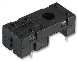
## Socket
## **TYPES**
|**TYPES**|||||||||
|---|---|---|---|---|---|---|---|---|
|Product name|Number of<br>poles|Part No.|Applicable relay type||||Standard packing||
||||1 Form A|1 Form C|2 Form A|2 Form C|Inner carton|Outer case|
|JW1 DIN terminal socket<br>(with hold-down clip)|JW1 DIN terminal socket<br>1|JW1-SFD|•|•|||10 pcs.|100 pcs.|
|JW2 DIN terminal socket<br>(with hold-down clip)|JW2 DIN terminal socket<br>2|JW2-SFD|||•|•|||
|JW1 PC board socket|1|JW1-PS|•|•|||||
|JW2 PC board socket|2|JW2-PS|||•|•|||
|JW1 Plug-in socket|1|JW1-SS|•|•|||||
|JW2 Plug-in socket|2|JW2-SS|||•|•|||
|**SPECIFICATIONS**|||||||||
|Type<br>Item|Type<br>PC board socket/Plug-in socket<br>1 pole<br>2 poles||||DIN terminal socket||||
||||2 poles||1 pole||2 poles||
|Breakdown voltage|1,500 vrms for 1 minute||||1,500 Vrms for 1 minute||1,000 Vrms for 1 minute||
|Insulation resistance|Min. 100 MΩ||||Min. 100 MΩ||||
## **SPECIFICATIONS**
|**SPECIFICATIONS**|||||
|---|---|---|---|---|
|Type|Type|PC board socket/Plug-in socket||DIN terminal socket|
|Item||1 pole|2 poles|1 pole<br>2 poles|
|Breakdown voltage||1,500 vrms for 1 minute||1,500 Vrms for 1 minute<br>1,000 Vrms for 1 minute|
|Insulation resistance||Min. 100 MΩ||Min. 100 MΩ|
## **DIMENSIONS**
**==> picture [528 x 197] intentionally omitted <==**
**----- Start of picture text -----**<br>
DIMENSIONS mm inch<br>1. DIN terminal socket 2. PC board socket PC board pattern (Bottom view)<br>1 Form A<br>20.6±0.6 0.8±0.1<br>7.5±0.2 .811±.024 .031±.004 1 Form C<br>.295±.008<br>aun a 13±0.6 fae sa = 5-1.3 dia.<br>.512±.024 5-.051 dia.<br> 5±0.3 67±1<br>.197±.012 2.638±.039 32±0.6<br>1.260±.024 7.6<br>6.5 dia. .299<br>.256 dia. 6.5 35.4±0.5<br>.256 1.394±.020 (4.4) 16.5 3.5<br>.197 5±±.0120.3 .591 15±±0.3.012 21.5±0.6 (.173) .650 .1383.5 .138<br>.1694.3±.012±0.3 3.5 dia. .1383.5 .846±.024 2 Form A<br>.138 dia. 6.7±0.3 2 Form C<br>.264±.012 0.3±0.1<br> 4±0.6 .012±.004 8-1.3 dia.<br>.157±.024 8-.051 dia.<br>peer" L| Pre-soldering .0140.35±±.0040.1 ee<br>.82721±±0.6 .024 7.5.295<br> 3±0.3 28.5±0.6 [e999<br>.118±.012 1.122±.024<br>(4) JE 15 TITEL 5 5 |<br>(.157) .591 .197 .197<br>Tolerance: ±0.1 ±.004<br>1 8<br>3 6<br>4 5<br>2 7<br>**----- End of picture text -----**<br>
## 1. DIN terminal socket
**==> picture [347 x 149] intentionally omitted <==**
**----- Start of picture text -----**<br>
3. Plug-in socket<br>Panel cut-out<br>.512 13±±.0240.6 * @]a-—o og a. (Thickness: 1.0 to 2.0 .039 to .079)<br>|<br> 37±0.6 34.9<br>1.457±.024 1.374<br> 1±0.3<br>36.4±0.6 .039±.012 11.9<br>1.433±.024 .469<br> 2±0.3<br> 25.4±0.6 .079±.012 Tolerance: ±0.1 ±.004<br>1.000±.024<br> 2±0.3<br>.079±.012<br> 8.6±0.3<br>.339±.012<br>.315 8±±.0240.6 Yo) Bee .0751.9 I ±±0.3.012<br>Details of<br>terminal portion<br>**----- End of picture text -----**<br>
## **For Cautions for Use, see Relay Technical Information.**
All Rights Reserved © COPYRIGHT Matsushita Electric Works, Ltd.
Updated at February 9, 2023
Panasonic Industry is a global leader in the design and manufacture of high-quality electronic components. Renowned for a commitment to continuous innovation, the company provides the essential building blocks that empower modern engineering. From industrial automation to consumer electronics, Panasonic's components are trusted worldwide for their outstanding reliability, efficiency, and long-term performance. The extensive portfolio is anchored by a massive selection of passive components, featuring an industry-leading range of aluminium electrolytic, film, and polymer capacitors. Alongside these advanced capacitance solutions, engineers rely on Panasonic's robust power inductors and a highly versatile array of electromechanical devices, including solid-state, power, and signal relays engineered to excel in demanding environments. Beyond core passives and switching solutions, the offering encompasses critical circuit protection devices such as TVS varistors and NTC thermistors, as well as sophisticated thermal management materials. Panasonic also delivers precision light and motion sensors, highly reliable batteries, and advanced Bluetooth and WLAN connectivity modules, providing a comprehensive ecosystem of components to support next-generation technological design.
About Novapart
Novapart is a B2B electronic component broker specialising in stock shortages and cost reduction. We source hard-to-find parts and identify compliant alternatives across a catalogue of 410,000+ components from 500+ manufacturers.
Learn more →Stock Shortage Specialist
When a component is unavailable, discontinued or has an unacceptable lead time, we tap into our network of vetted European and Asian distributors to source what you need — without compromising on quality or traceability.
Request a quote →Compliant Alternatives
We identify pin-to-pin, electrically equivalent substitutes that meet the same certifications (RoHS, AEC-Q100, REACH) as your original specification — validated against datasheets, not just part numbers. Often at a lower cost.
BOM Analysis service →