


J176-D74Z
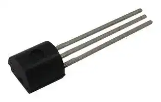
JFET Transistor, JFET, 30 V, -25 mA, 4 V, TO-92, 3 Pin, 150 °C
- Manufacturer: ONSEMI
- Product type: JFETs
- SVHC: No SVHC (25-Jun-2025)
- No. of Pins: 3 Pin
- Channel Type: P Channel
- Product Range: -
- Qualification: -
- Transistor Mounting: Through Hole
- Transistor Case Style: TO-92
- Operating Temperature Max: 150°C
- Gate Source Cutoff Voltage Max: 4V
- Gate Source Breakdown Voltage Max: 30V
- Zero Gate Voltage Drain Current Max: -25mA
| Delivery and price | |
|---|---|
| Units per pack | 6000 |
| Price | 0.102 € |
| Current stock | 10+ |
| Lead time | 30 days |
## **Is Now Part of**

## **To learn more about ON Semiconductor, please visit our website at www.onsemi.com**

Please note: As part of the Fairchild Semiconductor integration, some of the Fairchild orderable part numbers will need to change in order to meet ON Semiconductor’s system requirements. Since the ON Semiconductor product management systems do not have the ability to manage part nomenclature that utilizes an underscore (_), the underscore (_) in the Fairchild part numbers will be changed to a dash (-). This document may contain device numbers with an underscore (_). Please check the ON Semiconductor website to verify the updated device numbers. The most current and up-to-date ordering information can be found at www.onsemi.com. Please email any questions regarding the system integration to Fairchild_questions@onsemi.com.

ON Semiconductor and the ON Semiconductor logo are trademarks of Semiconductor Components Industries, LLC dba ON Semiconductor or its subsidiaries in the United States and/or other countries. ON Semiconductor owns the rights to a number of patents, trademarks, copyrights, trade secrets, and other intellectual property. A listing of ON Semiconductor’s product/patent coverage may be accessed at www.onsemi.com/site/pdf/Patent-Marking.pdf. ON Semiconductor reserves the right to make changes without further notice to any products herein. ON Semiconductor makes no warranty, representation or guarantee regarding the suitability of its products for any particular purpose, nor does ON Semiconductor assume any liability arising out of the application or use of any product or circuit, and specifically disclaims any and all liability, including without limitation special, consequential or incidental damages. Buyer is responsible for its products and applications using ON Semiconductor products, including compliance with all laws, regulations and safety requirements or standards, regardless of any support or applications information provided by ON Semiconductor. “Typical” parameters which may be provided in ON Semiconductor data sheets and/or specifications can and do vary in different applications and actual performance may vary over time. All operating parameters, including “Typicals” must be validated for each customer application by customer’s technical experts. ON Semiconductor does not convey any license under its patent rights nor the rights of others. ON Semiconductor products are not designed, intended, or authorized for use as a critical component in life support systems or any FDA Class 3 medical devices or medical devices with a same or similar classification in a foreign jurisdiction or any devices intended for implantation in the human body. Should Buyer purchase or use ON Semiconductor products for any such unintended or unauthorized application, Buyer shall indemnify and hold ON Semiconductor and its officers, employees, subsidiaries, affiliates, and distributors harmless against all claims, costs, damages, and expenses, and reasonable attorney fees arising out of, directly or indirectly, any claim of personal injury or death associated with such unintended or unauthorized use, even if such claim alleges that ON Semiconductor was negligent regarding the design or manufacture of the part. ON Semiconductor is an Equal Opportunity/Affirmative Action Employer. This literature is subject to all applicable copyright laws and is not for resale in any manner.

**==> picture [68 x 10] intentionally omitted <==**

**----- Start of picture text -----**<br>
September 2015<br>**----- End of picture text -----**<br>


## **J175 / J176 / MMBFJ175 / MMBFJ176 / MMBFJ177 P-Channel Switch**

## **Description**

This device is designed for low-level analog switching sample-and-hold circuits and chopper-stabilized amplifiers. Sourced from process 88.

**G TO-92** 1. Drain **S** 2. Gate **SOT-23 D** 1 2 3 @ 1 2 3. Source **Mark: 6W / 6X / 6Y** 3 **Note: Source & drain are interchangeable. Straight Lead        Bent Lead Bulk Packing       Tape & Reel Ammo Packing**

**Figure 1. J175 / J176 Device Package**

**Figure 2. MMBFJ175 / 176 / 177 Device Package**

**Ordering Information**

**Part Number Marking Package Packing Method** J175_D26Z J175 TO-92 3L Tape and Reel J176_D74Z J176 TO-92 3L Ammo MMBFJ175 6W SOT-23 3L Tape and Reel MMBFJ176 6X SOT-23 3L Tape and Reel MMBFJ177 6Y SOT-23 3L Tape and Reel ~~====~~

©1997 Fairchild Semiconductor Corporation J175 / J176 / MMBFJ175 / MMBFJ176 / MMBFJ177 Rev. 1.6

www.fairchildsemi.com

## **Absolute Maximum Ratings**[(1),(2)]

Stresses exceeding the absolute maximum ratings may damage the device. The device may not function or be operable above the recommended operating conditions and stressing the parts to these levels is not recommended. In addition, extended exposure to stresses above the recommended operating conditions may affect device reliability. The absolute maximum ratings are stress ratings only. Values are at TA = 25°C unless otherwise noted.

**Symbol Parameter Value Unit** VDG Drain-Gate Voltage -30 V VGS Gate-Source Voltage 30 V IGF Forward Gate Current 50 mA TJ, TSTG Operating and Storage Junction Temperature Range -55 to + 150 ° C ~~<=:~~ **Notes:**

1. These ratings are based on a maximum junction temperature of 150 ° C.

2. These are steady-state limits. Fairchild Semiconductor should be consulted on applications involving pulsed or low-duty cycle operations.

**Thermal Characteristics** Values are at TA = 25°C unless otherwise noted. **Max. Symbol Parameter MMBFJ175 / Unit J175 / J176**[(3)] **MMBFJ176 / MMBFJ177**[(3)] Total Device Dissipation 350 225 mW PD Derate Above 25 ° C 2.8 1.8 mW/ ° C R θ JC Thermal Resistance, Junction to Case 125 ° C/W R θ JA Thermal Resistance, Junction to Ambient 357 556 ° C/W ~~———~~ **Note:** 3. PCB size: FR-4, 76 mm x 114 mm x 1.57 mm (3.0 inch x 4.5 inch x 0.062 inch) with minimum land pattern size.

© 1997 Fairchild Semiconductor Corporation J175 / J176 / MMBFJ175 / MMBFJ176 / MMBFJ177 Rev. 1.6

www.fairchildsemi.com

2

## **Electrical Characteristics**

Values are at TA = 25°C unless otherwise noted.

|Values are at TA = 25°C unless otherwise noted.|Values are at TA = 25°C unless otherwise noted.A = 25°C unless otherwise noted.= 25°C unless otherwise noted.||||||
|---|---|---|---|---|---|---|
|**Symbol**|**Parameter**|**Conditions**||**Min.**|**Max.**|**Unit**|
|**Off Characteristics**|||||||
|V(BR)GSS|Gate-Source Breakdown Voltage|IG= 1.0μA, VDS= 0||30||V|
|IGSS|Gate Reverse Current|VGS= 20 V, VDS= 0|||1.0|nA|
|VGS(off)|Gate-Source Cut-Off Voltage|VDS= -15 V, ID= -10 nA|**J175 /**<br>**MMBFJ175**|3.0|6.0|V|
||||**J176 /**<br>**MMBFJ176**|1.0|4.0||
||||**MMBFJ177**|0.8|2.5||
|**On Characteristics**|||||||
|IDSS|Zero-Gate Voltage Drain Current(4)|VDS= -15 V, IGS= 0|**J175 /**<br>**MMBFJ175**|-7.0|-60.0|mA|
||||**J176 /**<br>**MMBFJ176**|-2.0|-25.0||
||||**MMBFJ177**|-1.5|-20.0||
|rDS(on)|Drain-Source On Resistance|VDS ≤ 0.1 V, VGS= 0|**J175 /**<br>**MMBFJ175**||125|Ω|
||||**J176 /**<br>**MMBFJ176**||250||
||||**MMBFJ177**||300||


## **Note:**

4. Pulse test: pulse width ≤ 300 μ s, duty cycle ≤ 2.0%.

© 1997 Fairchild Semiconductor Corporation J175 / J176 / MMBFJ175 / MMBFJ176 / MMBFJ177 Rev. 1.6

www.fairchildsemi.com

3

## **Typical Performance Characteristics**

**==> picture [438 x 529] intentionally omitted <==**

**----- Start of picture text -----**<br>
-20 100 1,000<br>T    A = 25°C<br>TYP   V            = 4.5 VGS(off) EF 50 SSS =a 500<br>-16 0.5 V I DSS<br>-12 Te V      = 0 VGS 1.0 V pr r DS g fs<br>Ze pow ef<br>Aa 10 i seas 100<br>1.5 V<br>-8<br>a 7e—.e8nm 2.0 V 5 SS Seaee 50<br>I        DSS , g fs @ V     = 15VDS ,<br>-4 2.5 V 3.0 V 3.5 V V     = 0 PULSED r     @ -100 mV, V     = 0DS GS GS<br>Zee ee V           @ V      = - 15V,GS(off) DS<br>I     = - 1.0 D μ A<br>0 ) ae 1 pT I 10<br>0 -1 -2 -3 -4 -5 1 2 5 10<br>V    - DRAIN-SOURCE VOLTAGE (V)DS V             - GATE CUTOFF VOLTAGE (V)GS (OFF)<br>Figure 3. Common Drain-Source Figure 4. Parameter Interactions<br>-32 16<br>V      = - 15 VDS V      = - 15 VDS<br>V            = - 4.5 VGS(off) V            = - 4.5 V GS(off)- 55°C<br>-24 AL - 55°C PT 12 aN 25°C =<br>25°C 125°C<br>-16 SS 125°C V            = 2.5 VGS(off)- 55°C i 8 NSS V            = 2.5 VGS(off) - 55°C<br>25 ° C 25°C<br>125°C<br>125°C<br>-8 4<br>0 0<br>0 1 2 3 4 0 1 2 3 4<br>V    - GATE-SOURCE VOLTAGE (V)GS V    - GATE-SOURCE VOLTAGE (V)GS<br>Figure 5. Transfer Characteristics Figure 6. Transfer Characteristics<br>100 1000<br>V             @ 5.0V, 10 GS(off) μ A f = 1.0 kHz<br>50<br>-5.0V -5.0V<br>20 r     = DS 1  -   ________V r GSDS oe a 100 el -10V -20V -10V<br>10 — V GS(off) ———_———— V             = - 4.5VGS(off) —— -20V Tf ty<br>5 |} 4 10 ed<br>V             GS(off) = - 2.5V<br>2 pit+T [i een<br>1 0 0.2 0.4 0.6 0.8 1 _ 10.01 _ 0.1 oi _ 1 ooh _ 10<br>V    /V         - NORMALIZED GATE-SOURCE VOLTAGE (V)GS GS(off) I    - DRAIN CURRENT (mA)D<br>DS<br>D<br>I     - DRAIN CURRENT (mA)<br>fs (r      - DRAIN "ON" RESISTANCE<br>g     - TRANSCONDUCTANCE (mmhos) ) Ω<br>D D<br>I     - DRAIN CURRENT (mA) I     - DRAIN CURRENT (mA)<br>(  Ω )<br>μ<br>DS<br>r      - NORMALIZED RESISTANCE<br>os<br>g      - OUTPUT CONDUCTANCE (   mhos)<br>**----- End of picture text -----**<br>


**Figure 7. Normalized Drain Resistance vs. Bias Voltage**

**Figure 8. Output Conductance vs. Drain Current**

© 1997 Fairchild Semiconductor Corporation J175 / J176 / MMBFJ175 / MMBFJ176 / MMBFJ177 Rev. 1.6

www.fairchildsemi.com

4

## **Typical Performance Characteristics** (Continued)

**==> picture [428 x 148] intentionally omitted <==**

**----- Start of picture text -----**<br>
100<br>10 es Se ee  ——— f  = 0.1 - 1.0 MHz<br>V             = 2.5V GS(off) =——SSe Senet Se<br>5 25°C<br>||neeCee ORT a<br>V             = 6.0V GS(off)<br>- 55°C<br>1 25°C 10 C      is (V      = -15VDS )<br>PP 224ii\| RAN 125°C SERRE<br>0.5 oon oon 5 SS + C      (V       rs DS = -15V) t-—<br>V      = -15VDG a [TF _<br>f = 1.0 kHz<br>Ico Co FARRER<br>0.1<br>_ 0.1 _ 1 _ 10 _ 100 1<br>0 4 8 12 16 20<br>I    - DRAIN CURRENT (mA)D<br>V      - GATE-SOURCE VOLTAGE (V)GS<br>rs<br>is<br>C     (C      ) - CAPACITANCE (pF)<br>fs<br>g     - TRANSCONDUCTANCE (mmhos)<br>**----- End of picture text -----**<br>


**Figure 9. Transconductance vs. Drain Current**

**Figure 10. Capacitance vs. Voltage**

**==> picture [425 x 323] intentionally omitted <==**

**----- Start of picture text -----**<br>
100<br>1000<br>50 EE — V      = -100 mVDS<br>I     = - 0.2 mAD 500 V             = 2.5V GS(off) V      = 0GS<br>SN a x Z V             = 4.5V GS(off) =<br>Se Saini lil V             = 8.0V GS(off) ===<br>10 I     = 5.0 mAD ATSSP 100 pp SESS<br>5 | V       DG = - 15V DE | 50 aes ee a<br>BW = 6.0 Hz @ f = 10 Hz, 100 Hz<br>       = 0.2f @ f  ≥  1.0 kHz<br>1 10<br>0.01 0.1 1 10 100 -50 0 50 100 150<br>f - FREQUENCY (kHz) T     - AMBIENT TEMPERATURE (  C)A o<br>Figure 11. Noise Voltage vs. Frequency Figure 12. Channel Resistance vs. Temperature<br>350 Po ING<br>300 ee NS ee ee ee eee<br>TO-92<br>250<br>PEN fb<br>200 aee eeeeee ee<br>150 ee ee ee NG ee ee<br>SOT-23<br>100 |Pf ee IRSe Ne ee<br>oN ee<br>50<br>0<br>0 25 50 75 100 125 150<br>TEMPERATURE  (  C)o<br>D<br>)( Ω<br>√<br>e    - NOISE VOLTAGE (nV /   Hz)n DS<br>r     - DRAIN "ON" RESISTANCE<br>P   - POWER DISSIPATION (mW)<br>**----- End of picture text -----**<br>


**Figure 12. Channel Resistance vs. Temperature**

**Figure 13. Power Dissipation vs. Ambient Temperature**

© 1997 Fairchild Semiconductor Corporation J175 / J176 / MMBFJ175 / MMBFJ176 / MMBFJ177 Rev. 1.6

www.fairchildsemi.com

5

## **Physical Dimensions**

**Figure 14. 3-Lead, TO-92, Molded, 0.2 In Line Spacing Lead Form**

© 1997 Fairchild Semiconductor Corporation J175 / J176 / MMBFJ175 / MMBFJ176 / MMBFJ177 Rev. 1.6

www.fairchildsemi.com

6

**==> picture [420 x 526] intentionally omitted <==**

**----- Start of picture text -----**<br>
Physical Dimensions  (Continued)<br>0.95<br>2.92±0.20<br>3<br>1.40<br>1.30 [+0.20] 2.20<br>-0.15<br>— fe a |<br>1 2<br>(0.29) 0.60<br>0.37<br>0.95<br>0.20 A B 1.00<br>He? 1.90 1.90<br>LAND PATTERN<br>RECOMMENDATION<br>1.20 MAX SEE DETAIL A<br>(0.93) 0.10<br>0.00<br>0.10 C<br>C<br>2.40±0.30<br>NOTES: UNLESS OTHERWISE SPECIFIED<br>GAGE PLANE<br>   A)  REFERENCE JEDEC REGISTRATION<br>TO-236, VARIATION AB, ISSUE H.<br>0.23    B)  ALL DIMENSIONS ARE IN MILLIMETERS.<br>0.08    C)  DIMENSIONS ARE INCLUSIVE OF BURRS,<br>0.25        MOLD FLASH AND TIE BAR EXTRUSIONS.<br>   D)  DIMENSIONING AND TOLERANCING PER<br>       ASME Y14.5M - 1994.<br>0.20 MIN SEATING    E)  DRAWING FILE NAME: MA03DREV10<br>m i (0.55) es PLANE<br>SCALE: 2X<br>**----- End of picture text -----**<br>


**Figure 15. 3-LEAD, SOT23, JEDEC TO-236, LOW PROFILE**

© 1997 Fairchild Semiconductor Corporation J175 / J176 / MMBFJ175 / MMBFJ176 / MMBFJ177 Rev. 1.6

www.fairchildsemi.com

7

## **TRADEMARKS**

The following includes registered and unregistered trademarks and service marks, owned by Fairchild Semiconductor and/or its global subsidiaries, and is not intended to be an exhaustive list of all such trademarks.

AccuPower F-PFS OPTOPLANAR[®] AttitudeEngine™ ™ FRFET ™[®] fe GENERALSYSTEM ®* AX-CAPAwindaBitSiC ~~™~~[®][®] * Global Power ResourceGreenBridgeGreen FPS ~~™~~ ™ SM Power Supply WebDesignerPowerTrench®[®] ™ TinyBoostTinyBuckTinyCalc[®][®] Build it Now ~~™~~ Green FPS ™ e-Series ™ PowerXS™ TinyLogic[®] CorePLUS ~~™~~ G _max_ ~~™~~ Programmable Active Droop TINYOPTO CorePOWER ~~™~~ GTO ™ QFET[®] TinyPower ™ _CROSSVOLT_ ™ IntelliMAX ™ QS ™ TinyPWM ™ CTL ™ ISOPLANAR ™ Quiet Series TinyWire Current Transfer Logic ™ Making Small Speakers Sound Louder RapidConfigure ™ TranSiC ™ DEUXPEED[®] and Better™ TriFault Detect Dual Cool™ MegaBuck ™” TRUECURRENT[®] * EfficientMaxEcoSPARK[®] ™ MICROCOUPLERMicroFET ™ Saving our world, 1mW/W/kW at a time™ SignalWise ™ Lu SerDes ™ ESBC® ™ MicroPakMicroPak2 ™" SMART STARTSmartMax ™ ™M UHC Z[®] Des : ~~-~~ MillerDrive **™** Solutions for Your Success ™ Ultra FRFET FACT Quiet SeriesFACTFairchildFastvCoreFETBenchFairchild SemiconductorFPS ™[®][®] ~~™™~~ ™[®] MotionGridMTiMTxMVNmWSaverOptoHiTMotionMax[®][®][®] ™[®][®] ™ SuperFETSPMSTEALTHSuperSOTSuperSOTSuperSOTSupreMOS[®] ™™™[®] ™[®] -3 -6 -8 Xsens™UniFETVCXVisualMaxVoltagePlusXS™ (l=x=™ ® ™ ™ OPTOLOGIC[®] SyncFET Sync-Lock™

* Trademarks of System General Corporation, used under license by Fairchild Semiconductor.

## **DISCLAIMER**

FAIRCHILD SEMICONDUCTOR RESERVES THE RIGHT TO MAKE CHANGES WITHOUT FURTHER NOTICE TO ANY PRODUCTS HEREIN TO IMPROVE RELIABILITY, FUNCTION, OR DESIGN. TO OBTAIN THE LATEST, MOST UP-TO-DATE DATASHEET AND PRODUCT INFORMATION, VISIT OUR WEBSITE AT HTTP://WWW.FAIRCHILDSEMI.COM. FAIRCHILD DOES NOT ASSUME ANY LIABILITY ARISING OUT OF THE APPLICATION OR USE OF ANY PRODUCT OR CIRCUIT DESCRIBED HEREIN; NEITHER DOES IT CONVEY ANY LICENSE UNDER ITS PATENT RIGHTS, NOR THE RIGHTS OF OTHERS. THESE SPECIFICATIONS DO NOT EXPAND THE TERMS OF FAIRCHILD’S WORLDWIDE TERMS AND CONDITIONS, SPECIFICALLY THE WARRANTY THEREIN, WHICH COVERS THESE PRODUCTS.

## **AUTHORIZED USE**

Unless otherwise specified in this data sheet, this product is a standard commercial product and is not intended for use in applications that require extraordinary levels of quality and reliability. This product may not be used in the following applications, unless specifically approved in writing by a Fairchild officer: (1) automotive or other transportation, (2) military/aerospace, (3) any safety critical application – including life critical medical equipment – where the failure of the Fairchild product reasonably would be expected to result in personal injury, death or property damage. Customer’s use of this product is subject to agreement of this Authorized Use policy. In the event of an unauthorized use of Fairchild’s product, Fairchild accepts no liability in the event of product failure. In other respects, this product shall be subject to Fairchild’s Worldwide Terms and Conditions of Sale, unless a separate agreement has been signed by both Parties.

## **ANTI-COUNTERFEITING POLICY**

Fairchild Semiconductor Corporation's Anti-Counterfeiting Policy. Fairchild's Anti-Counterfeiting Policy is also stated on our external website, www.fairchildsemi.com, under Terms of Use

Counterfeiting of semiconductor parts is a growing problem in the industry. All manufacturers of semiconductor products are experiencing counterfeiting of their parts. Customers who inadvertently purchase counterfeit parts experience many problems such as loss of brand reputation, substandard performance, failed applications, and increased cost of production and manufacturing delays. Fairchild is taking strong measures to protect ourselves and our customers from the proliferation of counterfeit parts. Fairchild strongly encourages customers to purchase Fairchild parts either directly from Fairchild or from Authorized Fairchild Distributors who are listed by country on our web page cited above. Products customers buy either from Fairchild directly or from Authorized Fairchild Distributors are genuine parts, have full traceability, meet Fairchild's quality standards for handling and storage and provide access to Fairchild's full range of up-to-date technical and product information. Fairchild and our Authorized Distributors will stand behind all warranties and will appropriately address any warranty issues that may arise. Fairchild will not provide any warranty coverage or other assistance for parts bought from Unauthorized Sources. Fairchild is committed to combat this global problem and encourage our customers to do their part in stopping this practice by buying direct or from authorized distributors.

## **PRODUCT STATUS DEFINITIONS**

**Definition of Terms**

|**Datasheet Identification**|**Product Status**|**Definition**|
|---|---|---|
|Advance Information|Formative / In Design|Datasheet contains the design specifications for product development. Specifications may change<br>in anymanner without notice.|
|Preliminary|First Production|Datasheet contains preliminary data; supplementary data will be published at a later date. Fairchild<br>Semiconductor reserves the right to make changes at anytime without notice to improve design.|
|No Identification Needed|Full Production|Datasheet contains final specifications. Fairchild Semiconductor reserves the right to make<br>changes at anytime without notice to improve the design.|
|Obsolete|Not In Production|Datasheet contains specifications on a product that is discontinued by Fairchild Semiconductor.<br>The datasheet is for reference information only.|


Rev. I77

© Fairchild Semiconductor Corporation

www.fairchildsemi.com

ON Semiconductor and      are trademarks of Semiconductor Components Industries, LLC dba ON Semiconductor or its subsidiaries in the United States and/or other countries. ON Semiconductor owns the rights to a number of patents, trademarks, copyrights, trade secrets, and other intellectual property. A listing of ON Semiconductor’s product/patent coverage may be accessed at www.onsemi.com/site/pdf/Patent−Marking.pdf. ON Semiconductor reserves the right to make changes without further notice to any products herein. ON Semiconductor makes no warranty, representation or guarantee regarding the suitability of its products for any particular purpose, nor does ON Semiconductor assume any liability arising out of the application or use of any product or circuit, and specifically disclaims any and all liability, including without limitation special, consequential or incidental damages. Buyer is responsible for its products and applications using ON Semiconductor products, including compliance with all laws, regulations and safety requirements or standards, regardless of any support or applications information provided by ON Semiconductor. “Typical” parameters which may be provided in ON Semiconductor data sheets and/or specifications can and do vary in different applications and actual performance may vary over time. All operating parameters, including “Typicals” must be validated for each customer application by customer’s technical experts. ON Semiconductor does not convey any license under its patent rights nor the rights of others. ON Semiconductor products are not designed, intended, or authorized for use as a critical component in life support systems or any FDA Class 3 medical devices or medical devices with a same or similar classification in a foreign jurisdiction or any devices intended for implantation in the human body. Should Buyer purchase or use ON Semiconductor products for any such unintended or unauthorized application, Buyer shall indemnify and hold ON Semiconductor and its officers, employees, subsidiaries, affiliates, and distributors harmless against all claims, costs, damages, and expenses, and reasonable attorney fees arising out of, directly or indirectly, any claim of personal injury or death associated with such unintended or unauthorized use, even if such claim alleges that ON Semiconductor was negligent regarding the design or manufacture of the part. ON Semiconductor is an Equal Opportunity/Affirmative Action Employer. This literature is subject to all applicable copyright laws and is not for resale in any manner.

## **PUBLICATION ORDERING INFORMATION**

**N. American Technical Support** : 800−282−9855 Toll Free **ON Semiconductor Website** : **www.onsemi.com** USA/Canada

## **LITERATURE FULFILLMENT** :

Literature Distribution Center for ON Semiconductor

**Order Literature** : http://www.onsemi.com/orderlit For additional information, please contact your local Sales Representative

19521 E. 32nd Pkwy, Aurora, Colorado 80011 USA **Europe, Middle East and Africa Technical Support: Phone** : 303−675−2175 or 800−344−3860 Toll Free USA/Canada Phone: 421 33 790 2910 **Fax** : 303−675−2176 or 800−344−3867 Toll Free USA/Canada **Japan Customer Focus Center Email** : orderlit@onsemi.com Phone: 81−3−5817−1050

© Semiconductor Components Industries, LLC

www.onsemi.com

**www.onsemi.com**

**1**
Updated at April 29, 2026
onsemi is a premier global supplier of intelligent power and sensing technologies, driving disruptive innovations across the automotive, industrial, and cloud infrastructure markets. Recognized for their commitment to sustainability and reliable supply chains, the company accelerates advancements in vehicle electrification, industrial automation, and 5G networks by solving the industry's most complex design challenges. At the core of their portfolio is an industry-leading selection of discrete semiconductors. This extensive range features thousands of high-performance bipolar transistors, single and dual MOSFETs, and a comprehensive array of diodes, including Zener, Schottky, and fast-recovery rectifiers. Engineered for superior thermal performance and energy efficiency, these foundational components are critical for demanding power conversion, switching, and signal conditioning applications. Beyond essential discretes, onsemi provides a robust suite of advanced power management and circuit protection solutions. Their lineup includes intelligent power modules, single IGBTs, and transient voltage suppression (TVS) diodes designed to safeguard sensitive circuitry. Complimented by integrated passive filters, AC/DC LED driver ICs, and specialized sub-2.4GHz RF transceivers, onsemi equips engineers with the scalable, high-quality technologies needed to build a cleaner, smarter, and more connected world.
About Novapart
Novapart is a B2B electronic component broker specialising in stock shortages and cost reduction. We source hard-to-find parts and identify compliant alternatives across a catalogue of 420,000+ components from 500+ manufacturers.
Learn more →Stock Shortage Specialist
When a component is unavailable, discontinued or has an unacceptable lead time, we tap into our network of vetted European and Asian distributors to source what you need — without compromising on quality or traceability.
Request a quote →Compliant Alternatives
We identify pin-to-pin, electrically equivalent substitutes that meet the same certifications (RoHS, AEC-Q100, REACH) as your original specification — validated against datasheets, not just part numbers. Often at a lower cost.
BOM Analysis service →