
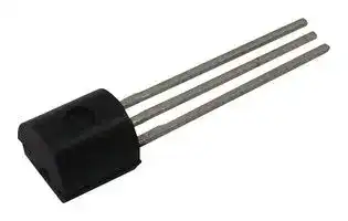


J112
JFET Transistor, -35 V, -5 V, TO-92, 3 Pin, 150 °C
- Manufacturer: ONSEMI
- Product type: JFETs
- Breakdown Voltage Vbr:-35V; Zero Gate Voltage Drain Current Idss Min:5mA; Zero Gate Voltage Drain Current Idss Max:-; Gate-Source Cutoff Voltage Vgs(off) Max:-5V; Transistor Case Style:TO-9
- MSL: MSL 1 - Unlimited
- SVHC: No SVHC (25-Jun-2025)
- No. of Pins: 3 Pin
- Channel Type: N Channel
- Product Range: -
- Qualification: -
- Transistor Type: JFET
- Transistor Mounting: Through Hole
- Transistor Case Style: TO-92
- Operating Temperature Max: 150°C
- Gate Source Cutoff Voltage Max: -5V
- Gate Source Breakdown Voltage Max: -35V
- Zero Gate Voltage Drain Current Max: -
- Zero Gate Voltage Drain Current Idss Min: 5mA
| Delivery and price | |
|---|---|
| Units per pack | 5000 |
| Price | 0.097 € |
| Current stock | 1000+ |
| Lead time | 30 days |
J111, J112

## JFET Chopper Transistors **N−Channel — Depletion**

## **Features**

- Pb−Free Packages are Available*

## **http://onsemi.com**

1 DRAIN **MAXIMUM RATINGS Rating Symbol Value Unit** 3 Drain−Gate Voltage VDG −35 Vdc GATE Gate−Source Voltage VGS −35 Vdc Gate Current IG 50 mAdc 2 SOURCE Total Device Dissipation @ TA = 25 ° C PD 350 mW Derate above = 25 ° C 2.8 mW/ ° C Lead Temperature TL 300 ° C Operating and Storage Junction TJ, Tstg −65 to +150 ° C Temperature Range Maximum ratings are those values beyond which device damage can occur. Maximum ratings applied to the device are individual stress limit values (not **TO−92** normal operating conditions) and are not valid simultaneously. If these limits are 1 **CASE 29−11** exceeded, device functional operation is not implied, damage may occur and ~~oe,~~ 2 3 **STYLE 5** reliability may be affected. **MARKING DIAGRAM**

**==> picture [26 x 16] intentionally omitted <==**

**----- Start of picture text -----**<br>
J11x<br>AYWW<br>**----- End of picture text -----**<br>


J11x = Device Code x = 1 or 2 A = Assembly Location Y = Year WW = Work Week = Pb−Free Package

(Note: Microdot may be in either location)

## **ORDERING INFORMATION**

See detailed ordering and shipping information in the package dimensions section on page 2 of this data sheet.

*For additional information on our Pb−Free strategy and soldering details, please download the ON Semiconductor Soldering and Mounting Techniques Reference Manual, SOLDERRM/D.

Publication Order Number: **J111/D**

**1**

© Semiconductor Components Industries, LLC, 2006 **March, 2006 − Rev. 2**

**J111, J112**

## **ELECTRICAL CHARACTERISTICS** (TA = 25 ° C unless otherwise noted)

|**ELECTRICAL CHARACTERISTICS**(TA= 25°C unless otherwise noted)|||||
|---|---|---|---|---|
|**Characteristic**|**Symbol**|**Min**|**Max**|**Unit**|
|**OFF CHARACTERISTICS**|||||
|Gate−Source Breakdown Voltage<br>(IG= −1.0�Adc)|V(BR)GSS|35|−|Vdc|
|Gate Reverse Current<br>(VGS= −15 Vdc)|IGSS|−|−1.0|nAdc|
|Gate Source Cutoff Voltage<br>(VDS= 5.0 Vdc, ID= 1.0�Adc)<br>J111<br>J112|VGS(off)|−3.0<br>−1.0|−10<br>−5.0|Vdc|
|Drain−Cutoff Current<br>(VDS= 5.0 Vdc, VGS= −10 Vdc)|ID(off)|−|1.0|nAdc|
|**ON CHARACTERISTICS**|||||
|Zero−Gate−Voltage Drain Current(1)<br>(VDS= 15 Vdc)<br>J111<br>J112|IDSS|20<br>5.0<br>2.0|−<br>−<br>−|mAdc|
|Static Drain−Source On Resistance<br>(VDS= 0.1 Vdc)<br>J111<br>J112|rDS(on)|−<br>−|30<br>50|�|
|Drain Gate and Source Gate On−Capacitance<br>(VDS= VGS= 0, f = 1.0 MHz)|Cdg(on)<br>+<br>Csg(on)|−|28|pF|
|Drain Gate Off−Capacitance<br>(VGS= −10 Vdc, f = 1.0 MHz)|Cdg(off)|−|5.0|pF|
|Source Gate Off−Capacitance<br>(VGS= −10 Vdc, f = 1.0 MHz)|Csg(off)|−|5.0|pF|


1. Pulse Width = 300 � s, Duty Cycle = 3.0%.

## **ORDERING INFORMATION**

|**ORDERING INFORMATION**|||
|---|---|---|
|**Device**|**Package**|**Shipping**†|
|J111RL1|TO−92|2000 Units / Tape & Reel|
|J111RL1G|TO−92<br>(Pb−Free)||
|J111RLRA|TO−92|2000 Units / Tape & Reel|
|J111RLRAG|TO−92<br>(Pb−Free)||
|J111RLRP|TO−92|2000 Units / Tape & Reel|
|J111RLRPG|TO−92<br>(Pb−Free)||
|J112|TO−92|1000 Units / Bulk|
|J112G|TO−92<br>(Pb−Free)||
|J112RL1|TO−92|2000 Units / Tape & Reel|
|J112RL1G|TO−92<br>(Pb−Free)||
|J112RLRA|TO−92|2000 Units / Tape & Reel|
|J112RLRAG|TO−92<br>(Pb−Free)||


†For information on tape and reel specifications, including part orientation and tape sizes, please refer to our Tape and Reel Packaging Specifications Brochure, BRD8011/D.

**http://onsemi.com**

**2**

**J111, J112**

## **TYPICAL SWITCHING CHARACTERISTICS**

**==> picture [235 x 370] intentionally omitted <==**

**----- Start of picture text -----**<br>
1000<br>500 TJ = 25°C<br>200 RK = RD′ J111 VGS(off) = 12 V<br>J112 = 7.0 V<br>100 J113 = 5.0 V<br>50<br>20<br>10<br>5.0 RK = 0<br>2.0<br>1.0<br>0.5 0.7 1.0 2.0 3.0 5.0 7.0 10 20 30 50<br>ID, DRAIN CURRENT (mA)<br>Figure 1. Turn−On Delay Time<br>1000 TJ = 25°C<br>500<br>J111 VGS(off) = 12 V<br>200 J112 = 7.0 V<br>J113 = 5.0 V<br>100<br>50 RK = RD′<br>20<br>10<br>5.0 RK = 0<br>2.0<br>1.0<br>0.5 0.7 1.0 2.0 3.0 5.0 7.0 10 20 30 50<br>ID, DRAIN CURRENT (mA)<br>td(on), TURN−ON DELAY TIME (ns)<br>td(off), TURN−OFF DELAY TIME (ns)<br>**----- End of picture text -----**<br>


**Figure 3. Turn−Off Delay Time**

**==> picture [236 x 370] intentionally omitted <==**

**----- Start of picture text -----**<br>
1000 TJ = 25°C<br>500<br>RK = RD′ J111 VGS(off) = 12 V<br>J112 = 7.0 V<br>200<br>J113 = 5.0 V<br>100<br>50<br>20<br>10 RK = 0<br>5.0<br>2.0<br>1.0<br>0.5 0.7 1.0 2.0 3.0 5.0 7.0 10 20 30 50<br>ID, DRAIN CURRENT (mA)<br>Figure 2. Rise Time<br>1000 TJ = 25°C<br>500 RK = RD′ J111 VGS(off) = 12 V<br>200 J112 = 7.0 V<br>J113 = 5.0 V<br>100<br>50<br>20<br>RK = 0<br>10<br>5.0<br>2.0<br>1.0<br>0.5 0.7 1.0 2.0 3.0 5.0 7.0 10 20 30 50<br>ID, DRAIN CURRENT (mA)<br>tr, RISE TIME (ns)<br>tf , FALL TIME (ns)<br>**----- End of picture text -----**<br>


**Figure 4. Fall Time**

## **NOTE 1**

**==> picture [225 x 173] intentionally omitted <==**

**----- Start of picture text -----**<br>
+VDD<br>RD<br>SET VDS(off) = 10 V<br>INPUT<br>RK RT<br>RGEN OUTPUT<br>50 � RGG<br>50 � 50 �<br>VGEN VGG<br>INPUT PULSE RGG � RK<br>tr ≤ 0.25 ns<br>PULSE WIDTHtf ≤= 2.0  0.5 ns�s RD�� RDRD(RT � RT � �50)50<br>DUTY CYCLE ≤ 2.0%<br>**----- End of picture text -----**<br>


**Figure 5.  Switching Time Test Circuit**

The switching characteristics shown above were measured using a test circuit similar to Figure 5. At the beginning of the switching interval, the gate voltage is at Gate Supply Voltage (−VGG). The Drain−Source Voltage (VDS) is slightly lower than Drain Supply Voltage (VDD) due to the voltage divider. Thus Reverse Transfer Capacitance (Crss) or Gate−Drain Capacitance (Cgd) is charged to VGG + VDS.

During the turn−on interval, Gate−Source Capacitance (Cgs) discharges through the series combination of RGen and RK. Cgd must discharge to VDS(on) through RG and RK in series with the parallel ′ combination of effective load impedance (R D) and Drain−Source Resistance (rds). During the turn−off, this charge flow is reversed.

Predicting turn−on time is somewhat difficult as the channel resistance rds is a function of the gate−source voltage. While Cgs discharges, VGS approaches zero and rds decreases. Since Cgd discharges through rds, turn−on time is non−linear. During turn−off, the situation is reversed with rds increasing as Cgd charges.

The above switching curves show two impedance conditions; 1) RK is equal to RD, which simulates the switching behavior of cascaded stages where the driving source impedance is normally the load impedance of the previous stage, and 2) RK = 0 (low impedance) the driving source impedance is that of the generator.

**http://onsemi.com**

**3**

**J111, J112**

**==> picture [488 x 607] intentionally omitted <==**

**----- Start of picture text -----**<br>
20 15<br>J112<br>10<br>J111 Cgs<br>10<br>J113 7.0<br>7.0 5.0 Cgd<br>5.0 Tchannel = 25°C<br>VDS = 15 V 3.0 Tchannel = 25°C<br>2.0 (Cds IS NEGLIGIBLE)<br>3.0<br>1.5<br>2.0 1.0<br>0.5 0.7 1.0 2.0 3.0 5.0 7.0 10 20 30 50 0.03 0.05 0.1 0.3 0.5 1.0 3.0 5.0 10 30<br>ID, DRAIN CURRENT (mA) VR, REVERSE VOLTAGE (VOLTS)<br>Figure 6. Typical Forward Transfer Admittance Figure 7. Typical Capacitance<br>200 2.0<br>= 10IDSS mA25 50�mA 75�mA 100�mA 125�mA 1.8 ID = 1.0 mA<br>mA VGS = 0<br>160<br>1.6<br>1.4<br>120<br>1.2<br>80 1.0<br>40 Tchannel = 25°C 0.8<br>0.6<br>0 0.4<br>0 1.0 2.0 3.0 4.0 5.0 6.0 7.0 8.0 −�70 −�40 −�10 20 50 80 110 140 170<br>VGS, GATE−SOURCE VOLTAGE (VOLTS) Tchannel, CHANNEL TEMPERATURE (°C)<br>Figure 8. Effect of Gate−Source Voltage Figure 9. Effect of Temperature On<br>On Drain−Source Resistance Drain−Source On−State Resistance<br>NOTE 2<br>100 Tchannel = 25°C 10 The Zero−Gate−Voltage Drain Current (IDSS), is the<br>90 9.0 principle determinant of other J-FET characteristics.<br>80 8.0 Figure 10 shows the relationship of Gate−Source Off<br>Voltage (VGS(off) and Drain−Source On Resistance<br>70 rDS(on) @ VGS = 0 7.0 (rds(on)) to IDSS. Most of the devices will be within ±10%<br>60 6.0 of the values shown in Figure 10. This data will be useful<br>50 VGS(off) 5.0 in predicting the characteristic variations for a given part<br>number.<br>40 4.0<br>For example:<br>30 3.0<br>Unknown<br>20 2.0 rds(on) and VGS range for an J112<br>10 1.0 The electrical characteristics table indicates that an J112<br>0 0 has an IDSS range of 25 to 75 mA. Figure 10, showsDSS range of 25 to 75 mA. Figure 10, shows range of 25 to 75 mA. Figure 10, shows<br>10 20 30 40 50 60 70 80 90 100 110 120 130 140 150 rds(on) = 52 ds(on) = 52 = 52  � for IDSS = 25 mA and 30  for IDSS = 25 mA and 30 DSS = 25 mA and 30  = 25 mA and 30  � for for<br>IDSS, ZERO−GATE−VOLTAGE DRAIN CURRENT (mA) IDSS = 75 mA. The corresponding VGS values are 2.2 VDSS = 75 mA. The corresponding VGS values are 2.2 V = 75 mA. The corresponding VGS values are 2.2 VGS values are 2.2 V values are 2.2 V<br>C, CAPACITANCE (pF)<br>yfs, FORWARD TRANSFER ADMITTANCE (mmho<br>RESISTANCE (OHMS)<br>RESISTANCE (NORMALIZED)<br>rds(on), DRAIN−SOURCE ON−STATE rds(on), DRAIN−SOURCE ON−STATE<br>RESISTANCE (OHMS)<br>rds(on), DRAIN−SOURCE ON−STATE<br>VGS, GATE−SOURCE VOLTAGE (VOLTS)<br>**----- End of picture text -----**<br>


The electrical characteristics table indicates that an J112 has an IDSS range of 25 to 75 mA. Figure 10, showsDSS range of 25 to 75 mA. Figure 10, shows range of 25 to 75 mA. Figure 10, shows rds(on) = 52 ds(on) = 52 = 52 � for IDSS = 25 mA and 30  for IDSS = 25 mA and 30 DSS = 25 mA and 30  = 25 mA and 30 � for for IDSS = 75 mA. The corresponding VGS values are 2.2 VDSS = 75 mA. The corresponding VGS values are 2.2 V = 75 mA. The corresponding VGS values are 2.2 VGS values are 2.2 V values are 2.2 V and 4.8 V.

**Figure 10. Effect of IDSS On Drain−Source Resistance and Gate−Source Voltage**

**http://onsemi.com**

**4**

MECHANICAL CASE OUTLINE **PACKAGE DIMENSIONS**

**==> picture [144 x 92] intentionally omitted <==**

**----- Start of picture text -----**<br>
SCALE 1:1<br>1<br>1 23 2 3<br>STRAIGHT LEAD BENT LEAD<br>BULK PACK TAPE & REEL<br>AMMO PACK<br>**----- End of picture text -----**<br>


**TO−92 (TO−226)** CASE 29−11 ISSUE AM

DATE 09 MAR 2007

**==> picture [214 x 182] intentionally omitted <==**

**----- Start of picture text -----**<br>
A B STRAIGHT LEAD<br>BULK PACK<br>R<br>P<br>L<br>SEATING<br>PLANE K<br>X X D<br>G<br>H J<br>V C<br>SECTION X−X<br>1 N<br>N<br>**----- End of picture text -----**<br>


## NOTES:

1. DIMENSIONING AND TOLERANCING PER ANSI Y14.5M, 1982.

2. CONTROLLING DIMENSION: INCH.

3. CONTOUR OF PACKAGE BEYOND DIMENSION R IS UNCONTROLLED.

4. LEAD DIMENSION IS UNCONTROLLED IN P AND

- BEYOND DIMENSION K MINIMUM.

|**DIM**|**INCHES**|**INCHES**|**MILLIMETERS**|**MILLIMETERS**|
|---|---|---|---|---|
||**MIN**|**MAX**|**MIN**|**MAX**|
|**A**|0.175|0.205|4.45|5.20|
|**B**|0.170|0.210|4.32|5.33|
|**C**|0.125|0.165|3.18|4.19|
|**D**<br>|0.016<br>|0.021<br>|0.407<br>|0.533<br>|
|**G**|0.045|0.055|1.15|1.39|
|**H**|0.095|0.105|2.42|2.66|
|**J**|0.015|0.020|0.39|0.50|
|**K**|0.500|---|12.70|---|
|**L**|0.250|---|6.35|---|
|**N**|0.080|0.105|2.04|2.66|
|**P**<br>|---<br>|0.100|---<br>|2.54|
|**R**<br>**V**|0.115<br>0.135|---<br>---|2.93<br>3.43|---<br>---|


**==> picture [207 x 181] intentionally omitted <==**

**----- Start of picture text -----**<br>
R A B BENT LEAD<br>TAPE & REEL<br>AMMO PACK<br>P<br>T<br>SEATINGPLANE K<br>X X D<br>G<br>J<br>V<br>C<br>SECTION X−X<br>1 N<br>**----- End of picture text -----**<br>


- NOTES: 1. DIMENSIONING AND TOLERANCING PER ASME Y14.5M, 1994.

2. CONTROLLING DIMENSION: MILLIMETERS.

3. CONTOUR OF PACKAGE BEYOND

- DIMENSION R IS UNCONTROLLED.

4. LEAD DIMENSION IS UNCONTROLLED IN P

- AND BEYOND DIMENSION K MINIMUM.

|**MILLIMETERS**|**MILLIMETERS**|
|---|---|
|**MIN**|**MAX**|
|4.45|5.20|
|4.32|5.33|
|3.18|4.19|
|0.40<br>|0.54<br>|
|2.40<br>0.39|2.80<br>0.50|
|1270|---|
|.<br>2.04|2.66|
|1.50|4.00|
|2.93|---|
|3.43|---|


## **STYLES ON PAGE 2**

**==> picture [491 x 72] intentionally omitted <==**

**----- Start of picture text -----**<br>
DOCUMENT NUMBER: 98ASB42022B Electronic versions are uncontrolled except when<br>accessed directly from the Document Repository. Printed<br>STATUS: ON SEMICONDUCTOR STANDARD<br>versions are uncontrolled except when stamped<br>“CONTROLLED COPY” in red.<br>NEW STANDARD:<br>©   Semiconductor Components Industries, LLC, 2002 http://onsemi.com Case Outline Number:<br>October, 2002 − Rev. 0DESCRIPTION: TO−92 (TO−226) 1 PAGE 1 OF 3XXX<br>**----- End of picture text -----**<br>


## **TO−92 (TO−226)** CASE 29−11 ISSUE AM

## DATE 09 MAR 2007

STYLE 1: STYLE 2: STYLE 3: PIN 1. EMITTER PIN 1. BASE PIN 1. ANODE 2. BASE 2. EMITTER 2. ANODE 3. COLLECTOR 3. COLLECTOR 3. CATHODE STYLE 6: STYLE 7: STYLE 8: PIN 1. GATE PIN 1. SOURCE PIN 1. DRAIN 2. SOURCE & SUBSTRATE 2. DRAIN 2. GATE 3. DRAIN 3. GATE 3. SOURCE & SUBSTRATE STYLE 11: STYLE 12: STYLE 13: PIN 1. ANODE PIN 1. MAIN TERMINAL 1 PIN 1. ANODE 1 2. CATHODE & ANODE 2. GATE 2. GATE 3. CATHODE 3. MAIN TERMINAL 2 3. CATHODE 2 STYLE 16: STYLE 17: STYLE 18: PIN 1. ANODE PIN 1. COLLECTOR PIN 1. ANODE 2. GATE 2. BASE 2. CATHODE 3. CATHODE 3. EMITTER 3. NOT CONNECTED STYLE 21: STYLE 22: STYLE 23: PIN 1. COLLECTOR PIN 1. SOURCE PIN 1. GATE 2. EMITTER 2. GATE 2. SOURCE 3. BASE 3. DRAIN 3. DRAIN STYLE 26: STYLE 27: STYLE 28: PIN 1. VCC PIN 1. MT PIN 1. CATHODE 2. GROUND 2 2. SUBSTRATE 2. ANODE 3. OUTPUT 3. MT 3. GATE STYLE 31: STYLE 32: STYLE 33: PIN 1. GATE PIN 1. BASE PIN 1. RETURN 2. DRAIN 2. COLLECTOR 2. INPUT 3. SOURCE 3. EMITTER 3. OUTPUT

STYLE 4: STYLE 5: PIN 1. CATHODE PIN 1. DRAIN 2. CATHODE 2. SOURCE 3. ANODE 3. GATE STYLE 9: STYLE 10: PIN 1. BASE 1 PIN 1. CATHODE 2. EMITTER 2. GATE 3. BASE 2 3. ANODE STYLE 14: STYLE 15: PIN 1. EMITTER PIN 1. ANODE 1 2. COLLECTOR 2. CATHODE 3. BASE 3. ANODE 2 STYLE 19: STYLE 20: PIN 1. GATE PIN 1. NOT CONNECTED 2. ANODE 2. CATHODE 3. CATHODE 3. ANODE STYLE 24: STYLE 25: PIN 1. EMITTER PIN 1. MT 1 2. COLLECTOR/ANODE 2. GATE 3. CATHODE 3. MT 2 STYLE 29: STYLE 30: PIN 1. NOT CONNECTED PIN 1. DRAIN 2. ANODE 2. GATE 3. CATHODE 3. SOURCE STYLE 34: STYLE 35: PIN 1. INPUT PIN 1. GATE 2. GROUND 2. COLLECTOR 3. LOGIC 3. EMITTER

**==> picture [491 x 72] intentionally omitted <==**

**----- Start of picture text -----**<br>
DOCUMENT NUMBER: 98ASB42022B Electronic versions are uncontrolled except when<br>accessed directly from the Document Repository. Printed<br>STATUS: ON SEMICONDUCTOR STANDARD<br>versions are uncontrolled except when stamped<br>“CONTROLLED COPY” in red.<br>NEW STANDARD:<br>©   Semiconductor Components Industries, LLC, 2002 http://onsemi.com Case Outline Number:<br>October, 2002 − Rev. 0DESCRIPTION: TO−92 (TO−226) 2 PAGE 2 OF 3XXX<br>**----- End of picture text -----**<br>


|~~eT ©~~|~~eT ©~~||**DOCUMENT NUMBER:**<br>**98ASB42022B**<br>**PAGE 3 OF 3**<br>~~——~~|
|---|---|---|---|
|**ISSUE**|**REVISION**||**DATE**|
|AM|ADDED BENT−LEAD TAPE & REEL VERSION. REQ. BY J. SUPINA.||09 MAR 2007|


> **ON Semiconductor** and          are registered trademarks of Semiconductor Components Industries, LLC (SCILLC).  SCILLC reserves the right to make changes without further notice to any products herein.  SCILLC makes no warranty, representation or guarantee regarding the suitability of its products for any particular purpose, nor does SCILLC assume any liability arising out of the application or use of any product or circuit, and specifically disclaims any and all liability, including without limitation special, consequential or incidental damages. “Typical” parameters which may be provided in SCILLC data sheets and/or specifications can and do vary in different applications and actual performance may vary over time.  All operating parameters, including “Typicals” must be validated for each customer application by customer’s technical experts.  SCILLC does not convey any license under its patent rights nor the rights of others.  SCILLC products are not designed, intended, or authorized for use as components in systems intended for surgical implant into the body, or other applications intended to support or sustain life, or for any other application in which the failure of the SCILLC product could create a situation where personal injury or death may occur.  Should Buyer purchase or use SCILLC products for any such unintended or unauthorized application, Buyer shall indemnify and hold SCILLC and its officers, employees, subsidiaries, affiliates, and distributors harmless against all claims, costs, damages, and expenses, and reasonable attorney fees arising out of, directly or indirectly, any claim of personal injury or death associated with such unintended or unauthorized use, even if such claim alleges that SCILLC was negligent regarding the design or manufacture of the part.  SCILLC is an Equal Opportunity/Affirmative Action Employer.  This literature is subject to all applicable copyright laws and is not for resale in any manner.

Case Outline Number:

© Semiconductor Components Industries, LLC, 2007 **March, 2007 − Rev. 11AM**

**29**

ON Semiconductor and      are trademarks of Semiconductor Components Industries, LLC dba ON Semiconductor or its subsidiaries in the United States and/or other countries. ON Semiconductor owns the rights to a number of patents, trademarks, copyrights, trade secrets, and other intellectual property. A listing of ON Semiconductor’s product/patent coverage may be accessed at www.onsemi.com/site/pdf/Patent−Marking.pdf. ON Semiconductor reserves the right to make changes without further notice to any products herein. ON Semiconductor makes no warranty, representation or guarantee regarding the suitability of its products for any particular purpose, nor does ON Semiconductor assume any liability arising out of the application or use of any product or circuit, and specifically disclaims any and all liability, including without limitation special, consequential or incidental damages. Buyer is responsible for its products and applications using ON Semiconductor products, including compliance with all laws, regulations and safety requirements or standards, regardless of any support or applications information provided by ON Semiconductor. “Typical” parameters which may be provided in ON Semiconductor data sheets and/or specifications can and do vary in different applications and actual performance may vary over time. All operating parameters, including “Typicals” must be validated for each customer application by customer’s technical experts. ON Semiconductor does not convey any license under its patent rights nor the rights of others. ON Semiconductor products are not designed, intended, or authorized for use as a critical component in life support systems or any FDA Class 3 medical devices or medical devices with a same or similar classification in a foreign jurisdiction or any devices intended for implantation in the human body. Should Buyer purchase or use ON Semiconductor products for any such unintended or unauthorized application, Buyer shall indemnify and hold ON Semiconductor and its officers, employees, subsidiaries, affiliates, and distributors harmless against all claims, costs, damages, and expenses, and reasonable attorney fees arising out of, directly or indirectly, any claim of personal injury or death associated with such unintended or unauthorized use, even if such claim alleges that ON Semiconductor was negligent regarding the design or manufacture of the part. ON Semiconductor is an Equal Opportunity/Affirmative Action Employer. This literature is subject to all applicable copyright laws and is not for resale in any manner.

## **PUBLICATION ORDERING INFORMATION**

**LITERATURE FULFILLMENT** : **TECHNICAL SUPPORT Email Requests to:** orderlit@onsemi.com **North American Technical Support:** Voice Mail: 1 800−282−9855 Toll Free USA/Canada **ON Semiconductor Website:** www.onsemi.com Phone: 011 421 33 790 2910

◊

**www.onsemi.com**

**Europe, Middle East and Africa Technical Support:** Phone: 00421 33 790 2910 For additional information, please contact your local Sales Representative

**1**
Updated at April 29, 2026
onsemi is a premier global supplier of intelligent power and sensing technologies, driving disruptive innovations across the automotive, industrial, and cloud infrastructure markets. Recognized for their commitment to sustainability and reliable supply chains, the company accelerates advancements in vehicle electrification, industrial automation, and 5G networks by solving the industry's most complex design challenges. At the core of their portfolio is an industry-leading selection of discrete semiconductors. This extensive range features thousands of high-performance bipolar transistors, single and dual MOSFETs, and a comprehensive array of diodes, including Zener, Schottky, and fast-recovery rectifiers. Engineered for superior thermal performance and energy efficiency, these foundational components are critical for demanding power conversion, switching, and signal conditioning applications. Beyond essential discretes, onsemi provides a robust suite of advanced power management and circuit protection solutions. Their lineup includes intelligent power modules, single IGBTs, and transient voltage suppression (TVS) diodes designed to safeguard sensitive circuitry. Complimented by integrated passive filters, AC/DC LED driver ICs, and specialized sub-2.4GHz RF transceivers, onsemi equips engineers with the scalable, high-quality technologies needed to build a cleaner, smarter, and more connected world.
About Novapart
Novapart is a B2B electronic component broker specialising in stock shortages and cost reduction. We source hard-to-find parts and identify compliant alternatives across a catalogue of 410,000+ components from 500+ manufacturers.
Learn more →Stock Shortage Specialist
When a component is unavailable, discontinued or has an unacceptable lead time, we tap into our network of vetted European and Asian distributors to source what you need — without compromising on quality or traceability.
Request a quote →Compliant Alternatives
We identify pin-to-pin, electrically equivalent substitutes that meet the same certifications (RoHS, AEC-Q100, REACH) as your original specification — validated against datasheets, not just part numbers. Often at a lower cost.
BOM Analysis service →