
Image not available
Illustrative purposes only

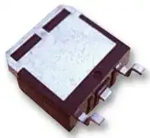
IXFT140N10P
Power MOSFET, PolarFET, N Channel, 100 V, 140 A, 0.011 ohm, TO-268 (D3PAK), Surface Mount
⚠️ Reference pricing provided. In case of supply shortages, we will connect you with our trusted procurement partners to ensure your project's continuity.
- Manufacturer: IXYS SEMICONDUCTOR
- Product type: Single MOSFETs
- Transistor Polarity:N Channel; Continuous Drain Current Id:140A; Drain Source Voltage Vds:100V; On Resistance Rds(on):0.011ohm; Rds(on) Test Voltage Vgs:15V; Threshold Voltage Vgs:5V; Power Dissipation
- No. of Pins: 3Pins
- Channel Type: N Channel
- Product Range: -
- Qualification: -
- Power Dissipation: 600W
- Transistor Mounting: Surface Mount
- Rds(on) Test Voltage: 15V
- Transistor Case Style: TO-268 (D3PAK)
- Drain Source Voltage Vds: 100V
- Operating Temperature Max: 175°C
- Continuous Drain Current Id: 140A
- Drain Source On State Resistance: 0.011ohm
- Gate Source Threshold Voltage Max: 5V
| Delivery and price | |
|---|---|
| Units per pack | 800 |
| Price | 3.34 € |
| Current stock | 10+ |
| Lead time | 30 days |
Datasheet

## **PolarHV[TM] HiPerFET Power MOSFETs**

N-Channel Enhancement Mode Fast Intrinsic Diode Avalanche Rated

**IXFH 140N10P       V = 100 V DSS IXFT 140N10P        I = 140 A D25 R ≤ 11 m Ω DS(on) t ≤ 150 ns rr**

**==> picture [504 x 342] intentionally omitted <==**

**----- Start of picture text -----**<br>
|||||||||||||
|---|---|---|---|---|---|---|---|---|---|---|---|
|Symbol|Test Conditions|Maximum Ratings|TO-247 (IXFH)|
|VDSS|TJ|= 25|°|C to 175|°|C|100|V|
|VDGR|TJ|= 25|°|C to 175|°|C; RGS = 1 M|Ω|100|V|
|VGS|Continuous|±|20|V|
|IVD25GSM|TransientTC|= 25|°|C|140|±|30|AV|G D S|D (TAB)|
|I|External lead current limit|75|A|
|D(RMS)|
|IDM|TC|= 25|°|C, pulse width limited by TJM|300|A|TO-268 (IXFT)|
|IAR|TC|= 25|°|C|60|A|
|EAR|TC|= 25|°|C|80|mJ|
|EAS|TC|= 25|°|C|2.5|J|G|nit|
|S|D (TAB)|
|dv/dt|IS|≤|IDM, di/dt|≤|100 A/|µ|s, VDD|≤|VDSS,|10|V/ns|
|TJ|≤|150|°|C, RG = 4|Ω|G = Gate|D = Drain|
|PD|TC|= 25|°|C|600|W|S = Source|TAB = Drain|
|TJ|-55 ... +175|°|C|
|TJM|175|°|C|
|T|-55 ... +150|°|C|
|stg|
|TL|1.6 mm (0.062 in.) from case for 10 s|300|°|C|Features|
|TSOLD|Plastic body for 10s|260|°|C|l|International standard packages|
|Md|Mounting torque|(TO-247)|1.13/10|Nm/lb.in.|l|Unclamped Inductive Switching (UIS)|
|rated|
|Weight|TO-247TO-268|6.05.0|gg|l|Low package inductance-|
|easy to drive and to protect|

**----- End of picture text -----**<br>


## **Advantages**

**==> picture [434 x 151] intentionally omitted <==**

**----- Start of picture text -----**<br>
||||||||||
|---|---|---|---|---|---|---|---|---|
|Symbol|Test Conditions|Characteristic Values|
|(TJ = 25|°|C, unless otherwise specified)|Min.    Typ.|Max.|l|Easy to mount|
|l|Space savings|
|BVDSS|VGS|= 0 V, ID = 250|µ|A|100|||V|l|
|High power density|
|VGS(th)|VDS|= VGS, ID = 4.0 mA                                  3.0|_|5.0|V|
|IGSS|VGS|=|±|20 VDC, VDS = 0|_|±|100|nA|
|IDSS|VDS|=  VDSS|25|µ|A|
|VGS = 0 V|TJ = 175|°|C|7|500|µ|A|
|RDS(on)|VGS|= 10 V, ID = 0.5 ID25|11|m|Ω|
|VGS|= 15 V, ID = 300 A|9|m|Ω|
|Note 1|

**----- End of picture text -----**<br>


DS99213E(01/06)

© 2006 IXYS All rights reserved

**IXFH 140N10P IXFT 140N10P**

**==> picture [339 x 424] intentionally omitted <==**

**----- Start of picture text -----**<br>
||||||||
|---|---|---|---|---|---|---|
|Symbol|Test Conditions                                                Characteristic Values|
|(TJ = 25|°|C, unless otherwise specified)|
|Min.|Typ.|Max.|
|gfs|VDS= 10 V; ID = 0.5 ID25, Note 1|45|65|S|
|Ciss|4700|pF|
|Coss|VGS = 0 V, VDS = 25 V, f = 1 MHz|1850|pF|
|Crss|600|pF|
|t|35|ns|
|d(on)|
|tr|VGS = 10 V, VDS = 0.5 VDSS, ID = 60 A|50|ns|
|td(off)|RG = 4|Ω|(External)|85|ns|
|tf|26|ns|
|Q|155|nC|
|g(on)|
|Qgs|VGS= 10 V, VDS = 0.5 VDSS, ID = 0.5 ID25|33|nC|
|Q|85|nC|
|gd|
|RthJC|0.25|°|C/W|
|RthCS|(TO-247)|0.21|°|C/W|
|Source-Drain Diode                                                                Characteristic Values|
|(TJ = 25|°|C, unless otherwise specified)|
|Symbol|Test Conditions|Min.|Typ.|Max.|
|IS|VGS = 0 V|140|A|
|ISM|Repetitive|300|A|
|VSD|IF = IS, VGS = 0 V,|1.5|V|
|Pulse test, t|≤|300|µ|s, duty cycle d|≤|2 %|
|trr|IF = 25 A,  -di/dt = 100 A/|µ|s|150|200|ns|
|QRM|VR = 50 V, VGS = 0 V|0.8|µ|C|
|IRM|6|A|

**----- End of picture text -----**<br>


Note 1: Pulse test, t ≤ 300 µ s, duty cycle d ≤ 2 %

## **TO-247 AD Outline**

**==> picture [116 x 258] intentionally omitted <==**

**----- Start of picture text -----**<br>
|||||||
|---|---|---|---|---|---|
|1       2       3|
|Terminals:|1 - Gate|2 - Drain|
|3 - Source|Tab - Drain|
|Dim.|Millimeter|Inches|
|Min.|Max.|Min.|Max.|
|A|4.7|5.3|.185|.209|
|A1|2.2|2.54|.087|.102|
|A2|2.2|2.6|.059|.098|
|b|1.0|1.4|.040|.055|
|b1|1.65|2.13|.065|.084|
|b2|2.87|3.12|.113|.123|
|C|.4|.8|.016|.031|
|D|20.80|21.46|.819|.845|
|E|15.75|16.26|.610|.640|
|e|5.20|5.72|0.205|0.225|
|L|19.81|20.32|.780|.800|
|L1|4.50|.177|
|∅|P|3.55|3.65|.140|.144|
|Q|5.89|6.40|0.232|0.252|
|R|4.32|5.49|.170|.216|
|S|6.15|BSC|242|BSC|

**----- End of picture text -----**<br>


**==> picture [159 x 153] intentionally omitted <==**

**----- Start of picture text -----**<br>
 TO-268 Outline<br>**----- End of picture text -----**<br>


**==> picture [511 x 198] intentionally omitted <==**

**----- Start of picture text -----**<br>
||||||||||
|---|---|---|---|---|---|---|---|---|
|IXYS reserves the right to change limits, test conditions,  and  dimensions.|
|IXYS MOSFETs  and IGBTs are covered  by|4,835,592|4,931,844|5,049,961|5,237,481|6,162,665|6,404,065 B1|6,683,344|6,727,585|
|one or moreof the following U.S. patents:|4,850,072|5,017,508|5,063,307|5,381,025|6,259,123 B1|6,534,343|6,710,405B2|6,759,692|
|4,881,106|5,034,796|5,187,117|5,486,715|6,306,728  B1|6,583,505|6,710,463|6,771,478 B2|

**----- End of picture text -----**<br>


**IXFH 140N10P IXFT 140N10P**

**==> picture [243 x 432] intentionally omitted <==**

**----- Start of picture text -----**<br>
Fig. 1. Output Characteristics<br>@ 25ºC<br>140<br>VGS = 10V<br>120           9V<br>100<br>80<br>8V<br>60<br>7V<br>40<br>20<br>6V<br>0<br>0 0.2 0.4 0.6 0.8 1 1.2 1.4 1.6<br>VD S - Volts<br>Fig. 3. Output Characteristics<br>@ 150ºC<br>140<br>VGS = 10V<br>120           9V<br>100<br>8V<br>80<br>7V<br>60<br>40 6V<br>20<br>5V<br>0<br>0 0.4 0.8 1.2 1.6 2 2.4 2.8 3.2<br>VD S - Volts<br> - Amperes<br>D<br>I<br> - Amperes<br>D<br>I<br>**----- End of picture text -----**<br>


**Fig. 5. RDS(on) Normalized to 0.5 ID25 Value vs. Drain Current**

**==> picture [232 x 181] intentionally omitted <==**

**----- Start of picture text -----**<br>
3<br>2.75<br>2.5<br>TJ = 175ºC<br>2.25<br>2<br>1.75 V GS = 10V<br>1.5<br>VGS = 15V<br>1.25<br>TJ = 25ºC<br>1<br>0.75<br>0 50 100 150 200 250 300 350<br>I D - Amperes<br> - Normalized<br>D S ( o n )<br>R<br>**----- End of picture text -----**<br>


**Fig. 2. Extended Output Characteristics @ 25ºC**

**==> picture [229 x 183] intentionally omitted <==**

**----- Start of picture text -----**<br>
300<br>270 VGS = 10V<br>240<br>9V<br>210<br>180<br>150<br>8V<br>120<br>90<br>60 7V<br>30<br>6V<br>0<br>0 1 2 3 V4 D S - Volts5 6 7 8 9 10<br> - Amperes<br>D<br>I<br>**----- End of picture text -----**<br>


**Fig. 4. RDS(on) Normalized to 0.5 ID25 Value vs. Junction Temperature**

**==> picture [233 x 405] intentionally omitted <==**

**----- Start of picture text -----**<br>
2.4<br>2.2 VGS = 10V<br>2<br>1.8<br>1.6 ID = 140A<br>1.4<br>ID = 70A<br>1.2<br>1<br>0.8<br>0.6<br>-50 -25 0 25 50 75 100 125 150 175<br>TJ - Degrees Centigrade<br>Fig. 6. Drain Current vs. Case<br>Temperature<br>90<br>80 External Lead Current Limit<br>70<br>60<br>50<br>40<br>30<br>20<br>10<br>0<br>-50 -25 0 25 50 75 100 125 150 175<br>TC - Degrees Centigrade<br> - Normalized<br>D S ( o n )<br>R<br> - Amperes<br>D<br>I<br>**----- End of picture text -----**<br>


© 2006 IXYS All rights reserved

**IXFH 140N10P IXFT 140N10P**

**Fig. 7. Input Admittance**

**==> picture [230 x 184] intentionally omitted <==**

**----- Start of picture text -----**<br>
250<br>225<br>200<br>175<br>150<br>125<br>100<br>75  TJ = 150 º C<br>         25ºC<br>50<br>        -40ºC<br>25<br>0<br>4 4.5 5 5.5 6 6.5 7 7.5 8 8.5 9 9.5<br>VG S - Volts<br> - Amperes<br>D<br>I<br>**----- End of picture text -----**<br>


**Fig. 9. Source Current vs. Source-To-Drain Voltage**

**==> picture [231 x 181] intentionally omitted <==**

**----- Start of picture text -----**<br>
300<br>250<br>200<br>150<br>100<br>TJ = 150ºC<br>50<br>TJ = 25ºC<br>0<br>0.4 0.6 0.8 1 1.2 1.4 1.6<br>VS D - Volts<br> - Amperes<br>S<br>I<br>**----- End of picture text -----**<br>


**Fig. 11. Capacitance**

**==> picture [232 x 182] intentionally omitted <==**

**----- Start of picture text -----**<br>
10000<br>Ciss<br>1000 Coss<br>C rss<br>f  = 1MHz<br>100<br>0 5 10 15 20 25 30 35 40<br>VDS - Volts<br>Capacitance - picoFarads<br>**----- End of picture text -----**<br>


**Fig. 8. Transconductance**

**==> picture [231 x 183] intentionally omitted <==**

**----- Start of picture text -----**<br>
90<br>80<br>70<br>60<br>50 TJ = -40 º C<br>40        25ºC<br>     150ºC<br>30<br>20<br>10<br>0<br>0 40 80 120 160 200 240 280 320<br>I D - Amperes<br> - Siemens<br>f s<br>g<br>**----- End of picture text -----**<br>


**Fig. 10. Gate Charge**

**==> picture [228 x 184] intentionally omitted <==**

**----- Start of picture text -----**<br>
10<br>9 VDS = 50V<br>8 ID = 70A<br>IG = 10mA<br>7<br>6<br>5<br>4<br>3<br>2<br>1<br>0<br>0 20 40 60 80 100 120 140 160<br>Q G - nanoCoulombs<br> - Volts<br>G S<br>V<br>**----- End of picture text -----**<br>


**Fig. 12. Forward-Bias Safe Operating Area**

**==> picture [234 x 182] intentionally omitted <==**

**----- Start of picture text -----**<br>
1000<br>T J  = 175ºC<br>R  Limit T C  = 25ºC<br>DS(on)<br>25µs<br>100µs<br>100<br>1ms<br>10ms<br>DC<br>10<br>1 10 100 1000<br>VD S - Volts<br> - Amperes<br>D<br>I<br>**----- End of picture text -----**<br>


IXYS reserves the right to change limits, test conditions,  and  dimensions.

**IXFH 140N10P IXFT 140N10P**

**==> picture [261 x 9] intentionally omitted <==**

**----- Start of picture text -----**<br>
Fig . 1 3 . M a x im u m  T r a n s ie n t T h e r m a l Re s is ta n c e<br>**----- End of picture text -----**<br>


**==> picture [491 x 176] intentionally omitted <==**

**----- Start of picture text -----**<br>
1 . 0 0<br>0 . 1 0<br>0 . 0 1<br>0 . 1 1 1 0 1 0 0 1 0 0 0<br>Pu ls e  W id th  - millis e c o n d s<br>ºC / W<br> -<br>( t h ) J C<br>R<br>**----- End of picture text -----**<br>


© 2006 IXYS All rights reserved
Updated at April 27, 2026
About Novapart
Novapart is a B2B electronic component broker specialising in stock shortages and cost reduction. We source hard-to-find parts and identify compliant alternatives across a catalogue of 410,000+ components from 500+ manufacturers.
Learn more →Stock Shortage Specialist
When a component is unavailable, discontinued or has an unacceptable lead time, we tap into our network of vetted European and Asian distributors to source what you need — without compromising on quality or traceability.
Request a quote →Compliant Alternatives
We identify pin-to-pin, electrically equivalent substitutes that meet the same certifications (RoHS, AEC-Q100, REACH) as your original specification — validated against datasheets, not just part numbers. Often at a lower cost.
BOM Analysis service →