
Image not available
Illustrative purposes only

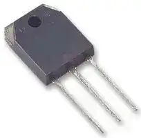
IXFQ28N60P3
Power MOSFET, N Channel, 600 V, 28 A, 0.26 ohm, TO-3P, Through Hole
⚠️ Reference pricing provided. In case of supply shortages, we will connect you with our trusted procurement partners to ensure your project's continuity.
- Manufacturer: IXYS SEMICONDUCTOR
- Product type: Single MOSFETs
- Transistor Polarity:N Channel; Continuous Drain Current Id:28A; Drain Source Voltage Vds:600V; On Resistance Rds(on):0.26ohm; Rds(on) Test Voltage Vgs:10V; Threshold Voltage Vgs:5V; Power
- MSL: MSL 1 - Unlimited
- SVHC: Lead (17-Jan-2023)
- No. of Pins: 3Pins
- Channel Type: N Channel
- Product Range: Polar3 HiPerFET
- Qualification: -
- Power Dissipation: 695W
- Transistor Mounting: Through Hole
- Rds(on) Test Voltage: 10V
- Transistor Case Style: TO-3P
- Drain Source Voltage Vds: 600V
- Operating Temperature Max: 150°C
- Continuous Drain Current Id: 28A
- Drain Source On State Resistance: 0.26ohm
- Gate Source Threshold Voltage Max: 5V
| Delivery and price | |
|---|---|
| Units per pack | 250 |
| Price | 2.98 € |
| Current stock | 10+ |
| Lead time | 30 days |
Datasheet

## **Polar3[TM ] HiperFET[TM] Power MOSFET** ## **IXFQ28N60P3 IXFH28N60P3** N-Channel Enhancement Mode Avalanche Rated Fast Intrinsic Rectifier **==> picture [353 x 283] intentionally omitted <==** **----- Start of picture text -----**<br> |||||| |---|---|---|---|---| |Symbol|Test Conditions|Maximum Ratings| |VDSS|TJ|= 25C to 150C|600|V| |VDGR|TJ|= 25C to 150C, RGS = 1M|600|V| |VGSS|Continuous| 30|V| |VGSM|Transient| 40|V| |ID25|TC|= 25C|28|A| |IDM|TC|= 25C, Pulse Width Limited by TJM|70|A| |IA|TC|= 25C|14|A| |EAS|TC|= 25C|500|mJ| |dv/dt|IS| IDM, VDD| VDSS, TJ| 150°C 35 V/ns| |PD|TC|= 25C|695|W| |T|-55 ... +150|C| |J| |TJM|150|C| |T|-55 ... +150|C| |stg| |TL|Maximum Lead Temperature for Soldering 300|°C| |TSOLD|1.6 mm (0.062in.) from Case for 10s 260|°C| |Md|Mounting Torque|1.13 / 10|Nm/lb.in| |Weight|TO-3P|5.5 g| |TO-247|6.0|g| **----- End of picture text -----**<br> **==> picture [352 x 123] intentionally omitted <==** **----- Start of picture text -----**<br> ||||||| |---|---|---|---|---|---| |Symbol|Test Conditions Characteristic Values| |(TJ = 25C Unless Otherwise Specified)|Min. Typ. Max.| |BVDSS|VGS|= 0V, ID = 1mA|600|||V| |VGS(th)|VDS|= VGS, ID = 2.5mA|3.0|5.0 V|||| |IGSS|VGS|= 30V, VDS = 0V|||||100 nA| |IDSS|VDS|= VDSS, VGS = 0V|25 A| |TJ = 125C|1.5|=|mA| |RDS(on)|VGS|= 10V, ID = 0.5 • ID25, Note 1|260 m|_|| **----- End of picture text -----**<br> **V = 600V DSS I = 28A D25 R 260m DS(on)** ## **TO-3P (IXFQ)** **==> picture [121 x 172] intentionally omitted <==** **----- Start of picture text -----**<br> G<br>D<br>S<br> Tab<br>TO-247 ( IXFH)<br>G<br>D Tab<br>S<br>G = Gate D = Drain<br>S = Source Tab = Drain<br>**----- End of picture text -----**<br> ## **Features** **==> picture [110 x 68] intentionally omitted <==** **----- Start of picture text -----**<br> ||| |---|---| ||Fast Intrinsic Rectifier| ||Avalanche Rated| ||Low RDS(ON) and QG| ||Low Package Inductance| |Advantages| **----- End of picture text -----**<br> **==> picture [88 x 67] intentionally omitted <==** **----- Start of picture text -----**<br> ||| |---|---| ||High Power Density| ||Easy to Mount| ||Space Savings| |Applications| **----- End of picture text -----**<br> **==> picture [144 x 67] intentionally omitted <==** **----- Start of picture text -----**<br> ||| |---|---| ||Switch-Mode and Resonant-Mode| |Power Supplies| ||DC-DC Converters| ||Laser Drivers| ||AC and DC Motor Drives| ||Robotics and Servo Controls| **----- End of picture text -----**<br> DS100322B(6/18) © 2018 IXYS CORPORATION, All Rights Reserved **IXFQ28N60P3 IXFH28N60P3** |**Symbol**<br>**Test Conditions**<br>**Characteristic Values**<br>|**Symbol**<br>**Test Conditions**<br>**Characteristic Values**<br>|**Symbol**<br>**Test Conditions**<br>**Characteristic Values**<br>| |---|---|---| |(TJ= 25C Unless Otherwise Specified)**Min.**|**Typ. **|**Max.**| |**gfs**<br>VDS = 20V, ID= 0.5 • ID25, Note 1 18|30|S| |**Ciss**<br> <br>**Coss**<br>VGS = 0V, VDS= 25V, f = 1MHz<br> <br>**Crss**<br>|3560<br>360<br>3.3|pF<br>pF<br>pF| |**RGi**<br>Gate Input Resistance<br>|1.5|| |**td(on)**<br> <br>**tr**<br> <br>**td(off)**<br> <br>**tf**<br> <br>**Resistive Switching Times**<br>VGS= 10V, VDS= 0.5 • VDSS, ID= 0.5 • ID25<br>RG= 1(External)|27<br>18<br>48<br>19|ns<br>ns<br>ns<br>ns| |**Qg(on)**<br> <br>**Qgs**<br>VGS = 10V, VDS= 0.5 • VDSS, ID= 0.5 • ID25<br> <br>**Qgd**<br>|50<br>17<br>14|nC<br>nC<br>nC| |**RthJC**<br>**RthCS**<br>|<br>0.25|0.18 C/W<br>C/W| ## **Source-Drain Diode** |**Symbol**<br>**Test Conditions**<br>**Characteristic Values**<br> |**Symbol**<br>**Test Conditions**<br>**Characteristic Values**<br> |**Symbol**<br>**Test Conditions**<br>**Characteristic Values**<br> | |---|---|---| |(TJ= 25C Unless Otherwise Specified)**Min.**|**Typ. **|**Max.**| |**IS**<br>VGS= 0V||28<br>A| |**ISM**<br>Repetitive, Pulse Width Limited by TJM||112<br>A| |**VSD**<br>IF= IS, VGS= 0V, Note 1||1.4<br>V| |**trr**<br> <br>**IRM** <br>**QRM**<br> <br>IF= 14A, -di/dt = 100A/s<br>VR= 100V, VGS = 0V|<br>9.0 <br>0.8|250 ns<br> A<br>μC| Note 1. Pulse test, t 300s, duty cycle, d 2%. IXYS Reserves the Right to Change Limits, Test Conditions, and Dimensions. IXYS MOSFETs and IGBTs are covered 4,835,592 4,931,844 5,049,961 5,237,481 6,162,665 6,404,065 B1 6,683,344 6,727,585 7,005,734 B2 7,157,338B2 by one or more of the following U.S. patents: 4,860,072 5,017,508 5,063,307 5,381,025 6,259,123 B1 6,534,343 6,710,405 B2 6,759,692 7,063,975 B2 4,881,106 5,034,796 5,187,117 5,486,715 6,306,728 B1 6,583,505 6,710,463 6,771,478 B2 7,071,537 **IXFQ28N60P3 IXFH28N60P3** **==> picture [264 x 214] intentionally omitted <==** **----- Start of picture text -----**<br> Fig. 1. Output Characteristics @ TJ = 25 [o] C<br>28<br>V GS = 10V<br> 8V<br>24<br>20 7V<br>16<br>12 6V<br>8<br>4<br>5V<br>0<br>0 1 2 3 4 5 6 7 8<br>VDS - Volts<br> - Amperes<br>ID<br>**----- End of picture text -----**<br> **==> picture [264 x 214] intentionally omitted <==** **----- Start of picture text -----**<br> Fig. 2. Extended Output Characteristics @ TJ = 25 [o] C<br>60<br>VGS = 10V<br> 8V<br>50<br>7V<br>40<br>30<br>20<br>6V<br>10<br>5V<br>0<br>0 5 10 15 20 25 30<br>VDS - Volts<br> - Amperes<br>ID<br>**----- End of picture text -----**<br> **==> picture [537 x 427] intentionally omitted <==** **----- Start of picture text -----**<br> Fig. 3. Output Characteristics @ TJ = 125 [o] C Fig. 4. RDS(on) Normalized to ID = 14A Value vs.<br>Junction Temperature<br>28 3.4<br>V GS = 10V<br>24 7V 3.0 VGS = 10V<br>2.6<br>20 6V I D = 28A<br>2.2<br>16<br>1.8 I D = 14A<br>12<br>1.4<br>8<br>1.0<br>5V<br>4<br>0.6<br>0 0.2<br>0 2 4 6 8 10 12 14 16 18 -50 -25 0 25 50 75 100 125 150<br>VDS - Volts TJ - Degrees Centigrade<br>Fig. 5. RDS(on) Normalized to ID = 14A Value vs.<br>Fig. 6. Maximum Drain Current vs. Case Temperature<br>Drain Current<br>3.4 32<br>V GS = 10V<br>3.0 T J = 125 [o] C 28<br>24<br>2.6<br>20<br>2.2<br>16<br>1.8<br>12<br>1.4 TJ = 25 [o] C<br>8<br>1.0<br>4<br>0.6 0<br>0 10 20 30 40 50 60 -50 -25 0 25 50 75 100 125 150<br>ID - Amperes TC - Degrees Centigrade<br> - Normalized<br> - Amperes<br>ID<br>DS(on)<br>R<br> - Normalized<br> - Amperes<br>ID<br>DS(on)<br>R<br>**----- End of picture text -----**<br> © 2018 IXYS CORPORATION, All Rights Reserved **IXFQ28N60P3 IXFH28N60P3** **==> picture [260 x 213] intentionally omitted <==** **----- Start of picture text -----**<br> Fig. 7. Input Admittance<br>50<br>40<br>TJ = 125 [o] C<br> 25 [o] C<br> - 40 [o] C<br>30<br>20<br>10<br>0<br>3.0 3.5 4.0 4.5 5.0 5.5 6.0 6.5 7.0<br>VGS - Volts<br> - Amperes<br>ID<br>**----- End of picture text -----**<br> **==> picture [260 x 213] intentionally omitted <==** **----- Start of picture text -----**<br> Fig. 9. Forward Voltage Drop of Intrinsic Diode<br>100<br>90<br>80<br>70<br>60<br>50<br>40<br>30 TJ = 125 [o] C<br>T J = 25 [o] C<br>20<br>10<br>0<br>0.3 0.4 0.5 0.6 0.7 0.8 0.9 1.0 1.1 1.2<br>VSD - Volts<br> - Amperes<br>IS<br>**----- End of picture text -----**<br> **==> picture [98 x 9] intentionally omitted <==** **----- Start of picture text -----**<br> Fig. 8. Transconductance<br>**----- End of picture text -----**<br> **==> picture [248 x 183] intentionally omitted <==** **----- Start of picture text -----**<br> 60<br>TJ = - 40 [o] C<br>50<br>25 [o] C<br>40<br>125 [o] C<br>30<br>20<br>10<br>0<br>0 10 20 30 40 50<br>ID - Amperes<br> - Siemens<br>f s<br>g<br>**----- End of picture text -----**<br> **Fig. 10. Gate Charge** **==> picture [251 x 185] intentionally omitted <==** **----- Start of picture text -----**<br> 10<br>9 VDS = 300V<br> I D = 14A<br>8<br> I G = 10mA<br>7<br>6<br>5<br>4<br>3<br>2<br>1<br>0<br>0 5 10 15 20 25 30 35 40 45 50<br>QG - NanoCoulombs<br> - Volts<br>GS<br>V<br>**----- End of picture text -----**<br> **Fig. 11. Capacitance** **Fig. 12. Forward-Bias Safe Operating Area** **==> picture [532 x 184] intentionally omitted <==** **----- Start of picture text -----**<br> 10,000 100<br>RDS(on) Limit<br>25μs<br>Ciss<br>100μs<br>1,000<br>10<br>C oss<br>100<br>1<br>10<br>T J = 150 [o] C<br>Crss TC = 25 [o] C 1ms<br>f = 1 MHz Single Pulse<br>1 0.1<br>0 5 10 15 20 25 30 35 40 10 100 1,000<br>VDS - Volts VDS - Volts<br> - Amperes<br>ID<br>Capacitance - PicoFarads<br>**----- End of picture text -----**<br> IXYS Reserves the Right to Change Limits, Test Conditions, and Dimensions. **IXFQ28N60P3 IXFH28N60P3** **Fig. 13. Maximum Transient Thermal Impedance** **==> picture [523 x 296] intentionally omitted <==** **----- Start of picture text -----**<br> 1<br>Fig. 13. Maximum Transient Thermal Impedance<br>AAAAA<br>0.3<br>0.1<br>0.01<br>0.001<br>0.00001 0.0001 0.001 0.01 0.1 1 10<br>Pulse Width - Seconds<br> - K / W<br> (th)JC<br>Z<br>**----- End of picture text -----**<br> © 2018 IXYS CORPORATION, All Rights Reserved IXYS REF: F_28N60P3(K7)03-26-12-A **IXFQ28N60P3 IXFH28N60P3** **==> picture [155 x 171] intentionally omitted <==** **----- Start of picture text -----**<br> TO-247 Outline<br>ete]— ee RT<br>Le<br>‘| Onl 02 (©)<br>ot<br>12 iL<br>ul 3s som<br>il |<br>;<br>cit Vi 1 - Gate<br>“ 2,4 - Drain<br>3 - Source<br>**----- End of picture text -----**<br> **==> picture [135 x 175] intentionally omitted <==** **----- Start of picture text -----**<br> TO-3P Outline E<br>| A oP<br>(/© [—\) af<br> OF<br>| D1<br>1% 3<br>uf aye<br>Tt<br>]<br>lye 1 - Gate<br>2,4 - Drain<br>at 3 - Source<br>**----- End of picture text -----**<br> IXYS Reserves the Right to Change Limits, Test Conditions, and Dimensions. **==> picture [157 x 46] intentionally omitted <==** Disclaimer Notice - Information furnished is believed to be accurate and reliable. However, users should independently evaluate the suitability of and test each product selected for their own applications. Littelfuse products are not designed for, and may not be used in, all applications. Read complete Disclaimer Notice at www.littelfuse.com/disclaimer-electronics.
Updated at April 27, 2026
About Novapart
Novapart is a B2B electronic component broker specialising in stock shortages and cost reduction. We source hard-to-find parts and identify compliant alternatives across a catalogue of 410,000+ components from 500+ manufacturers.
Learn more →Stock Shortage Specialist
When a component is unavailable, discontinued or has an unacceptable lead time, we tap into our network of vetted European and Asian distributors to source what you need — without compromising on quality or traceability.
Request a quote →Compliant Alternatives
We identify pin-to-pin, electrically equivalent substitutes that meet the same certifications (RoHS, AEC-Q100, REACH) as your original specification — validated against datasheets, not just part numbers. Often at a lower cost.
BOM Analysis service →