
Image not available
Illustrative purposes only

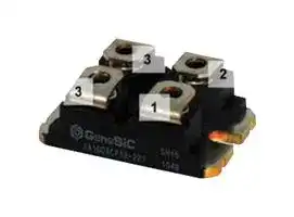
IXFN64N50P
Power MOSFET, PolarFET, N Channel, 500 V, 64 A, 0.085 ohm, ISOTOP, Module
⚠️ Reference pricing provided. In case of supply shortages, we will connect you with our trusted procurement partners to ensure your project's continuity.
- Manufacturer: IXYS SEMICONDUCTOR
- Product type: Single MOSFETs
- No. of Pins: 4Pins
- Channel Type: N Channel
- Power Dissipation: 700W
- Transistor Mounting: Module
- Transistor Polarity: N Channel
- Power Dissipation Pd: 700W
- Rds(on) Test Voltage: 10V
- On Resistance Rds(on): 0.085ohm
- Transistor Case Style: ISOTOP
- Drain Source Voltage Vds: 500V
- Operating Temperature Max: 150°C
- Continuous Drain Current Id: 64A
- Drain Source On State Resistance: 0.085ohm
- Gate Source Threshold Voltage Max: 5.5V
| Delivery and price | |
|---|---|
| Units per pack | 50 |
| Price | 19.51 € |
| Current stock | 10+ |
| Lead time | 30 days |
Datasheet

## **Polar[TM ] Power MOSFET HiPerFET[TM]**

## **IXFN64N50P**

N-Channel Enhancement Mode Avalanche Rated Fast Intrinsic Diode

|**Symbol**<br>**Test Conditions**<br>**Maximum Ratings**<br>**VDSS**<br>TJ = 25°C to 150°C<br>500<br>V<br>**VDGR**<br>TJ = 25°C to 150°C, RGS= 1MΩ<br>500<br>V<br>**VGSS**<br>Continuous<br>±30<br>V<br>**VGSM**<br>Transient<br>±40<br>V<br>~~— -~~<br>~~oo~~|**Symbol**<br>**Test Conditions**<br>**Maximum Ratings**<br>**VDSS**<br>TJ = 25°C to 150°C<br>500<br>V<br>**VDGR**<br>TJ = 25°C to 150°C, RGS= 1MΩ<br>500<br>V<br>**VGSS**<br>Continuous<br>±30<br>V<br>**VGSM**<br>Transient<br>±40<br>V<br>~~— -~~<br>~~oo~~|**Symbol**<br>**Test Conditions**<br>**Maximum Ratings**<br>**VDSS**<br>TJ = 25°C to 150°C<br>500<br>V<br>**VDGR**<br>TJ = 25°C to 150°C, RGS= 1MΩ<br>500<br>V<br>**VGSS**<br>Continuous<br>±30<br>V<br>**VGSM**<br>Transient<br>±40<br>V<br>~~— -~~<br>~~oo~~|**Symbol**<br>**Test Conditions**<br>**Maximum Ratings**<br>**VDSS**<br>TJ = 25°C to 150°C<br>500<br>V<br>**VDGR**<br>TJ = 25°C to 150°C, RGS= 1MΩ<br>500<br>V<br>**VGSS**<br>Continuous<br>±30<br>V<br>**VGSM**<br>Transient<br>±40<br>V<br>~~— -~~<br>~~oo~~|
|---|---|---|---|
|**ID25**<br>**IDM**|TC = 25°C<br>TC = 25°C, Pulse Width Limited by TJM|50<br>150|A<br>A|
|**IA**<br>**EAS**|TC = 25°C<br>TC = 25°C|64<br>2.5|A<br>J|
|**dV/dt**|IS<br>≤IDM,  VDD ≤VDSS, TJ ≤150°C|20|V/ns|
|**PD**|TC = 25°C|625|W|
|**TJ**<br>**TJM**<br>**Tstg**||-55 ... +150<br>150<br>-55 ... +150|°C<br>°C<br>°C|
|**TL**|1.6mm (0.062 in.) from Case for 10s|300|°C|
|**VISOL**|50/60 Hz, RMS                          t = 1min|2500|V~|
||IISOL ≤1mA                                  t = 1s|3000                  V~|3000                  V~|
|**Md**|Mounting Torque<br>1.5/13<br>Terminal Connection Torque|1.5/13<br>1.3/11.5         Nm/lb.in.|Nm/lb.in.<br>1.3/11.5         Nm/lb.in.|
|**Weight**||30|g|


**V =  500V DSS I =  50A D25 R ≤ 85m Ω DS(on) t ≤ 200ns rr**

**miniBLOC, SOT-227 B E153432** S G A — S D

G = Gate D = Drain S = Source

Either Source terminal at miniBLOC can be used as Main or Kelvin Source

## **Features**

International Standard Package miniBLOC, with Aluminium Nitride Isolation Isolation Voltage 2500 V~ Fast Intrinsic Diode Avalanche Rated Low R DS(on)

## **Advantages**

Low Gate Drive Requirement High Power Density

## **Applications:**

|**Symbol**<br>(T= 25°C, Unless Otherwise Specified)<br>**Min.      Typ.**|**Min.      Typ.**|**Max.**|
|---|---|---|
|(TJ= 25°C, Unless Otherwise Specified)<br>**Min.      Typ.**<br>~~r~~|**Min.      Typ. **<br>~~r~~|**Max.**|
|**BVDSS**<br>VGS = 0V, ID= 250μA<br>500<br>~~r~~|~~r~~|V|
|**VGS(th)**<br>VDS = VGS, ID= 8mA<br>3.0<br>~~r~~<br>~~|~~|5.5        V<br>~~r~~<br>~~_~~<br>~~||~~|5.5        V|
|**IGSS**<br>VGS =±30V, VDS= 0V<br>~~|~~|±<br>~~_~~<br>~~||~~|±200      nA|
|**IDSS**<br>VDS =  VDSS, VGS=  0V<br>TJ= 125°1     mA<br>~~|~~<br>~~|~~|25<br>1     mA<br>~~| |~~-<br>~~||~~|25μA<br>1     mA|
|**RDS(on)**<br>VGS = 10V, ID= 32A, Note 1<br>~~|~~|85     m<br>~~||~~|85     mΩ|


Switched-Mode and Resonant-Mode Power Supplies DC-DC Converters Laser Drivers AC and DC Motor Drives Robotics and Servo Controls

DS99349F(05/09)

© 2009 IXYS CORPORATION, All Rights Reserved

## **IXFN64N50P**

|**Symbol**<br>**Test Conditions**<br>**Characteristic Values**<br>  <br>|**Symbol**<br>**Test Conditions**<br>**Characteristic Values**<br>  <br>|**Symbol**<br>**Test Conditions**<br>**Characteristic Values**<br>  <br>|
|---|---|---|
|(TJ= 25°C, Unless Otherwise Specified)<br>**Min. **|**Typ.**|**Max.**|
|**gfs**<br>VDS = 20V, ID= 32A, Note 1                         30<br><br>|50<br>|S<br>|
|**Ciss**<br> <br>**Coss**<br>VGS = 0V, VDS= 25V, f = 1MHz<br> <br>**Crss**<br>|9700<br>970<br>30|nF<br>pF<br>pF|
|**td(on)**<br> <br>**tr**<br> <br>**td(off)**<br> <br>**tf**<br> <br>**Resistive Switching Times**<br>VGS= 10V, VDS= 0.5 • VDSS,  ID= 32A<br>RG= 2Ω(External)|30<br>25<br>85<br>22|ns<br>ns<br>ns<br>ns|


## **SOT-227B Outline**

|**Source-Drain Diode**|**Source-Drain Diode**|**Characteristic Values**|**Characteristic Values**|**Characteristic Values**||
|---|---|---|---|---|---|
||(TJ=|25°C, Unless Otherwise Specified)||||
|**Symbol**|**Test Conditions**|**Min. **|**Typ.**|**Max.**||
|**IS**|VGS= 0V|||64|A|
|**ISM**|Repetitive, Pulse Width Limited by TJM|||250|A|
|**VSD**|IF= 64A, VGS= 0V, Note 1|||1.5|V|
|**trr**<br>**QRM**<br>**IRM**|<br>  <br>IF= 25A, -di/dt = 100A/μs<br>VR= 100V|<br> <br>|<br>0.6<br> 6.0|200<br> <br>|ns<br>μC<br>A|


Note 1: Pulse Test, t ≤ 300μs; Duty Cycle, d ≤ 2%.

IXYS Reserves the Right to Change Limits, Test Conditions,  and  Dimensions.

IXYS MOSFETs  and IGBTs are covered 4,835,592 4,931,844 5,049,961 5,237,481 6,162,665 6,404,065 B1 6,683,344 6,727,585 7,005,734 B2    7,157,338B2 by one or more of the following U.S. patents: 4,850,072 5,017,508 5,063,307 5,381,025 6,259,123 B1 6,534,343 6,710,405 B2 6,759,692 7,063,975 B2 4,881,106 5,034,796 5,187,117 5,486,715 6,306,728 B1 6,583,505 6,710,463 6,771,478 B2 7,071,537

## **IXFN64N50P**

**==> picture [532 x 212] intentionally omitted <==**

**----- Start of picture text -----**<br>
Fig. 1. Output Characteristics Fig. 2. Extended Output Characteristics<br>@ 25ºC @ 25ºC<br>70 160<br>VGS = 10V V GS = 10V<br>60           8V 140          8V<br>7V<br>120<br>50<br>100<br>6V 7V<br>40<br>80<br>30<br>60<br>6V<br>20 40<br>5V<br>10 20 5V<br>0 0<br>0.0 1.0 2.0 3.0 4.0 5.0 6.0 7.0 0 5 10 15 20 25 30<br>VDS - Volts VDS - Volts<br> - AmperesID  - AmperesID<br>**----- End of picture text -----**<br>


## **Fig. 3. Output Characteristics @ 125ºC**

**Fig. 4. RDS(on) Normalized to ID = 32A Value vs. Junction Temperature**

**==> picture [528 x 388] intentionally omitted <==**

**----- Start of picture text -----**<br>
70 3.2<br>60 V         8V GS = 10V 3.02.8 VGS = 10V<br>        7V<br>2.6<br>50 2.4<br>6V 2.2 I D = 64A<br>40 2.0<br>1.8 I D = 32A<br>30 1.6<br>1.4<br>20 1.2<br>5V<br>1.0<br>10 0.8<br>0.6<br>0 0.4<br>0 2 4 6 8 10 12 14 16 -50 -25 0 25 50 75 100 125 150<br>VDS - Volts TJ - Degrees Centigrade<br>Fig. 5. RDS(on) Normalized to ID = 32A Value  Fig. 6. Maximum Drain Current vs.<br>vs. Drain Current Case Temperature<br>3.4 55<br>3.2 V GS = 10V  50<br>3.0 TJ = 125ºC 45<br>2.8<br>40<br>2.6<br>35<br>2.4<br>2.2 30<br>2.0 25<br>1.8 20<br>1.6<br>15<br>1.4<br>TJ = 25ºC 10<br>1.2<br>1.0 5<br>0.8 0<br>0 20 40 60 80 100 120 140 160 -50 -25 0 25 50 75 100 125 150<br>ID - Amperes TC - Degrees Centigrade<br> - Normalized<br> - Amperes<br>ID<br>DS(on)<br>R<br> - Normalized  - Amperes<br>ID<br>DS(on)<br>R<br>**----- End of picture text -----**<br>


© 2009 IXYS CORPORATION, All Rights Reserved

## **IXFN64N50P**

**==> picture [260 x 211] intentionally omitted <==**

**----- Start of picture text -----**<br>
Fig. 7. Input Admittance<br>90<br>80<br>70<br>60<br>50<br>T J = 125ºC<br>40           25 º C<br>- 40ºC<br>30<br>20<br>10<br>0<br>3.0 3.5 4.0 4.5 5.0 5.5 6.0 6.5<br>VGS - Volts<br> - Amperes<br>ID<br>**----- End of picture text -----**<br>


**Fig. 9. Forward Voltage Drop of Intrinsic Diode**

**==> picture [249 x 174] intentionally omitted <==**

**----- Start of picture text -----**<br>
240<br>220<br>200<br>180<br>160<br>140<br>120<br>100<br>80<br>60 TJ = 125ºC<br>40<br>20 TJ  = 25ºC<br>0<br>0.3 0.4 0.5 0.6 0.7 0.8 0.9 1.0 1.1 1.2 1.3 1.4 1.5<br>VSD - Volts<br> - Amperes<br>IS<br>**----- End of picture text -----**<br>


**==> picture [262 x 422] intentionally omitted <==**

**----- Start of picture text -----**<br>
Fig. 8. Transconductance<br>90<br>80 TJ = - 40ºC<br>70<br>60 25ºC<br>50<br>125ºC<br>40<br>30<br>20<br>10<br>0<br>0 20 40 60 80 100 120 140<br>ID - Amperes<br>Fig. 10. Gate Charge<br>10<br>9  VDS = 250V<br> I D = 32A<br>8<br> I G = 10mA<br>7<br>6<br>5<br>4<br>3<br>2<br>1<br>0<br>0 20 40 60 80 100 120 140 160<br>QG - NanoCoulombs<br> - Siemens<br>f s<br>g<br> - Volts<br>GS<br>V<br>**----- End of picture text -----**<br>


**Fig. 11. Capacitance**

**Fig. 12. Maximum Transient Thermal Impedance**

**==> picture [529 x 174] intentionally omitted <==**

**----- Start of picture text -----**<br>
100,000 1.000<br>f = 1 MHz<br>Ciss<br>10,000<br>1,000 0.100<br>Coss<br>100<br>C rss<br>10 0.010<br>0 5 10 15 20 25 30 35 40 0.001 0.01 0.1 1 10<br>VDS - Volts Pulse Width - Seconds<br> - ºC / W<br>(th)JC<br>Z<br>Capacitance - PicoFarads<br>**----- End of picture text -----**<br>


IXYS Reserves the Right to Change Limits, Test Conditions,  and  Dimensions.

IXYS REF: F_64N50P(9J)4-27-09
Updated at February 9, 2023
About Novapart
Novapart is a B2B electronic component broker specialising in stock shortages and cost reduction. We source hard-to-find parts and identify compliant alternatives across a catalogue of 410,000+ components from 500+ manufacturers.
Learn more →Stock Shortage Specialist
When a component is unavailable, discontinued or has an unacceptable lead time, we tap into our network of vetted European and Asian distributors to source what you need — without compromising on quality or traceability.
Request a quote →Compliant Alternatives
We identify pin-to-pin, electrically equivalent substitutes that meet the same certifications (RoHS, AEC-Q100, REACH) as your original specification — validated against datasheets, not just part numbers. Often at a lower cost.
BOM Analysis service →