
Image not available
Illustrative purposes only

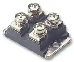
IXFN44N60
Power MOSFET, N Channel, 600 V, 44 A, 0.13 ohm, ISOTOP, Module
⚠️ Reference pricing provided. In case of supply shortages, we will connect you with our trusted procurement partners to ensure your project's continuity.
- Manufacturer: IXYS SEMICONDUCTOR
- Product type: Single MOSFETs
- No. of Pins: 3Pins
- Channel Type: N Channel
- Power Dissipation: 600W
- Transistor Mounting: Module
- Transistor Polarity: N Channel
- Power Dissipation Pd: 600W
- Rds(on) Test Voltage: 10V
- On Resistance Rds(on): 0.13ohm
- Transistor Case Style: ISOTOP
- Drain Source Voltage Vds: 600V
- Operating Temperature Max: 150°C
- Continuous Drain Current Id: 44A
- Drain Source On State Resistance: 0.13ohm
- Gate Source Threshold Voltage Max: 4.5V
| Delivery and price | |
|---|---|
| Units per pack | 100 |
| Price | 15.91 € |
| Current stock | 10+ |
| Lead time | 30 days |
Datasheet

## **HiPerFET[TM] Power MOSFETs Single Die MOSFET**

## **IXFN 44N60**

**V = 600 V DSS I = 44 A D25 RDS(on) =     130 m** 9) **t 250 ns** rr

|**Power MOSFETs**<br>**Single Die MOSFET**|**Power MOSFETs**<br>**Single Die MOSFET**||||**ID25**<br>**=**<br>**44    A**<br>**RDS(on) =     130 mDS(on) =     130 m =     130 m**<br>9)|
|---|---|---|---|---|---|
|N-Channel Enhancement Mode<br>Avalanche Rated, High dv/dt, Low trr|||D<br>S<br>G<br>S<br>&)||**t**rr<br>**250 ns**<br>,|
|**Symbol**|**Test Conditions**|**Maximum Ratings**||**Maximum Ratings**|**miniBLOC, SOT-227 B**|
||||||**E153432**|
|**VDSS**<br>**VDGR**|TJ = 25 C to 150 C<br>TJ = 25 C to 150 C; RGS= 1 M<br>°<br>°<br>Q||600<br>600|V<br>V|G<br>S|
|**VGS**<br>**VGSM**<br>**ID25**<br>**IDM**|Continuous<br>Transient<br>TC = 25 C<br>TC = 25 C, pulse width limited by TJM<br>°||20<br>30<br>44<br>176<br>4|V<br>V<br>A<br>A|S<br>D<br>a SA<br>Se”|
|**IAR**|TC = 25 C||44|A||
|**EAR**|TC = 25 C||60|mJ|G = Gate<br>D = Drain<br>S = Source<br>TAB = Drain|
|**EAS**|TC = 25 C||3|J|Either Source terminal at miniBLOC can be used|
|**dv/dt**|IS<br>IDM, di/dt 100 A/ s, VDD VDSS,<br>5<br><<br><<br>m<br><|||V/ns|as Main or Kelvin Source|
||TJ<br>150 C, RG= 2<br><<br>°<br>Q|||||
|**PD**|TC = 25 C||600|W|**Features**|
|**TJ**<br>**TJM**|-55 ... +150|-55 ... +150|-55 ... +150<br>150|C<br>C|• International standard package<br>• miniBLOC, with Aluminium nitride<br>isolation|
|**Tstg**||-55 ... +150|-55 ... +150|C|• Low RDS (on)HDMOSTMprocess|
|**TJ**<br>**VISOL**|1.6 mm (0.63 in) from case for 10 s<br>50/60 Hz, RMS<br>t = 1 min<br>IISOL1 mA<br>t = 1 s<br><||-<br>2500<br>3000|C<br>V~<br>V~|• Rugged polysilicon gate cell structure<br>• Unclamped Inductive Switching (UIS)<br>rated<br>• Low package inductance|
|**Md**|Mounting torque||1.5/13|Nm/lb.in.|• Fast intrinsic Rectifier|
||Terminal connection torque||1.5/13|Nm/lb.in.||
|**Weight**|||30|g|**Applications**|


## **Applications**

- DC-DC converters

## **Symbol Test Conditions Characteristic Values**

- Battery chargers

|||(TJ= 25 C, unless otherwise specified)<br>**min.**<br>**typ.**<br>**max.**|• Switched-mode and resonant-mode<br>power supplies|
|---|---|---|---|
|**VDSS**|VGS = 0 V, ID= 3 mA|600<br>V|• DC choppers|
|**VGH(th)**|VDS = VGS, ID= 8 mA|2.5<br>4.5<br>V|• Temperature and lighting controls|
|**IGSS**|VGS = 20 VDC, VDS= 0<br>100<br>nA<br>++|||
|**IDSS**|VDS =  VDSS|**Advantages**<br>TJ=   25 C<br>100<br>A<br>°<br>Ll||
||VGS = 0 V|TJ= 125 C<br>2<br>mA|• Easy to mount|
|**RDS(on)**|VGS = 10 V, ID= 0.5 • ID25||• Space savings|
||Pulse test, t  300 s, duty cycle d<br><<br>u|Pulse test, t  300 s, duty cycle d 2 %<br>130<br>m<br><<br>Q|•High power density|


- High power density

98610B (7/00)

IXYS reserves the right to change limits, test conditions, and dimensions.

© 2000 IXYS All rights reserved

1 - 4

**IXFN 44N60**

## **Symbol Test Conditions**

## **Characteristic Values**

|||(TJ= 25�|C, unless otherwise specified)|C, unless otherwise specified)|C, unless otherwise specified)|C, unless otherwise specified)|
|---|---|---|---|---|---|---|
||||**min.**|**typ.**|**max.**||
|**gfs**|VDS|= 10 V; ID= 0.5 • ID25, pulse test|30|45||S|
|**Ciss**||||8900||pF|
|**Coss**||VGS= 0 V, VDS= 25 V, f = 1 MHz||1000||pF|
|**Crss**||||330||pF|
|**td(on)**||||42||ns|
|**tr**||VGS= 10 V, VDS= 0.5 • VDSS, ID= 0.5 • ID25||55||ns|
|**td(off)**||RG= 1�(External),||110||ns|
|**tf**||||45||ns|
|**Qg(on)**||||330||nC|
|**Qgs**||VGS= 10 V, VDS= 0.5 • VDSS, ID= 0.5 • ID25||60||nC|
|**Qgd**||||65||nC|
|**RthJC**|||||0.21|K/W|
|**RthCK**||||0.05||K/W|


## **Source-Drain Diode**

## **Characteristic Values**

**miniBLOC, SOT-227 B**

|M4 screws (4x) supplied|M4 screws (4x) supplied|M4 screws (4x) supplied|
|---|---|---|
|Dim.|Millimeter<br>Min.<br>Max.<br>|Inches<br>Min.<br>Max.|
|A<br>3<br>B<br>|1.50<br>31.88<br>1.<br>7.80<br>8.20<br>0.|240<br>1.255<br>307<br>0.323|
|C<br><br>D<br>|4.09<br>4.29<br>0.<br>4.09<br>4.29<br>0.|161<br>0.169<br>161<br>0.169|
|E<br><br>F<br>1|4.09<br>4.29<br>0.<br>4.91<br>15.11<br>0.|161<br>0.169<br>587<br>0.595|
|G<br>3<br>H<br>3|0.12<br>30.30<br>1.<br>8.00<br>38.23<br>1.|186<br>1.193<br>496<br>1.505|
|J<br>1<br>K<br>|1.68<br>12.22<br>0.<br>8.92<br>9.60<br>0.|460<br>0.481<br>351<br>0.378|
|L<br><br>M<br>1|0.76<br>0.84<br>0.<br>2.60<br>12.85<br>0.|030<br>0.033<br>496<br>0.506|
|N<br>2<br>O<br>|5.15<br>25.42<br>0.<br>1.98<br>2.13<br>0.|990<br>1.001<br>078<br>0.084|
|P<br><br>Q<br>2|4.95<br>5.97<br>0.<br>6.54<br>26.90<br>1.|195<br>0.235<br>045<br>1.059|
|R<br><br>S<br>|3.94<br>4.42<br>0.<br>4.72<br>4.85<br>0.|155<br>0.174<br>186<br>0.191|
|T<br>2<br>U<br>-|4.59<br>25.07<br>0.<br>0.05<br>0.1<br>-0.|968<br>0.987<br>002<br>0.004|


|||(TJ= 25�C, unless otherwise specified)|(TJ= 25�C, unless otherwise specified)|(TJ= 25�C, unless otherwise specified)|(TJ= 25�C, unless otherwise specified)|
|---|---|---|---|---|---|
|**Symbol**|**Test Conditions**|**min.**|**typ.**|**max.**||
|**IS**|VGS = 0 V|||44|A|
|**ISM**|Repetitive;|||176|A|
||pulse width limited by TJM|||||
|**VSD**|IF= IS, VGS= 0 V,|||1.3|V|
||Pulse test, t�300�s, duty cycle d�2 %|||||
|**trr**|IF= 50A, -di/dt = 100 A/�s, VR= 100 V|||250|ns|
|**QRM**|||1.4||�C|
|**IRM**|||8||A|


IXYS MOSFETS and IGBTs are covered by one or more of the following U.S. patents: 4,835,592 4,881,106 5,017,508 5,049,961 5,187,117 5,486,715 4,850,072 4,931,844 5,034,796 5,063,307 5,237,481 5,381,025

© 2000 IXYS All rights reserved

2 - 4

**IXFN 44N60**

Figure 1. Output Characteristics at 25[O] C

Figure 2. Output Characteristics at 125[O] C

**==> picture [455 x 606] intentionally omitted <==**

**----- Start of picture text -----**<br>
100 80<br>TJ = 25 [O] C VGS = 10V TJ = 125 [O] C V          9VGS = 10V 6V<br>80           9V           8V<br>          8V 60           7V<br>          7V<br>          6V 5V<br>60<br>5V 40<br>40<br>20<br>20<br>0 0<br>0 4 8 12 16 20 24 0 4 8 12 16 20 24<br>VDS - Volts VDS - Volts<br>Figure  3. RDS(on) normalized to 15A/25 [O] C vs. ID Figure 4. RDS(on) normalized to 15A/25DS(on) normalized to 15A/25 [[O]]<br>2.4 2.4<br>VGS = 10V TJ = 125 [O] C VGS = 10V<br>2.0 2.0<br>ID = 44A<br>1.6 1.6<br>TJ = 25 [O] C ID = 22A<br>1.2 1.2<br>0.8 0.8<br>0 20 40 60 80 100 25 50 75 100 125 150<br>ID - Amperes TJ - Degrees C<br>Figure 5. Drain Current vs. Case Temperature Figure 6. Admittance Curves<br>60 60<br>50 50<br>40 40 TJ = 125 [o] C<br>30 30<br>20 20 TJ = 25 [o] C<br>10 10<br>0 0<br>-50 -25 0 25 50 75 100 125 150 3.0 3.5 4.0 4.5 5.0 5.5<br>TC - Degrees C VGS - Volts<br> - Amperes  - Amperes<br>ID ID<br> - Normalized  - Normalized<br>DS(ON) DS(ON)<br>R R<br> - AmperesID  - AmperesID<br>**----- End of picture text -----**<br>


normalized to 15A/25[[O]] C vs. T Figure 4. RDS(on) normalized to 15A/25DS(on) normalized to 15A/25 J

© 2000 IXYS All rights reserved

3 - 4

**IXFN 44N60**

**==> picture [100 x 11] intentionally omitted <==**

**----- Start of picture text -----**<br>
Figure 7. Gate Charge<br>**----- End of picture text -----**<br>


Figure 8. Capacitance Curves

**==> picture [474 x 179] intentionally omitted <==**

**----- Start of picture text -----**<br>
12 10000<br>Ciss<br>10 VDS = 300V f = 1MHz<br>   ID = 30A<br>   IG = 10mA<br>8<br>Coss<br>6 1000<br>4<br>2 Crss<br>0 100<br>0 50 100 150 200 250 300 350 400 0 5 10 15 20 25 30 35 40<br>Gate Charge - nC VDS - Volts<br> - Volts<br>GS<br>V<br>Capacitance - pF<br>**----- End of picture text -----**<br>


Figure 9. Forward Voltage Drop of the Intrinsic Diode

**==> picture [214 x 187] intentionally omitted <==**

**----- Start of picture text -----**<br>
100<br>80<br>TJ = 125 [O] C<br>60<br>40 TJ = 25 [O] C<br>20<br>0<br>0.2 0.4 0.6 0.8 1.0 1.2<br>VSD -  Volts<br> - Amperes<br>ID<br>**----- End of picture text -----**<br>


Figure 10. Transient Thermal Resistance

**==> picture [430 x 174] intentionally omitted <==**

**----- Start of picture text -----**<br>
1.00<br>0.10<br>0.01<br>0.00<br>10 [-4] 10 [-3] 10 [-2] 10 [-1] 10 [0] 10 [1]<br>Pulse Width - Seconds<br> - K/W<br>JC<br>R(th)<br>**----- End of picture text -----**<br>


© 2000 IXYS All rights reserved

4 - 4
Updated at February 9, 2023
About Novapart
Novapart is a B2B electronic component broker specialising in stock shortages and cost reduction. We source hard-to-find parts and identify compliant alternatives across a catalogue of 410,000+ components from 500+ manufacturers.
Learn more →Stock Shortage Specialist
When a component is unavailable, discontinued or has an unacceptable lead time, we tap into our network of vetted European and Asian distributors to source what you need — without compromising on quality or traceability.
Request a quote →Compliant Alternatives
We identify pin-to-pin, electrically equivalent substitutes that meet the same certifications (RoHS, AEC-Q100, REACH) as your original specification — validated against datasheets, not just part numbers. Often at a lower cost.
BOM Analysis service →