
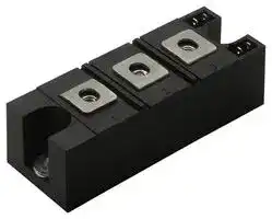


IRKT162/12PBF
THYRISTOR MODULE, 160A, 1200V
- Manufacturer: VISHAY
- Product type: Thyristors - SCR Modules
- SCR Module Type:Series Connected - SCRs; Peak Repetitive Off-State Voltage, Vdrm:1.2kV; Gate Trigger Current Max, Igt:150mA; Current It av:160A; On State RMS Current IT(rms):355A; Peak Non
- No. of Pins: 7Pins
- Product Range: -
- SCR Module Type: Series Connected - SCRs
- Thyristor Mounting: Panel
- On State RMS Current: 355A
- Thyristor Case Style: INT-A-PAK
- Average Forward Current: 160A
- Gate Trigger Current Max: 150mA
- Gate Trigger Voltage Max: 2.5V
- Operating Temperature Max: 125°C
- Repetitive Peak Reverse Voltage: 1.2kV
- Peak Repetitive Off State Voltage: 1.2kV
| Delivery and price | |
|---|---|
| Units per pack | 200 |
| Price | 52.62 € |
| Current stock | 10+ |
| Lead time | 30 days |
## **VSK.91.. Series** ~~—__——————————————EEESESESSSSSSSSS—S—SFSFSFSFMFSFSFSFSFSSSSSSSSSSSSSSTTUUUUCCM“#PUMNM——VW—S—CT~~ Vishay High Power Products CLL

## **ADD-A-PAK Generation VII Power Modules Thyristor/Diode and Thyristor/Thyristor, 95 A**

## **FEATURES**

- High voltage

- Industrial standard package

- UL pending

- 3500 VRMS isolating voltage

- Low thermal resistance

- Totally lead (Pb)-free

**==> picture [45 x 7] intentionally omitted <==**

**----- Start of picture text -----**<br>
ADD-A-PAK<br>**----- End of picture text -----**<br>


- Designed and qualified for industrial level

## **BENEFITS**

## **PRODUCT SUMMARY**

IT(AV) or IF(AV)

95 A

- Excellent thermal performances obtained by the usage of exposed direct bonded copper substrate

- Up to 1600 V

- High surge capability

## **MECHANICAL DESCRIPTION**

The ADD-A-PAK Generation VII, new generation of ADD-A-PAK module, combines the excellent thermal performances obtained by the usage of exposed direct bonded copper substrate, with advanced compact simple package solution and simplified internal structure with minimized number of interfaces.

- Easy mounting on heatsink

## **ELECTRICAL DESCRIPTION**

These modules are intended for general purpose high voltage applications such as high voltage regulated power supplies, lighting circuits, temperature and motor speed control circuits, UPS and battery charger.

## **MAJOR RATINGS AND CHARACTERISTICS**

**==> picture [447 x 150] intentionally omitted <==**

**----- Start of picture text -----**<br>
||||||||||
|---|---|---|---|---|---|---|---|---|
|SYMBOL|CHARACTERISTICS|VALUES|UNITS|
|IT(AV) or IF(AV)|85 °C|95|
|IO(RMS)|As AC switch|210|
|A|
|ITSM,|50 Hz|2000|
|IFSM|60 Hz|2094|
|50 Hz|20|
|I|[2]|t|kA|[2]|s|
|60 Hz|18.26|
|I|[2]|√|t|200|kA|[2]|√|s|
|VRRM|Range|400 to 1600|V|
|TStg|
|- 40 to 125|°C|
|TJ|

**----- End of picture text -----**<br>


For technical questions, contact: ind-modules@vishay.com

www.vishay.com 1

Document Number: 94632 Revision: 08-Dec-08

**VSK.91.. Series**

## Vishay High Power Products

## ADD-A-PAK Generation VII Power Modules Thyristor/Diode and Thyristor/Thyristor, 95 A

**==> picture [59 x 48] intentionally omitted <==**

## **ELECTRICAL SPECIFICATIONS**

## **VOLTAGE RATINGS**

|**VOLTAGE RATINGS**|**VOLTAGE RATINGS**|**VOLTAGE RATINGS**|**VOLTAGE RATINGS**|**VOLTAGE RATINGS**|**VOLTAGE RATINGS**|
|---|---|---|---|---|---|
|**TYPE NUMBER**|**VOLTAGE**<br>**CODE**|**VRRM, MAXIMUM**<br>**REPETITIVE PEAK**<br>**REVERSE VOLTAGE**<br>**V**|**VRSM, MAXIMUM**<br>**NON-REPETITIVE PEAK**<br>**REVERSE VOLTAGE**<br>**V**|**VDRM, MAXIMUM REPETITIVE**<br>**PEAK OFF-STATE VOLTAGE,**<br>**GATE OPEN CIRCUIT**<br>**V**|**IRRM,**<br>**IDRM**<br>**AT 125 °C**<br>**mA**|
|VSK.91|04|400|500|400|15|
||06|600|700|600||
||08|800|900|800||
||10|1000|1100|1000||
||12|1200|1300|1200||
||14|1400|1500|1400||
||16|1600|1700|1600||


## **ON-STATE CONDUCTION**

|**ON-STATE CONDUCTION**|**ON-STATE CONDUCTION**|**ON-STATE CONDUCTION**|**ON-STATE CONDUCTION**|**ON-STATE CONDUCTION**|**ON-STATE CONDUCTION**|**ON-STATE CONDUCTION**|
|---|---|---|---|---|---|---|
|**PARAMETER**|**SYMBOL**|**TEST CONDITIONS**|||**VALUES**|**UNITS**|
|Maximum average on-state current (thyristors)|IT(AV)|180° conduction, half sine wave,<br>TC= 85 °C|||95|A|
|Maximum average forward current (diodes)|IF(AV)||||||
|Maximum continuous RMS on-state current,<br>as AC switch|IO(RMS)|or<br>I(RMS)<br>I(RMS)|||210||
|Maximum peak, one-cycle non-repetitive<br>on-state or forward current|ITSM<br>or<br>IFSM|t = 10 ms|No voltage<br>reapplied|Sinusoidal<br>half wave,<br>initial TJ= TJmaximum|2000||
|||t = 8.3 ms|||2094||
|||t = 10 ms|100 % VRRM<br>reapplied||1682||
|||t = 8.3 ms|||1760||
|Maximum I2t for fusing|I2t|t = 10 ms|No voltage<br>reapplied|Initial TJ= TJmaximum|20|kA2s|
|||t = 8.3 ms|||18.26||
|||t = 10 ms|100 % VRRM<br>reapplied||14.14||
|||t = 8.3 ms|||12.91||
|Maximum I2√t for fusing|I2√t(1)|t = 0.1 ms to 10 ms, no voltage reapplied<br>TJ= TJmaximum|||200|kA2√s|
|Maximum value or threshold voltage|VT(TO) (2)|Low level(3)|TJ= TJmaximum||0.97|V|
|||High level(4)|||1.1||
|Maximum value of on-state<br>slope resistance|rt (2)|Low level(3)|TJ= TJmaximum||2.76|mΩ|
|||High level(4)|||2.38||
|Maximum peak on-state or forward voltage|VTM|ITM=πx IT(AV)|TJ= 25 °C||1.73|V|
||VFM|IFM=πx IF(AV)|||||
|Maximum non-repetitive rate of rise of<br>turned on current|dI/dt|TJ= 25 °C, from 0.67 VDRM,<br>ITM=πx IT(AV), Ig= 500 mA, tr< 0.5 µs, tp> 6 µs|||150|A/µs|
|Maximum holding current|IH|TJ= 25 °C, anode supply = 6 V,<br>resistive load,gate open circuit|||250|mA|
|Maximum latching current|IL|TJ= 25 °C, anode supply = 6 V, resistive load|||400||


## **Notes**

- (1) I2t for time tx = I2 √ t x √ tx

- (2) Average power = VT(TO) x IT(AV) + rt x (IT(RMS))2

- (3) 16.7 % x π x IAV < I < π x IAV

- (4) I > π x IAV

For technical questions, contact: ind-modules@vishay.com

Document Number: 94632 Revision: 08-Dec-08

www.vishay.com 2

**VSK.91.. Series**

**==> picture [59 x 48] intentionally omitted <==**

## ADD-A-PAK Generation VII Power Modules Thyristor/Diode and Thyristor/Thyristor, 95 A

## Vishay High Power Products

## **TRIGGERING**

|**TRIGGERING**|**TRIGGERING**|**TRIGGERING**|**TRIGGERING**|**TRIGGERING**|**TRIGGERING**|
|---|---|---|---|---|---|
|**PARAMETER**|**SYMBOL**|**TEST CONDITIONS**||**VALUES**|**UNITS**|
|Maximum peak gate power|PGM|||12|W|
|Maximum average gate power|PG(AV)|||3.0||
|Maximum peak gate current|IGM|||3.0|A|
|Maximum peak negative gate voltage|- VGM|||10|V|
|Maximum gate voltage required to trigger|VGT|TJ= - 40 °C|Anode supply = 6 V<br>resistive load|4.0||
|||TJ= 25 °C||2.5||
|||TJ= 125 °C||1.7||
|Maximum gate current required to trigger|IGT|TJ= - 40 °C|Anode supply = 6 V<br>resistive load|270|mA|
|||TJ= 25 °C||150||
|||TJ= 125 °C||80||
|Maximum gate voltage that will not trigger|VGD|TJ= 125 °C, rated VDRMapplied||0.25|V|
|Maximum gate current that will not trigger|IGD|TJ= 125 °C, rated VDRMapplied||6|mA|


## **BLOCKING**

|**BLOCKING**|**BLOCKING**|**BLOCKING**|**BLOCKING**|**BLOCKING**|
|---|---|---|---|---|
|**PARAMETER**|**SYMBOL**|**TEST CONDITIONS**|**VALUES**|**UNITS**|
|Maximum peak reverse and off-state<br>leakage current at VRRM, VDRM|IRRM,<br>IDRM|TJ= 125 °C, gate open circuit|15|mA|
|RMS insulation voltage|VINS|50 Hz, 1 s|3500|V|
|Maximum critical rate of rise of off-state voltage|dV/dt|TJ= 125 °C, linear to 0.67 VDRM|1000|V/µs|


## **THERMAL AND MECHANICAL SPECIFICATIONS**

|**THERMAL AND MECHANICAL SPECIFICATIONS**|**THERMAL AND MECHANICAL SPECIFICATIONS**|**THERMAL AND MECHANICAL SPECIFICATIONS**|**THERMAL AND MECHANICAL SPECIFICATIONS**|**THERMAL AND MECHANICAL SPECIFICATIONS**|**THERMAL AND MECHANICAL SPECIFICATIONS**|
|---|---|---|---|---|---|
|**PARAMETER**||**SYMBOL**|**TEST CONDITIONS**|**VALUES**|**UNITS**|
|Junction operating and storage<br>temperature range||TJ, TStg||- 40 to 125|°C|
|Maximum internal thermal resistance,<br>junction to case per leg||RthJC|DC operation|0.22|°C/W|
|Typical thermal resistance,<br>case to heatsink per module||RthCS|Mounting surface flat, smooth and greased|0.1||
|Mounting torque ± 10 %|to heatsink||A mounting compound is recommended and the<br>torque should be rechecked after a period of<br>3 hours to allow for the spread of the compound.|4|Nm|
||busbar|||3||
|Approximate weight||||75|g|
|||||2.7|oz.|
|Case style|||JEDEC|TO-240AA compatible||


## Δ **R CONDUCTION PER JUNCTION**

|Δ**R CONDUCTION PER JUNCTION**|Δ**R CONDUCTION PER JUNCTION**|Δ**R CONDUCTION PER JUNCTION**|Δ**R CONDUCTION PER JUNCTION**|Δ**R CONDUCTION PER JUNCTION**|Δ**R CONDUCTION PER JUNCTION**|Δ**R CONDUCTION PER JUNCTION**|Δ**R CONDUCTION PER JUNCTION**|Δ**R CONDUCTION PER JUNCTION**|Δ**R CONDUCTION PER JUNCTION**|Δ**R CONDUCTION PER JUNCTION**|Δ**R CONDUCTION PER JUNCTION**|
|---|---|---|---|---|---|---|---|---|---|---|---|
|**DEVICES**|**SINE HALF WAVE CONDUCTION**|||||**RECTANGULAR WAVE CONDUCTION**|||||**UNITS**|
||**180°**|**120°**|**90°**|**60°**|**30°**|**180°**|**120°**|**90°**|**60°**|**30°**||
|VSK.91..|0.04|0.048|0.063|0.085|0.125|0.033|0.052|0.067|0.088|0.127|°C/W|


## **Note**

- Table shows the increment of thermal resistance RthJC when devices operate at different conduction angles than DC

For technical questions, contact: ind-modules@vishay.com

www.vishay.com 3

Document Number: 94632 Revision: 08-Dec-08

ADD-A-PAK Generation VII Power Modules Thyristor/Diode and Thyristor/Thyristor, 95 A

## **VSK.91.. Series**

## Vishay High Power Products

**==> picture [180 x 607] intentionally omitted <==**

**----- Start of picture text -----**<br>
130<br>RthJC (DC) = 0.22°C/W<br>120<br>110<br>100<br>90 180°<br>120°<br>90°<br>80<br>60°<br>30°<br>70<br>0 20 40 60 80 100<br>Average on-state current (A)<br>Fig. 1 - Current Ratings Characteristics<br>130<br>RthJC (DC) = 0.22°C/W<br>120<br>110<br>100<br>DC<br>90 180°<br>120°<br>90°<br>80<br>60°<br>30°<br>70<br>0 20 40 60 80 100 120 140 160<br>Average on-state current (A)<br>Fig. 2 - Current Ratings Characteristics<br>160<br>180°<br>140 120°<br>90°<br>120 60°<br>30°<br>100<br>RMS limit<br>80<br>60<br>40<br>20<br>Per leg, Tj = 125°C<br>0<br>0 20 40 60 80 100<br>Average on-state current (A)<br>Fig. 3 - On-State Power Loss Characteristics<br>Maximum allowable case temperature (°C)<br>Maximum allowable case temperature (°C)<br>Maximum average on-state power loss (W)<br>**----- End of picture text -----**<br>


**==> picture [59 x 48] intentionally omitted <==**

**==> picture [195 x 607] intentionally omitted <==**

**----- Start of picture text -----**<br>
220<br>180°<br>200<br>120°<br>180 90°<br>160 60°<br>30° DC<br>140<br>120<br>RMS limit<br>100<br>80<br>60<br>40<br>20 Per leg, Tj = 125°C<br>0<br>0 20 40 60 80 100 120 140 160<br>Average on-state current (A)<br>Fig. 4 - On-State Power Loss Characteristics<br>1800<br>At any rated load condition and with<br>rated Vrrm applied following surge<br>1600 Initial Tj = Tj max<br>  @ 60  Hz 0.0083 s<br>@ 50 Hz 0.0100s<br>1400<br>1200<br>1000<br>Per leg<br>800<br>1 10 100<br>Number of equal amplitude half cycle current pulses (N)<br>Fig. 5 - Maximum Non-Repetitive Surge Current<br>2000<br>Maximum Non-repetitive Surge Current<br>1800 Versus Pulse Train Duration. Control<br>of conduction may not be maintained.<br>Initial Tj = 125°C<br>1600<br>No Voltage Reapplied<br>Rated Vrrm reapplied<br>1400<br>1200<br>1000<br>Per leg<br>800<br>0.01 0.1 1<br>Pulse train duration (s)<br>Fig. 6 - Maximum Non-Repetitive Surge Current<br>Maximum average on-state power loss (W)<br>Peak half sine wave on-state current (A)<br>Peak half sine wave on-state current (A)<br>**----- End of picture text -----**<br>


For technical questions, contact: ind-modules@vishay.com

Document Number: 94632 Revision: 08-Dec-08

www.vishay.com 4

## **VSK.91.. Series** ADD-A-PAK Generation VII Power Modules Vishay High Power Products wv ~~a~~ Thyristor/Diode and Thyristor/Thyristor, 95 A

**==> picture [339 x 595] intentionally omitted <==**

**----- Start of picture text -----**<br>
400<br>RthSA = 0.1 °C/W<br>350 180° 0.2 °C/W<br>0.3 °C/W<br>120°<br>300 Hor 90° SANS 0.5 °C/W0.7 °C/W HE<br>60° 1 °C/W<br>250 30° 1.5 °C/W<br>3 °C/W<br>200<br>On J ES<br>150<br>100<br>VSK.91 Series<br>50 Per module<br>Tj = 125°C<br>0<br>0 40 80 120 160 200 2400 20 40 60 80 100 120 140<br>Total RMS output current (A) Maximum allowable ambient temperature (°C)<br>Fig. 7 - On-State Power Loss Characteristics<br>700<br>RthSA = 0.1 °C/W<br>180°<br>0.2 °C/W<br>600 T E (sine) E Ae 0.3 °C/W<br>180° 0.5 °C/W<br>500 (rect) 1 °C/W<br>2 °C/W<br>400<br>∼ AES<br>300<br>fo RX<br>200<br>Lo<br>2 x VSK.91 Series<br>100 single phase bridge connected<br>Tj = 125°C<br>a NO<br>0<br>0 50 100 150 2 0 0 20 40 60 80 100 120 140<br>Total output current (A) Maximum allowable ambient temperature (°C)<br>Fig. 8 - On-State Power Loss Characteristics<br>900<br>RthSA = 0.1 °C/W<br>800 OOo 0.2 °C/W a<br>0.3 °C/W<br>700 0.5 °C/W<br>1 °C/W<br>600 120° Ty T E<br>500 ee (rect) WN TT<br>4 //<br>400 ET HE RREE<br>300 IK RK<br>200<br>3 x VSK.91 Series<br>100 7 three phase bridge connected ES<br>Tj = 125°C<br>Po SS)<br>0<br>0 40 80 120 160 200 2400 20 40 60 80 100 120 140<br>Total output current (A) Maximum allowable ambient temperature (°C)<br>Fig. 9 - On-State Power Loss Characteristics<br>Maximum total on-state power loss (W)<br>Maximum total power loss (W)<br>Maximum total power loss (W)<br>**----- End of picture text -----**<br>


For technical questions, contact: ind-modules@vishay.com

www.vishay.com

Document Number: 94632 Revision: 08-Dec-08

5

**VSK.91.. Series**

## Vishay High Power Products

ADD-A-PAK Generation VII Power Modules Thyristor/Diode and Thyristor/Thyristor, 95 A

**==> picture [59 x 48] intentionally omitted <==**

**==> picture [181 x 170] intentionally omitted <==**

**----- Start of picture text -----**<br>
1000<br>Per leg<br>100<br>10<br>Tj = 125°C<br>Tj = 25°C<br>1<br>0.5 1.0 1.5 2.0 2.5 3.0 3.5<br>Instantaneous on-state voltage (V)<br>Instantaneous on-state current (A)<br>**----- End of picture text -----**<br>


Fig. 10 - On-State Voltage Drop Characteristics

**==> picture [321 x 391] intentionally omitted <==**

**----- Start of picture text -----**<br>
1<br>Steady state value<br>RthJC = 0.22 °C/W<br>(DC operation)<br>0.1<br>0.01 Per leg<br>0.001<br>0.001 0.01 0.1 1 10<br>Square wave pulse duration (s)<br>Fig. 11 - Thermal Impedance ZthJC Characteristics<br>100<br>Rectangular gate pulse (1) PGM = 200 W, tp = 300 µs<br>a)Recommended load line for (2) PGM = 60 W, tp = 1 ms<br>rated di/dt: 20 V, 20 ohms<br>tr = 0.5 µs, tp >= 6 µs  (3) PGM = 30 W, tp = 2 ms<br>b)Recommended load line for (4) PGM = 12 W, tp = 5 ms<br><= 30% rated di/dt: 15 V, 40 ohms<br>10 tr = 1 µs, tp >= 6 µs (a)<br>(b)<br>1<br>(4) (3) (2) (1)<br>VGD<br>IGD<br>IRK.71../.91.. SeriesVSK. Frequency Limited by PG(AV)<br>0.1<br>0.001 0.01 0.1 1 10 100 1000<br>Instantaneous gate current (A)<br>Fig. 12 - Gate Characteristics<br> (°C/W)<br>thJC<br>Transient thermal impedance Z<br>TJ = -40 °C<br>TJ = 25 °C<br>TJ = 125 °C<br>Instantaneous gate voltage (V)<br>**----- End of picture text -----**<br>


For technical questions, contact: ind-modules@vishay.com

Document Number: 94632 Revision: 08-Dec-08

www.vishay.com 6

**VSK.91.. Series**

ADD-A-PAK Generation VII Power Modules Thyristor/Diode and Thyristor/Thyristor, 95 A

**==> picture [59 x 48] intentionally omitted <==**

## Vishay High Power Products

## **ORDERING INFORMATION TABLE**

|**Device code**|**VSK**|**VSK**||**T**<br>**91**|**/**|**16**||
|---|---|---|---|---|---|---|---|
|||1||3<br>2||4||
||**1**||-|Module type||||
|||||||||
||**2**||-|Circuit configuration (see end of datasheet)||||
|||||||||
||**3**||-|Current code (95 A)||||
|||||||||
||**4**||-|Voltage code (see Voltage Ratings table)||||


## **Note**

• To order the optional hardware go to www.vishay.com/doc?95172

## **CIRCUIT CONFIGURATION**

**==> picture [442 x 166] intentionally omitted <==**

**----- Start of picture text -----**<br>
VSKT VSKH VSKL VSKN<br>(1)~ (1)~ (1)~ (1)-<br>1 1 1 1<br>2 + 2 + 2 + 2 +<br>(2) (2) (2) (2)<br>3 3 3 3<br>4 5 7 6 4 5 7 6 4 5<br>- - - +<br>(3) (3) (3) (3)<br>G1 K1 K2 G2 G1 K1 K2 G2 G1 K1<br>(4) (5) (7) (6) (4) (5) (7) (6) (4) (5)<br>**----- End of picture text -----**<br>


|||
|---|---|
|**LINKS TO RELATED DOCUMENTS**||
|Dimensions|http://www.vishay.com/doc?95368|


For technical questions, contact: ind-modules@vishay.com

www.vishay.com 7

Document Number: 94632 Revision: 08-Dec-08

**Legal Disclaimer Notice**

Vishay

**==> picture [60 x 50] intentionally omitted <==**

## **Disclaimer**

All product specifications and data are subject to change without notice.

Vishay Intertechnology, Inc., its affiliates, agents, and employees, and all persons acting on its or their behalf (collectively, “Vishay”), disclaim any and all liability for any errors, inaccuracies or incompleteness contained herein or in any other disclosure relating to any product.

Vishay disclaims any and all liability arising out of the use or application of any product described herein or of any information provided herein to the maximum extent permitted by law. The product specifications do not expand or otherwise modify Vishay’s terms and conditions of purchase, including but not limited to the warranty expressed therein, which apply to these products.

No license, express or implied, by estoppel or otherwise, to any intellectual property rights is granted by this document or by any conduct of Vishay.

The products shown herein are not designed for use in medical, life-saving, or life-sustaining applications unless otherwise expressly indicated. Customers using or selling Vishay products not expressly indicated for use in such applications do so entirely at their own risk and agree to fully indemnify Vishay for any damages arising or resulting from such use or sale. Please contact authorized Vishay personnel to obtain written terms and conditions regarding products designed for such applications.

Product names and markings noted herein may be trademarks of their respective owners.

Document Number: 91000 Revision: 18-Jul-08

www.vishay.com 1
Updated at June 7, 2026
Vishay is a global leader in the manufacturing of discrete semiconductors and passive electronic components. Renowned for its exceptional quality and engineering expertise, the company produces highly reliable solutions that drive innovation across the industrial, automotive, telecommunications, and consumer electronics markets. From advanced factory automation to vehicle electrification, Vishay components provide the foundational building blocks for modern electronic design. The company's expansive portfolio is heavily focused on efficient power management, signal routing, and energy storage. Within its passive component lineup, Vishay is recognized for its extensive array of high-performance capacitors, including robust aluminium electrolytic, film, and polymer variants, alongside highly efficient power inductors. In the realm of discrete semiconductors, Vishay is a premier manufacturer of single and dual MOSFETs, as well as a vast selection of Schottky, Zener, and fast-recovery rectifier diodes designed for demanding power applications. Furthermore, Vishay delivers industry-leading circuit protection and thermal management solutions. With a broad offering of transient voltage suppressors (TVS diodes) and temperature-sensing NTC thermistors, these components are engineered to safeguard sensitive circuitry against both electrical and thermal overstress. By combining this vital mix of advanced discretes and passives, Vishay enables engineers to develop robust, space-saving, and highly resilient electronic systems.
About Novapart
Novapart is a B2B electronic component broker specialising in stock shortages and cost reduction. We source hard-to-find parts and identify compliant alternatives across a catalogue of 410,000+ components from 500+ manufacturers.
Learn more →Stock Shortage Specialist
When a component is unavailable, discontinued or has an unacceptable lead time, we tap into our network of vetted European and Asian distributors to source what you need — without compromising on quality or traceability.
Request a quote →Compliant Alternatives
We identify pin-to-pin, electrically equivalent substitutes that meet the same certifications (RoHS, AEC-Q100, REACH) as your original specification — validated against datasheets, not just part numbers. Often at a lower cost.
BOM Analysis service →