


IRGS4610DPBF
IGBT, 16 A, 1.7 V, 77 W, 600 V, TO-263 (D2PAK), 3 Pins
- Manufacturer: INFINEON
- Product type: Single IGBTs
- DC Collector Current:16A; Collector Emitter Saturation Voltage Vce(on):1.7V; Power Dissipation Pd:77W; Collector Emitter Voltage V(br)ceo:600V; Transistor Case Style:TO-263; No. of Pins:3
- No. of Pins: 3Pins
- Product Range: -
- Power Dissipation: 77W
- Transistor Mounting: Surface Mount
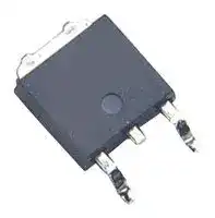
- Transistor Case Style: TO-263 (D2PAK)
- Operating Temperature Max: 175°C
- Continuous Collector Current: 16A
- Collector Emitter Voltage Max: 600V
- Collector Emitter Saturation Voltage: 1.7V
| Delivery and price | |
|---|---|
| Units per pack | 3000 |
| Price | 0.778 € |
| Current stock | 10+ |
| Lead time | 30 days |
**==> picture [493 x 145] intentionally omitted <==**

**----- Start of picture text -----**<br>
C C<br>Cc<br>= VcES =600V Cc ‘@<br>E<br>t. c NS C<br>Ictsc >10A,SUS, TimaxTc  == 100°C175°C G SG $.G Ne G<br>D-Pak<br>E D [2] -Pak<br>VcE(on)typ. = 1.7V@6A n-channel IRGR4610DPbF IRGS4610DPbF IRGB4610DPbF TO-220AB<br>G C E<br>Gate Collector Emitter<br>**----- End of picture text -----**<br>


- Appliance Drives

- Inverters

- UPS

|**G**<br>**C**<br>**E**<br>Gate<br>Collector<br>Emitter<br>• Appliance Drives<br>• Inverters<br>• UPS|**G**<br>**C**<br>**E**<br>Gate<br>Collector<br>Emitter<br>• Appliance Drives<br>• Inverters<br>• UPS|
|---|---|
|**Features**<br>**Benefits**<br>→||
|Low VCE(ON)and switchinglosses|Highefficiencyinawiderange ofapplications and switchingfrequencies|
|Square RBSOA and maximum junction temperature 175°C|Improved reliability due to rugged hard switching performance and higher<br>powercapability|
|Positive VCE(ON)temperature coefficient and tighter distribution of<br>parameters|Excellent current sharing in parallel operation|
|5μs short circuit SOA|Enables short circuit protection scheme|
|Lead-free,RoHS compliant|Environmentallyfriendly|


|**Base part number**|**Package Type**|**Standard Pack**|**Standard Pack**|**Orderable Part Number**|
|---|---|---|---|---|
|||**Form**|**Quantity**||
|IRGR4610DPbF|D-PAK|Tube|75|IRGR4610DPbF|
|||Tape and Reel|2000|IRGR4610DTRPbF|
|||Tape and Reel Right|3000|IRGR4610DTRRPbF|
|||Tape and Reel Left|3000|IRGR4610DTRLPbF|
|IRGS4610DPbF|D<br>2PAK|Tube|50|IRGS4610DPbF|
|||Tape and Reel Right|800|IRGS4610DTRRPbF|
|||Tape and Reel Left|800|IRGS4610DTRLPbF|
|IRGB4610DPbF|TO-220AB|Tube|50|IRGB4610DPbF|


## **Absolute Maximum Ratings**

|~~A~~|**Parameter**<br>|**Max.**<br>|**Units**<br>|
|---|---|---|---|
|VCES<br>~~se~~|Collector-to-Emitter Breakdown Voltage<br>~~se~~|600<br>~~se~~|V<br>~~se~~|
|IC@ TC= 25°C<br>~~se~~<br>~~GO~~|Continuous Collector Current<br>~~se~~<br>~~GO~~|16<br>~~se~~<br>~~GO~~|A<br>~~se~~<br>~~|_|~~|
|IC@ TC= 100°C<br>~~sO~~|Continuous Collector Current<br>~~sO~~|10<br>~~sO~~||
|ICM<br>~~a~~|Pulsed Collector Current,VGE= 15V<br>~~a~~|18<br>~~a~~||
|ILM<br>~~©~~|Clamped Inductive Load Current,VGE= 20V<br>~~©~~|24<br>~~©~~||
|IF@ TC= 25°C<br>~~sO~~|Diode Continuous Forward Current<br>~~sO~~|10<br>~~sO~~||
|IF@ TC=100°C<br>~~Ge~~|Diode Continuous Forward Current<br>~~Ge~~|6<br>~~Ge~~||
|IFM<br>~~rH~~|Diode Maximum Forward Current<br>~~rH~~|24<br>~~rH~~||
|VGE<br>~~Re~~<br>~~rH~~|Continuous Gate-to-Emitter Voltage<br>~~Re~~<br>~~rH~~|± 20<br>~~Re~~<br>~~rH~~|V<br>~~|_|~~|
||Transient Gate-to-Emitter Voltage<br>~~rH~~|± 30<br>~~rH~~||
|PD@ TC=25°<br>~~rH~~<br>~~Ge~~|Maximum Power Dissipation<br>~~rH~~<br>~~Ge~~|77<br>~~rH~~<br>~~Ge~~|W<br>~~|_|~~<br>~~eee~~|
|PD@ TC=100°<br>~~fe~~<br>~~ee~~|Maximum Power Dissipation<br>~~fe~~<br>~~ee~~|39<br>~~fe~~<br>~~eee~~||
|TJ<br>TSTG<br>~~fe~~<br>~~ee~~|Operating Junction and<br>Storage Temperature Range<br>~~fe~~<br>~~ee~~|-40 to + 175<br>~~fe~~<br>~~eee~~|°C<br>~~eee~~|
|~~ee~~|SolderingTemperature,for 10 seconds (1.6mm fromcase)<br>~~ee~~|300<br>~~eee~~||
|~~ee~~<br>~~A~~|MountingTorque, 6-32or M3 Screw        TO-220<br>~~ee ~~|10lbf. In(1.1 N.m)<br> ~~eee~~||


## ����������������

## **Thermal Resistance**

||**Parameter**|**Min.**|**Typ.**|**Max.**|**Units**|
|---|---|---|---|---|---|
|RθJC|Thermal Resistance, Junction-to-Case -(IGBT)�|–––|–––|1.9|°C/W|
|RθJC|Thermal Resistance, Junction-to-Case -(Diode)�|–––|–––|6.3||
|RθCS|Thermal Resistance,Case-to-Sink(flat, greased surface) (TO-220)|–––|0.5|–––||
|RθJA|Thermal Resistance, Junction-to-Ambient (PCB mount) (D-PAK)�|–––|–––|50||
||Thermal Resistance, Junction-to-Ambient (D-PAK)|–––|–––|110||
||Thermal Resistance, Junction-to-Ambient (PCB mount, Steady State)<br>(D<br>2PAK)�|–––|–––|40||
||Thermal Resistance, Junction-to-Ambient ( Socket mount) (TO-220)|–––|–––|62||


## **Electrical Characteristics @ TJ = 25°C (unless otherwise specified)**

||**Parameter**|**Min.**|**Typ.**|**Max.**|**Units **|**Conditions**|
|---|---|---|---|---|---|---|
|V(BR)CES|Collector-to-Emitter Breakdown Voltage|600|—|—|V|VGE= 0V,Ic=100μA�|
|ΔV(BR)CES/ΔTJ|Temperature Coeff. of Breakdown Voltage|—|0.36|—|V/°C|VGE=0V,Ic= 250μA(25-175<br>oC )|
|VCE(on)|Collector-to-Emitter Saturation Voltage|—|1.7|2.0|V|IC= 6.0A,VGE= 15V,TJ= 25°C|
|||—|2.07|—||IC= 6.0A,VGE= 15V,TJ= 150°C|
|||—|2.14|—||IC= 6.0A,VGE= 15V,TJ= 175°C|
|VGE(th)|Gate Threshold Voltage|4.0|—|6.5|V|VCE= VGE,IC= 150μA|
|ΔVGE(th)/ΔTJ|Threshold Voltage temp. coefficient|—|-13|—|mV/°C|VCE= VGE,IC= 250μA(25-175<br>oC )|
|gfe|Forward Transconductance|—|5.8|—|S|VCE= 25V,IC= 6.0A,PW =80μS|
|ICES|Collector-to-Emitter Leakage Current|—|—|25|μA|VGE= 0V,VCE= 600V|
|||—|—|250||VGE= 0V,VCE= 600V,TJ=175°C|
|VFM|Diode Forward Voltage Drop|—|1.60|2.30|V|IF= 6.0A|
|||—|1.30|—||IF= 6.0A,TJ= 175°C|
|IGES|Gate-to-Emitter Leakage Current|—|—|±100|nA|VGE= ± 20 V|


Notes:

- VCC = 80% (VCES), VGE = 20V, L = 1.0mH, RG = 100 Ω.

- R θ is measured at TJ approximately 90°C �

- Refer to AN-1086 for guidelines for measuring V(BR)CES safely.

- Pulse width limited by max. junction temperature.

- Values influenced by parasitic L and C in measurement

- When mounted on 1" square PCB (FR-4 or G-10 Material). For recommended footprint and soldering techniques refer to application note #AN-994: http://www.irf.com/technical-info/appnotes/an-994.pdf

�� ������������ ������������������������������������� ������������������������� ���������������������������������

����������������

## **Switching Characteristics @ TJ = 25°C (unless otherwise specified)**

||**Parameter**|**Min.**|**Typ.**|**Max.**|**Units**|**Conditions**|
|---|---|---|---|---|---|---|
|Qg|Total Gate Charge(turn-on)|—|13|—|nC|IC= 6.0A<br>VCC= 400V<br>VGE= 15V|
|Qge|Gate-to-Emitter Charge(turn-on)|—|3.0|—|||
|Qgc|Gate-to-Collector Charge(turn-on)|—|6.4|—|||
|Eon|Turn-On SwitchingLoss|—|56|—|μJ|IC= 6.0A, VCC= 400V, VGE= 15V<br>RG= 47Ω, L=1mH, LS= 150nH, TJ= 25°C<br>Energylosses include tail and diode reverse recovery|
|Eoff|Turn-Off SwitchingLoss|—|122|—|||
|Etotal|Total SwitchingLoss|—|178|—|||
|td(on)|Turn-On delaytime|—|27|—|<br>ns|IC= 6.0A, VCC= 400V<br>RG= 47Ω, L=1mH, LS= 150nH<br>TJ= 25°C�|
|tr|Rise time|—|11|—|||
|td(off)|Turn-Off delaytime|—|75|—|||
|tf|Fall time|—|17|—|||
|Eon|Turn-On SwitchingLoss|—|140|—|<br>μJ|IC= 6.0A, VCC= 400V, VGE= 15V<br>RG= 47Ω, L=1mH, LS= 150nH, TJ= 175°C<br>Energylosses include tail and diode reverse recovery|
|Eoff|Turn-Off SwitchingLoss|—|189|—|||
|Etotal|Total SwitchingLoss|—|329|—|||
|td(on)|Turn-On delaytime|—|26|—|<br>ns|IC= 6.0A, VCC= 400V<br>RG= 47Ω, L=1mH, LS= 150nH<br>TJ= 175°C�|
|tr|Rise time|—|12|—|||
|td(off)|Turn-Off delaytime|—|95|—|||
|tf|Fall time|—|32|—|||
|Cies|Input Capacitance|—|350|—|pF|VGE= 0V<br>VCC= 30V<br>f = 1Mhz|
|Coes|Output Capacitance|—|29|—|||
|Cres|Reverse Transfer Capacitance|—|10|—|||
|RBSOA|Reverse Bias Safe Operating Area|FULL SQUARE||||TJ= 175°C, IC= 24A<br>VCC= 500V, Vp =600V<br>RG= 100Ω,VGE= +20V to 0V|
|SCSOA|Short Circuit Safe Operating Area|5|—|—|μs|VCC= 400V, Vp =600V<br>RG= 100Ω,VGE= +15V to 0V|
|Erec|Reverse recoveryenergyof the  diode|—|178|—|μJ|TJ= 175~~o~~C<br>VCC= 400V, IF= 6.0A<br>VGE= 15V,Rg= 47Ω,L=1mH,LS=150nH|
|trr|Diode Reverse recoverytime|—|74|—|ns||
|Irr|Peak Reverse RecoveryCurrent|—|12|—|A||


�� ����������� ������������������������������������� ������������������������� ����������������������������������

**==> picture [202 x 199] intentionally omitted <==**

**----- Start of picture text -----**<br>
1816 Pot | tl<br>14 Sa<br>12 TST<br>10 Pot IN<br>8<br>Pet ft KA<br>6 P| | | KX<br>4 Po NT<br>2 eea ee<br>0<br>25 50 75 100 125 150 175<br> TC (°C)<br>IC (A)<br>**----- End of picture text -----**<br>


**Fig. 1** - Maximum DC Collector Current vs. Case Temperature

**==> picture [206 x 193] intentionally omitted <==**

**----- Start of picture text -----**<br>
100<br>10 a Sih el 10μsec<br>100μsec<br>Sa Sree<br>DC<br>1<br>Tc = 25°C<br>Tj = 175°C Si Sst<br>Single Pulse<br>0.1 Sa<br>1 10 100 1000<br>VCE (V)<br>IC (A)<br>**----- End of picture text -----**<br>


**Fig. 3** - Forward SOA, TC = 25°C, TJ ≤ 175°C, VGE = 15V

**==> picture [198 x 201] intentionally omitted <==**

**----- Start of picture text -----**<br>
20<br>15 PoZan Top VGE = 18V<br>V  = 15V<br>GE<br>VGE = 12V<br>V  = 10V<br>GE<br>Bae Bottom VGE = 8.0V<br>10<br>5<br>pao<br>0 TES[$—————_—_—<br>0 2 4 6 8 10<br> VCE (V)<br>ICE (A)<br>**----- End of picture text -----**<br>


**Fig. 5** - Typ. IGBT Output Characteristics TJ = -40°C; tp = 80μs

**==> picture [204 x 460] intentionally omitted <==**

**----- Start of picture text -----**<br>
80<br>7060 NEPNINTEEt<br>50 Nee<br>40<br>eae<br>30<br>.<br>20<br>aw<br>10 Pet | ot EN<br>0 aN<br>25 50 75 100 125 150 175<br> TC (°C)<br>Fig. 2  - Power  Dissipation vs. Case<br>Temperature<br>100<br>10<br>||<br>Sect<br>1 Ser Sec<br>0 Saal asaaiili<br>10 100 1000<br>VCE (V)<br>Fig. 4  - Reverse Bias SOA<br>TJ = 175°C, VGE = 20V<br>Ptot (W)<br>IC A)<br>**----- End of picture text -----**<br>


**==> picture [198 x 199] intentionally omitted <==**

**----- Start of picture text -----**<br>
20<br>{fit Sa<br>15 | Top V ft GE = 18V<br>V  = 15V<br>GE<br>VGE = 12V<br>V  = 10V<br>GE<br>10 WA Bottom V GE  = 8.0V<br>5<br>An<br>0 EEEAT [ | | |<br>0 2 4 6 8 10<br> VCE (V)<br>ICE (A)<br>**----- End of picture text -----**<br>


**Fig. 6** - Typ. IGBT Output Characteristics TJ = 25°C; tp = 80μs

**==> picture [198 x 199] intentionally omitted <==**

**----- Start of picture text -----**<br>
20<br>Top VGE = 18V<br>V  = 15V<br>GE<br>VGE = 12V<br>V  = 10V<br>GE<br>15 Bottom V GE  = 8.0V<br>Th]<br>fan<br>10<br>pay<br>5<br>poo<br>0 FA<br>0 2 4 6 8 10<br> VCE (V)<br>ICE (A)<br>**----- End of picture text -----**<br>


**Fig. 7** - Typ. IGBT Output Characteristics TJ = 175°C; tp = 80μs

**==> picture [199 x 422] intentionally omitted <==**

**----- Start of picture text -----**<br>
10<br>8 ain<br>6 I CE  = 3.0A<br>fh ICE = 6.0A<br>4 I CE  = 12A<br>2 mia<br>0<br>5 10 15 20<br> VGE (V)<br>Fig. 9  - Typical VCE vs. VGE<br>TJ = -40°C<br>10<br>8<br>Tt]<br>ICE = 3.0A<br>6 tt I CE  = 6.0A<br>ICE = 12A<br>4 et<br>2<br>mies<br>0 | fT TT<br>5 10 15 20<br> VGE (V)<br>VCE (V)<br>VCE (V)<br>**----- End of picture text -----**<br>


**Fig. 11** - Typical VCE vs. VGE TJ = 175°C

**==> picture [196 x 193] intentionally omitted <==**

**----- Start of picture text -----**<br>
20<br>18<br>16<br>-40°C<br>14 ESE 25°C<br>175°C<br>12<br>SSi<br>10<br>8<br>6<br>Fe<br>4<br>2<br>0 a) Am<br>0.0 1.0 2.0 3.0<br> VF (V)<br>IF (A)<br>**----- End of picture text -----**<br>


**Fig. 8** - Typ. Diode Forward Characteristics tp = 80μs

**==> picture [209 x 422] intentionally omitted <==**

**----- Start of picture text -----**<br>
10 tt<br>8<br>6 I CE  = 3.0A<br>ot ICE = 6.0A<br>4 I CE  = 12A<br>RE<br>2<br>0<br>5 10 15 20<br> VGE (V)<br>Fig. 10  - Typical VCE vs. VGE<br>TJ = 25°C<br>20<br>18<br>TJ = 25°C<br>16 T J  = 175°C<br>oS<br>14<br>12 s/n<br>10<br>8 oe on<br>6<br>4<br>asec<br>2<br>0<br>an<br>4 6 8 10 12 14 16<br> VGE, Gate-to-Emitter Voltage (V)<br>VCE (V)<br>IC, Collector-to-Emitter Current  (A)<br>**----- End of picture text -----**<br>


**Fig. 12** - Typ. Transfer Characteristics VCE = 50V; tp = 10μs

**==> picture [200 x 199] intentionally omitted <==**

**----- Start of picture text -----**<br>
400<br>350 PT TA<br>300<br>e/a<br>250<br>Of<br>200 EOFF<br>150 ca aae<br>100 | EON<br>50 44 HER<br>0 2 4 6 8 10 12 14<br>IC (A)<br>Energy (μJ)<br>**----- End of picture text -----**<br>


**Fig. 13** - Typ. Energy Loss vs. IC

TJ = 175°C; L = 1mH; VCE = 400V, RG = 47 Ω ; VGE = 15V.

**==> picture [203 x 424] intentionally omitted <==**

**----- Start of picture text -----**<br>
220<br>200<br>EOFF<br>180<br>Se]<br>160<br>Lf<br>140 E ON<br>120 ef<br>TP<br>100<br>80 / |<br>a<br>60<br>0 25 50 75 100 125<br>Rg ( Ω )<br>Fig. 15  - Typ. Energy Loss  vs. RG<br> = 175°C; L = 1mH; VCE = 400V, ICE = 6.0A; VCE = 400V, ICE = 6.0A; V= 400V, ICE = 6.0A; VCE = 6.0A; V= 6.0A; VGE = 15V<br>3025 Pf fot fd<br>RG = 10 Ω<br>20 Pp<br>15 R G =  22 Ω<br>10 R G =  47 Ω<br>Ae<br>5 Ser R G =  100 Ω<br>|TT ft<br>0 ff ft<br>2 4 6 8 10 12 14<br>IF (A)<br>IRR (A)<br>Energy (μJ)<br>**----- End of picture text -----**<br>


TJ = 175°C; L = 1mH; VCE = 400V, ICE = 6.0A; VCE = 400V, ICE = 6.0A; V= 400V, ICE = 6.0A; VCE = 6.0A; V= 6.0A; VGE = 15V

**Fig. 17** - Typical Diode IRR vs. IF TJ = 175°C

**==> picture [197 x 194] intentionally omitted <==**

**----- Start of picture text -----**<br>
1000 SS<br>td OFF<br>Se<br>100<br>SS] t F<br>tdON<br>10<br>SS<br>tR<br>Pre<br>1 eteeeELee ee<br>2 4 6 8 10 12 14<br>IC (A)<br>Swiching Time (ns)<br>**----- End of picture text -----**<br>


**Fig. 14** - Typ. Switching Time vs. IC TJ = 175°C; L=1mH; VCE= 400V RG= 47 Ω ; VGE= 15V

**==> picture [210 x 428] intentionally omitted <==**

**----- Start of picture text -----**<br>
1000<br>tdOFF<br>FLL<br>100<br>—— tF<br>tdON<br>Se<br>10 a ae<br>tR<br>FR<br>1 es ee<br>0 25 50 75 100 125<br>RG ( Ω )<br>Fig. 16 - Typ. Switching Time vs. RG<br>TJ = 175°C; L=1mH; VCE= 400V<br>ICE= 6.0A; VGE= 15V<br>22<br>20<br>Ff | | ft<br>18<br>NESE<br>16<br>14<br>12<br>=  ERE 10<br>NE<br>8<br>6 PfttER<br>0 25 50 75 100 125<br>RG ( Ω)<br>Swiching Time (ns)<br>IRR (A)<br>**----- End of picture text -----**<br>


**Fig. 18** - Typical Diode IRR vs. RG TJ = 175°C; IF = 6.0A

**==> picture [504 x 669] intentionally omitted <==**

**----- Start of picture text -----**<br>
20 1200<br>18<br>TTT. IA CTT<br>1000<br>12A<br>16<br>10 Ω<br>HAH 1  22 Ω<br>800<br>14<br> 47 Ω<br>ys ae<br>12 TIA 600 (Ll 6.0A<br>10 100 Ω<br>yr an<br>400<br>8 3.0A<br>6 4Pree. 200 TL<br>0 200 400 600 800 1000 1200 0 500 1000 1500<br>diF /dt (A/μs) diF /dt (A/μs)<br>Fig. 19 - Typical Diode IRR vs. diF/dt Fig. 20  - Typical Diode QRR<br>VCC= 400V; VGE= 15V; VCC= 400V; VGE= 15V; TJ = 175°C<br>ICE= 6.0A; TJ = 175°C<br>350 20 50<br>300<br>To RG = 10 Ω 15 = Tsc f 40<br>250 Isc<br>RG = 22 Ω<br>200 HERS 10 NS 30<br>pet SL<br>RG = 47 Ω<br>150<br>Uae RG = 100 Ω 5 ene 20<br>100<br>50 AT,“LTT |] [| 0 24nnn| 10<br>2 4 6 8 10 12 14 8 10 12 14 16 18<br>IF (A) VGE (V)<br>Fig. 21  - Typical Diode ERR vs. IF Fig. 22 - Typ. VGE vs. Short Circuit Time<br>TJ = 175°C VCC=400V, TC =25°C<br>1000 16<br>Cies<br>14 VCES = 400V<br>=a - VCES = 300V +<br>12<br>100<br>Saaa5 10 annie<br>8<br>Coes<br>6<br>10<br>Sonne Ge e 4 annee<br>Cres<br>2<br>1 es ee 0 Anni<br>0 100 200 300 400 500 0 2 4 6 8 10 12 14<br>VCE (V) Q G, Total Gate Charge (nC)<br>IRR (A)<br>Energy (μJ)<br>VGE, Gate-to-Emitter Voltage (V)<br>QRR (nC)<br>Time (μs)<br>Capacitance (pF)<br>Current (A)<br>**----- End of picture text -----**<br>


**Fig. 23** - Typ. Capacitance vs. VCE VGE= 0V; f = 1MHz

**Fig. 24** - Typical Gate Charge vs. VGE ICE = 6.0A, L=600μH

**==> picture [440 x 469] intentionally omitted <==**

**----- Start of picture text -----**<br>
10<br>a a ee a a a | eee<br>1 D = 0.50<br>0.20<br>ee<br>0.1 ct 0.100.02 0.05 0.01 Cor τ J τ J τ 1 τ 1 R 1 R1 PF τ 2 τ R 22 R2 R τ 3 3 R τ 3 3 τ R4 TTT τ 4R 4 4 τ C τ || Ri 00.7262       0.0000760.7721       0.000810.(0°C/W415 ) 0 τ .i 000005(sec)<br>es ieee Tt 7 > =<br>Pt er} Ci=  Ci τ i / Ri i / Ri EY=H 0.4016       0.004929<br>0.01 ai SINGLE PULSE 0 eee eee ereet<br>( THERMAL RESPONSE )<br>Notes:<br>a a ee ee ee ee ee ee ee ee ee eee maaan<br>1. Duty Factor D = t1/t2<br>2. Peak Tj = P dm x Zthjc + Tc<br>FEHR0 F EEE EE pH ll<br>0.001<br>1E-006 1E-005 0.0001 0.001 0.01 0.1<br>t1 , Rectangular Pulse Duration (sec)<br>Fig 25.   Maximum Transient Thermal Impedance, Junction-to-Case (IGBT)<br>10<br>ne<br>D = 0.50<br>me eer<br>0 . 20 atmrEeeeek tT LTT<br>1 A<br>0.10<br>Ss a a a ce eee ee ee ee cel<br>———e 0 .0 5 rT | | gO A R 1R1 R 2R2 R 3R3 R 4R 4 Ri ( ° C/W) τ i (sec)<br>0.1 Ptp—ealSeer 0.02 0.01 ATIee τ J τ peppy J τ 1 Ci τ 1= τ i / Ri τ 2 τ 2 τ 3 τ 3 τ 4 τ 4 τ C τ a—____} 0.2195       0.0000231.7733       0.000165 2.9352       0.0014931.3704       0.013255 ||<br>Aa ee eeOO”,a eeOOOee eee Ci i / Ri eeseee<br>PT Notes: a ee ee i<br>SINGLE PULSE 1. Duty Factor D = t1/t2<br>( THERMAL RESPONSE ) 2. Peak Tj = P dm x Zthjc + Tc<br>A  A 0 ee  ee<br>0.01 th ull EE cull<br>1E-006 1E-005 0.0001 0.001 0.01 0.1<br>t1 , Rectangular Pulse Duration (sec)<br>Thermal Response ( Z thJC )<br>Thermal Response ( Z thJC )<br>**----- End of picture text -----**<br>


**Fig. 26.** Maximum Transient Thermal Impedance, Junction-to-Case (DIODE)

**==> picture [210 x 47] intentionally omitted <==**

**----- Start of picture text -----**<br>
L<br>VCC<br>DUT<br>0<br>1K<br>**----- End of picture text -----**<br>


**Fig.C.T.1** - Gate Charge Circuit (turn-off)

**Fig.C.T.3** - S.C.SOA Circuit

**Fig.C.T.5** - Resistive Load Circuit

**==> picture [175 x 83] intentionally omitted <==**

**----- Start of picture text -----**<br>
L<br>80 V + DUT<br>- 480V<br>Rg<br>**----- End of picture text -----**<br>


**Fig.C.T.2** - RBSOA Circuit

**Fig.C.T.4** - Switching Loss Circuit

**Fig.C.T.6** - Typical Filter Circuit  for V Measurement (BR)CES

**==> picture [209 x 256] intentionally omitted <==**

**----- Start of picture text -----**<br>
600 12<br>500 10<br>400 8<br>tf<br>300 6<br>{oT<br>90% ICE<br>200 4<br>5% ICE<br>100 ne 2<br>5% VCE<br>0 0<br>Eoff Loss<br>-100 -2<br>-0.2 0 0.2 0.4 0.6 0.8 1<br>time(μs)<br> (V)<br>CE<br>V<br>**----- End of picture text -----**<br>


**Fig. WF1** - Typ. Turn-off Loss Waveform @ TJ = 175°C using Fig. CT.4

**==> picture [212 x 247] intentionally omitted <==**

**----- Start of picture text -----**<br>
100 15<br>0 Q RR 10<br>tRR<br>-100 5<br>-200 0<br>ipsam 10%<br>Peak<br>-300 Peak -5<br>IRR<br>IRR<br>TW<br>-400 -10<br>-500 -15<br>-600 et -20<br>-0.05 0.05 0.15 0.25<br>time (μS)<br> (V)<br>F<br>V<br>**----- End of picture text -----**<br>


WF.3- Typ. Diode Recovery Waveform @ TJ = 175°C using CT.4

**==> picture [207 x 254] intentionally omitted <==**

**----- Start of picture text -----**<br>
600 30<br>500 tr 25<br>TEST<br>CURRENT<br>400 20<br>90% test<br>300 15<br>ano current<br>200 10<br>10% test<br>current<br>100 5<br>a a 5% VCE<br>0 0<br>Eon Loss<br>-100 -5<br>4.3 4.5 4.7<br>time (μs)<br> (V)<br>CE<br>V<br>**----- End of picture text -----**<br>


**Fig. WF2** - Typ. Turn-on Loss Waveform @ TJ = 175°C using Fig. CT.4

**==> picture [210 x 248] intentionally omitted <==**

**----- Start of picture text -----**<br>
500 80<br>450 VCE 70<br>400 60<br>350 50<br>300 40<br>250 i 30<br>ICE<br>200 20<br>150 + > 10<br>100 0<br>50 -10<br>0 —I -20<br>-2 -1 0 1 2 3 4 5 6 7 8<br>Time (uS)<br>Vce (V)<br>**----- End of picture text -----**<br>


WF.4- Typ. Short Circuit Waveform @ TJ = 25°C using CT.3

EXAMPLE: THIS IS AN IRFR120 PART NUMBER WITH ASSEMBLY INTERNATIONAL c ~~S~~ LOT CODE 1234 RECTIFIER IRFU120 DATE CODE ASSEMBLED ON WW 16, 1999 LOGO 916A YEAR 9 =  1999 IN THE ASSEMBLY LINE "A" 12 34 WEEK 16 LINE A ASSEMBLY LOT CODE

**==> picture [494 x 122] intentionally omitted <==**

**----- Start of picture text -----**<br>
TR TRR TRL<br>SOOO OO : oo O ©<br>16.3 ( .641 ) 16.3 ( .641 )<br>15.7 ( .619 ) 15.7 ( .619 )<br>12.1 ( .476 ) FEED DIRECTION 8.1 ( .318 ) FEED DIRECTION<br>11.9 ( .469 ) 7.9 ( .312 )<br>**----- End of picture text -----**<br>


NOTES :

## 1.  CONTROLLING DIMENSION : MILLIMETER.

2.  ALL DIMENSIONS ARE SHOWN IN MILLIMETERS ( INCHES ).

3.  OUTLINE CONFORMS TO EIA-481 & EIA-541.

**==> picture [373 x 223] intentionally omitted <==**

**----- Start of picture text -----**<br>
  13 INCH<br>Z O or G)<br>16 mm<br>NOTES :<br>**----- End of picture text -----**<br>


1. OUTLINE CONFORMS TO EIA-481.

THIS IS AN IRF530S WITH LOT CODE 8024 ASSEMBLED ON WW 02, 2000 IN THE ASSEMBLY LINE "L"

**==> picture [262 x 221] intentionally omitted <==**

**----- Start of picture text -----**<br>
PART NUMBER<br>INTERNATIONAL<br>YN<br>RECTIFIER F530S<br>LOGO<br>I¢aR 002.<br>DATE CODE<br>80 24<br>YEAR 0 =  2000<br>ASSEMBLY<br>LOT CODE VY b e WEEK 02<br>u u LINE L<br>PART NUMBER<br>INTERNATIONAL<br>S S<br>RECTIFIER F530S<br>LOGO I¢eaR P002 A DATE CODE<br>P =  DESIGNATES LEAD - FREE<br>80 24<br>PRODUCT (OPTIONAL)<br>ASSEMBLY P u<br>LOT CODE Tent YEAR 0 =  2000<br>L L WEEK 02<br>A =  ASSEMBLY SITE CODE<br>**----- End of picture text -----**<br>


## OR

## Dimensions are shown in millimeters (inches))

## TRR

1.60 (.063) 1.50 (.059) 1.60 (.063) 4.10 (.161) 1.50 (.059) 3.90 (.153) 0.368 (.0145) 0.342 (.0135) ~~4 lal :~~ FEED DIRECTION ________* 1.85 (.073) ~~ooo~~ 6 4/S ~~ol~~ 11.60 (.457) - i} ee 1.65 (.065) ~~|~~ 11.40 (.449) 24.30 (.957) 15.42 (.609) 23.90 (.941) 15.22 (.601) TRL o aos J 1.75 (.069) 10.90 (.429) 1.25 (.049) 10.70 (.421) 4.72 (.136) ~~=~~ 16.10 (.634) | ~~r~~ 4.52 (.178) 15.90 (.626)

## FEED DIRECTION

**==> picture [387 x 205] intentionally omitted <==**

**----- Start of picture text -----**<br>
13.50 (.532) 27.40 (1.079)<br>7) 12.80 (.504) 23.90 (.941) a ie<br>4<br>330.00 60.00 (2.362)<br>(14.173) aN g       MIN.<br>  MAX.<br>30.40 (1.197)<br>      MAX.<br>26.40 (1.039 7 ) F 4<br>24.40 (.961)<br>3<br>**----- End of picture text -----**<br>


NOTES :

1.   COMFORMS TO EIA-418.

2.   CONTROLLING DIMENSION: MILLIMETER.

3.   DIMENSION MEASURED @ HUB.

4.   INCLUDES FLANGE DISTORTION @ OUTER EDGE.

**==> picture [348 x 73] intentionally omitted <==**

**----- Start of picture text -----**<br>
EXAMPLE: THIS IS AN IRF1010<br>LOT CODE 1789 INTERNATIONAL PART NUMBER<br>ASSEMBLED ON WW 19, 2000 RECTIFIER I RF 1010<br>IN THE ASSEMBLY LINE "C" LOGO IR 019C<br>17 39 DATE CODE<br>YEAR 0 =  2000<br>Note: "P" in assembly line position ASSEMBLY<br>indicates "Lead - Free" LOT CODE WEEK 19<br>LINE C<br>**----- End of picture text -----**<br>


TO-220AB packages are not recommended for Surface Mount Application.

## **Qualification Information[† ]**

|**Qualification Information[† ]**|||
|---|---|---|
|**Qualification Level**|Industrial<br>(per JEDEC JESD47F)††||
|**Moisture Sensitivity Level**|D-Pak|MSL1|
||D<br>2Pak||
||TO-220|N/A|
|**RoHS Compliant**|Yes||


- Qualification standards can be found at International Rectifier’s web site: http://www.irf.com/product-info/reliability ††   Applicable version of JEDEC standard at the time of product release

|**Revision History**|**Revision History**|
|---|---|
|**Date**<br>~~a~~|**Comments**|
|11/14/2014|•Added note<br>IFMDiode Maximum Forward Current  on page 1.<br>•Removed note<br>switching losses test condition on page 3.<br>• Updated package outline on page 15.<br>®|


**IR WORLD HEADQUARTERS:** 101 N. Sepulveda Blvd., El Segundo, California 90245, USA To contact International Rectifier, please visit http://www.irf.com/whoto-call/
Updated at June 9, 2026
Infineon Technologies is a globally recognized leader in semiconductor solutions, renowned for driving innovation in power management, energy efficiency, and modern mobility. With a strong legacy of engineering excellence, the company provides highly reliable components designed to meet the rigorous demands of industrial, automotive, and advanced commercial applications. The core of our Infineon portfolio is centered on their industry-leading discrete semiconductors. We offer an extensive selection of single and dual MOSFETs, alongside a robust range of single IGBTs and advanced IGBT modules. These flagship power transistors are essential for high-efficiency power conversion and motor control, providing engineers with superior thermal performance and minimized switching losses. Beyond advanced field-effect transistors, the selection includes a comprehensive array of diodes and rectifiers, heavily featuring Schottky diodes, as well as fast-recovery and RF/PIN diodes. This power foundation is further supported by bipolar transistors, intelligent power modules, and thyristor SCR modules, delivering the critical building blocks required for complex power system designs. To support broader system integration, the portfolio also encompasses specialized solutions such as solid-state relays, AC/DC LED driver ICs, and Bluetooth communications modules. From high-power industrial rectifiers to wireless connectivity adapters, Infineon equips designers with the precision components needed to build efficient, scalable, and fully connected electronic systems.
About Novapart
Novapart is a B2B electronic component broker specialising in stock shortages and cost reduction. We source hard-to-find parts and identify compliant alternatives across a catalogue of 410,000+ components from 500+ manufacturers.
Learn more →Stock Shortage Specialist
When a component is unavailable, discontinued or has an unacceptable lead time, we tap into our network of vetted European and Asian distributors to source what you need — without compromising on quality or traceability.
Request a quote →Compliant Alternatives
We identify pin-to-pin, electrically equivalent substitutes that meet the same certifications (RoHS, AEC-Q100, REACH) as your original specification — validated against datasheets, not just part numbers. Often at a lower cost.
BOM Analysis service →