
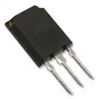


IRGPS46160DPBF
IGBT, 240 A, 1.7 V, 750 W, 600 V, TO-274AA, 3 Pins
- Manufacturer: INFINEON
- Product type: Single IGBTs
- DC Collector Current:240A; Collector Emitter Saturation Voltage Vce(on):1.7V; Power Dissipation Pd:750W; Collector Emitter Voltage V(br)ceo:600V; Transistor Case Style:TO-274AA; No. of Pins:
- No. of Pins: 3Pins
- Product Range: -
- Power Dissipation: 750W
- Transistor Mounting: Through Hole
- Transistor Case Style: TO-274AA
- Operating Temperature Max: 175°C
- Continuous Collector Current: 240A
- Collector Emitter Voltage Max: 600V
- Collector Emitter Saturation Voltage: 1.7V
| Delivery and price | |
|---|---|
| Units per pack | 250 |
| Price | 10.54 € |
| Current stock | 10+ |
| Lead time | 30 days |
_**INSULATED GATE BIPOLAR TRANSISTOR WITH**_ VCES = 600V _**ULTRAFAST SOFT RECOVERY DIODE**_ C C IC = 160A, TC = 100°C E tSC ≥ 5μs, TJ(max) = 175°C C G G VCE(on) typ. = 1.70V @ IC = 120A E Super-247 ~~—~~ n-channel **Applications** • Industrial Motor Drive **G C E** • Inverters Gate Collector Emitter • UPS • Welding **Features Benefits** High efficiency in a wide range of applications and switching Low VCE(ON) and Switching Losses frequencies Improved reliability due to rugged hard switching performance Square RBSOA and Maximum Junction Temperature 175°C and higher power capability ~~a~~ Positive VCE (ON) Temperature Coefficient Excellent current sharing in parallel operation ~~eG~~ 5μs short circuit SOA Enables short circuit protection scheme ~~a~~ Lead-Free, RoHS compliant Environmentally friendly

|**Form**<br>**Quantity**<br>**Base part number**<br>**Package Type**<br>**Standard Pack**<br>**Orderable part number**|**Form**<br>**Quantity**<br>**Base part number**<br>**Package Type**<br>**Standard Pack**<br>**Orderable part number**|**Orderable part number**||
|---|---|---|---|
|IRGPS46160DPbF<br>Super-247<br>Tube<br>25<br>IRGPS46160DPbF||||
|**Absolute Maximum Ratings**||||
|**Parameter**<br>**Max.**||**Units**||
|VCES<br>Collector-to-Emitter Voltage<br>600<br>V<br>IC @TC= 25°C<br>Continuous Collector Current<br>240<br>IC @TC= 100°C<br>Continuous Collector Current<br>160<br>ICM<br>Pulse Collector Current,VGE= 15V<br>360<br>ILM<br>Clamped Inductive Load  Current,VGE= 20V<br>480<br>A<br>IF @TC= 25°C<br>Diode Continous Forward Current<br>240<br>IF @TC= 100°C<br>Diode Continous Forward Current<br>160<br>IFM<br>Diode Maximum Forward Current<br>480<br>VGE<br>Continuous Gate-to-Emitter Voltage<br>±20<br>V<br>Transient Gate-to-Emitter Voltage<br>±30<br>PD @TC= 25°C<br>Maximum Power Dissipation<br>750<br>PD @TC= 100°C<br>Maximum Power Dissipation<br>375<br>TJ<br>Operating Junction and<br>-55 to +175<br>TSTG<br>Storage Temperature Range<br>°C<br>W<br>~~ee~~<br>~~ee~~<br>~~ee~~<br>~~Ee~~<br>~~ne~~<br>~~©~~<br>~~==~~<br>~~Ee©~~<br>~~©~~<br>~~Pe Ef~~<br>~~seffeseee~~<br>~~Ce~~<br>~~8~~<br>~~SSS~~<br>~~es~~<br>~~a~~||||
|Soldering Temperature, for 10 sec.<br>300 (0.063 in. (1.6mm) from case)||||
|Mounting Torque, 6-32 or M3 Screw<br>10 lbf·in (1.1 N·m)<br>~~DG~~||||
|**Thermal Resistance**||||
|**Parameter**<br>**Min.**<br>**Typ.**<br>**Max.**<br>**Units**<br>RθJC (IGBT)<br>Junction-to-Case(IGBT)<br>–––<br>–––<br>0.20<br>RθJC (Diode)<br>Junction-to-Case(Diode)<br>–––<br>–––<br>0.63<br>°C/W<br>~~DO~~<br>~~ee~~<br>~~ee~~||||
|RθCS<br>Case-to-Sink(flat, greased surface)<br>–––<br>0.24<br>–––||||
|RθJA<br>Junction-to-Ambient(typical socket mount)<br>–––<br>–––<br>40<br>~~A~~||||


## ��������������

## **Electrical Characteristics @ TJ = 25°C (unless otherwise specified)**

||**Parameter**|**Min.**|**Typ.**|**Max.**|**Units**|**Conditions**|
|---|---|---|---|---|---|---|
|V(BR)CES|Collector-to-Emitter Breakdown Voltage|600|—|—|V|VGE=0V,IC= 100μA�|
|ΔV(BR)CES/ΔTJ|Temperature Coeff. of Breakdown Voltage|—|0.27|—|V/°C|VGE =0V, IC =4.0mA (25°C-175°C)|
|VCE(on)|Collector-to-Emitter Saturation Voltage|—|1.70|2.05|V|IC= 120A,VGE= 15V,TJ= 25°C|
|||—|2.15|—||IC= 120A,VGE= 15V,TJ= 150°C|
|||—|2.20|—||IC= 120A,VGE= 15V,TJ= 175°C|
|VGE(th)|Gate Threshold Voltage|4.0|—|6.5|V|VCE= VGE,IC=5.6mA|
|ΔVGE(th)/ΔTJ|Threshold Voltage temp. coefficient|—|-17|—|mV/°C|VCE= VGE,IC=5.6mA(25°C- 175°C)|
|gfe|Forward Transconductance|—|77|—|S|VCE=50V,IC= 120A|
|ICES|Collector-to-Emitter Leakage Current|—|1.0|150|μA|VGE=0V,VCE=600V|
|||—|2.3|—|mA|VGE=0V,VCE=600V,TJ= 175°C|
|VFM|Diode Forward Voltage Drop|—|2.4|3.0|V|IF =120A|
|||—|1.9|—||IF= 120A,TJ= 175°C|
|IGES|Gate-to-Emitter LeakageCurrent|—|—|±400|nA|VGE= ±20V|


## **Switching Characteristics @ TJ = 25°C (unless otherwise specified)**

||**Parameter**|**Min.**|**Typ.**|**Max.**|**Units**|**Conditions**|
|---|---|---|---|---|---|---|
|Qg|Total Gate Charge|—|240|—|nC|IC= 120A<br>VGE= 15V<br>VCC= 400V|
|Qge|Gate-to-EmitterCharge|—|70|—|||
|Qgc|Gate-to-CollectorCharge|—|90|—|||
|Eon|Turn-OnSwitchingLoss|—|5750|—|μJ|IC= 120A, VCC= 400V, VGE= 15V<br>RG= 4.7Ω, L = 66μH, TJ= 25°C<br>Energy losses include tail<br>& diode reverse recovery�|
|Eoff|Turn-OffSwitchingLoss|—|3430|—|||
|Etotal|TotalSwitchingLoss|—|9180|—|||
|td(on)|Turn-On delaytime|—|80|—|<br>ns||
|tr|Rise time|—|70|—|||
|td(off)|Turn-Off delaytime|—|190|—|||
|tf|Fall time|—|40|—|||
|Eon|Turn-OnSwitchingLoss|—|7740|—|μJ|IC= 120A, VCC= 400V, VGE=15V<br>RG= 4.7Ω, L = 66μH, TJ= 175°C<br>Energy losses include tail<br>& diode reverse recovery�|
|Eoff|Turn-OffSwitchingLoss|—|4390|—|||
|Etotal|TotalSwitchingLoss|—|12130|—|||
|td(on)|Turn-On delay time|—|80|—|<br>ns||
|tr|Rise time|—|75|—|||
|td(off)|Turn-Off delaytime|—|230|—|||
|tf|Fall time|—|55|—|||
|Cies|InputCapacitance|—|7750|—|pF|VGE= 0V<br>VCC= 30V<br>f = 1.0Mhz|
|Coes|Output Capacitance|—|550|—|||
|Cres|Reverse TransferCapacitance|—|225|—|||
|RBSOA|Reverse Bias Safe Operating Area|FULL SQUARE||||TJ= 175°C, IC= 480A<br>VCC= 480V, Vp≤600V<br>Rg=4.7Ω, VGE =+20V to 0V|
|SCSOA|Short Circuit Safe Operating Area|5|—|—|μs|VCC= 400V, Vp≤600V<br>Rg= 4.7Ω,VGE= +15V to0V|
|Erec|Reverse RecoveryEnergyof the Diode|—|500|—|μJ|TJ= 175°C<br>VCC= 400V, IF= 120A<br>VGE= 15V,Rg= 4.7Ω,L = 100μH|
|trr|Diode Reverse RecoveryTime|—|130|—|ns||
|Irr|Peak Reverse Recovery Current|—|36|—|A||


## **Notes:**

- VCC = 80% (VCES), VGE = 20V, L = 66μH, RG = 4.7 Ω, tested in production ILM ≤ 400A.

- Pulse width limited by max. junction temperature.

- Refer to AN-1086 for guidelines for measuring V(BR)CES safely.

- R θ is measured at TJ of approximately 90°C.

- ������������������������������������������������������

- Calculated continuous current based on maximum allowable junction temperature. Package IGBT current limit is 195A. Package diode current limit is 120A.  Note that current limitations arising from heating of the device leads may occur.

�

�������������������������������������������������������������������������������� �����������������������������

**==> picture [436 x 187] intentionally omitted <==**

**----- Start of picture text -----**<br>
220<br>For both:<br>200 Poet TT Duty cycle : 50% Baal<br>Tj = 175°C<br>180 ee Baal<br>Tcase = 100°C<br>160 ee eee el Gate drive as specified ||<br>140 Pp—+ Square Wave: Ft TT TK Power Dissipation = 375W |<br>120 | | VCC iNN<br>100<br>I<br>| 2 Nl<br>80<br>| 7 Hi EE TT | ATT<br>60 ee<br>Diode as specified<br>| eee NS<br>40<br>eeeee<br>20 SS Ti TE NN<br>0.1 1 10 100<br>Load Current  ( A )<br>**----- End of picture text -----**<br>


f , Frequency ( kHz )

**Fig. 1** - Typical Load Current vs. Frequency (Load Current = IRMS of fundamental)

**==> picture [201 x 198] intentionally omitted <==**

**----- Start of picture text -----**<br>
250200 Sa<br>aN<br>150100 P|Py TINNG ||.<br>50 Py \<br>0 Py T y INP<br>25 50 75 100 125 150 175<br> TC (°C)<br>IC (A)<br>**----- End of picture text -----**<br>


**Fig. 2** - Maximum DC Collector Current vs. Case Temperature

**==> picture [208 x 194] intentionally omitted <==**

**----- Start of picture text -----**<br>
1000<br>10μsec<br>100<br>PZ CTI NCTE 100μsec mill<br>10 7 NICE TT<br>1msec<br>po Na a<br>1<br>Tc = 25°C<br>Tj = 175°C<br>Single Pulse DC<br>cut oN Co<br>0.1<br>1 10 100 1000 10000<br>VCE (V)<br>IC (A)<br>**----- End of picture text -----**<br>


**Fig. 4** - Forward SOA TC = 25°C, TJ ≤ 175°C; VGE =15V

**==> picture [204 x 193] intentionally omitted <==**

**----- Start of picture text -----**<br>
800<br>700<br>oo<br>600<br>ERNE<br>500 TANCE<br>400<br>ERERNEEE<br>300<br>200<br>ERNE<br>100<br>0 PFERRSeeeRNen tt} TN<br>0 20 40 60 80 100 120 140 160 180<br> TC (°C)<br>Ptot (W)<br>**----- End of picture text -----**<br>


**Fig. 3** - Power  Dissipation vs. Case Temperature

**==> picture [203 x 198] intentionally omitted <==**

**----- Start of picture text -----**<br>
1000<br>100<br>ervlees<br>10 en ll<br>en el<br>1<br>10 100 1000<br>VCE (V)<br>IC A)<br>**----- End of picture text -----**<br>


**Fig. 5** - Reverse Bias SOA TJ = 175°C; VGE =20V

**==> picture [198 x 198] intentionally omitted <==**

**----- Start of picture text -----**<br>
350<br>300<br>a (ee<br>250 Bae: \Qeeee<br>VGE = 18V<br>200 PASS VGE = 15V<br>VGE = 12V<br>VGE = 10V<br>150<br>pS VGE = 8.0V<br>100<br>Ee Ane aeee<br>50<br>Cpr<br>PF tt | | |<br>0<br>0 1 2 3 4 5 6 7 8 9 10<br> VCE (V)<br>ICE (A)<br>**----- End of picture text -----**<br>


**==> picture [199 x 450] intentionally omitted <==**

**----- Start of picture text -----**<br>
Fig. 6  - Typ. IGBT Output Characteristics<br>TJ = -40°C; tp = 80μs<br>350<br>300<br>P| ffi |<br>250<br>ae ene VGE = 18V<br>200 VGE = 15V<br>OS VGE = 12V<br>VGE = 10V<br>150<br>rf VGE = 8.0V<br>100 P p+ —<br>50<br>Cfo<br>0 A<br>0 2 4 6 8 10<br> VCE (V)<br>Fig. 8  - Typ. IGBT Output Characteristics<br>TJ = 175°C; tp = 80μs<br>25<br>2015 2ll I CE  = 6.0A<br>ICE = 120A<br>10 I CE  = 195A<br>| WW<br>5 Ml<br>PW<br>0<br>5 10 15 20<br> VGE (V)<br>ICE (A)<br>VCE (V)<br>**----- End of picture text -----**<br>


**Fig. 10** - Typical VCE vs. VGE TJ = -40°C

**==> picture [198 x 657] intentionally omitted <==**

**----- Start of picture text -----**<br>
350<br>300<br>iP<br>250 a ><a<br>VGE = 18V<br>VGE = 15V<br>200<br>PR VGE = 12V<br>VGE = 10V<br>150 VGE = 8.0V<br>| [o][f]<br>100 [#1]<br>| [f_|]<br>50<br>2a<br>0 yi<br>| | | |<br>0 2 4 6 8 10<br> VCE (V)<br>Fig. 7  - Typ. IGBT Output Characteristics<br>TJ = 25°C; tp = 80μs<br>600<br>500 -40°C ff<br>25°C<br>175°C<br>400<br>ee<br>any an<br>300<br>ff<br>200<br>Of<br>100<br>PL YZ [|]<br>po AnEE<br>0<br>0.0 1.0 2.0 3.0 4.0 5.0 6.0<br> VF (V)<br>Fig. 9  - Typ. Diode Forward Characteristics<br> tp = 80μs<br>25 a<br>20 I<br>15 I CE  = 6.0A<br>ICE = 120A<br>10 I CE  = 195A<br>Wee<br>(I<br>5 PW<br>0<br>5 10 15 20<br> VGE (V)<br>ICE (A)<br>IF (A)<br>VCE (V)<br>**----- End of picture text -----**<br>


**Fig. 11** - Typical VCE vs. VGE TJ = 25°C

**==> picture [209 x 193] intentionally omitted <==**

**----- Start of picture text -----**<br>
350<br>300<br>YT<br>TJ = -40°C<br>° C<br>250 TJ = 25<br>TJ = 175°C<br>ST |<br>200<br>150<br>TW<br>100<br>TATA<br>of / be<br>50<br>0 Ee | 4neee<br>3 4 5 6 7 8 9 10 11 12<br> VGE, Gate-to-Emitter Voltage (V)<br>IC, Collector-to-Emitter Current  (A)<br>**----- End of picture text -----**<br>


**==> picture [483 x 661] intentionally omitted <==**

**----- Start of picture text -----**<br>
25 350<br>300<br>Vii} YT<br>20 TJ = -40°C<br>° C<br>250 TJ = 25<br>TJ = 175°C<br>15 r\\\ I CE  = 6.0A 200 ST |<br>ICE = 120A<br>10 \\ I CE  = 195A 150 TW<br>100<br>Rive TATA<br>5<br>of / be<br>50<br>0 QS — 0 Ee | 4neee<br>5 10 15 20 3 4 5 6 7 8 9 10 11 12<br> VGE (V)  VGE, Gate-to-Emitter Voltage (V)<br>Fig. 12  - Typical VCE vs. VGE Fig. 13  - Typ. Transfer Characteristics<br>TJ = 175°C VCE = 50V; tp = 10μs<br>30000 1000<br>25000 P| | ft fy Se<br>tdOFF<br>20000<br>TTT —<br>EON<br>15000 100 tdON<br>10000 fy ———— t F<br>EOFF<br>5000<br>ra<br>tR<br>ae |<br>0 10 | | ft |<br>0 50 100 150 200 250 0 50 100 150 200 250<br>IC (A)<br>IC (A)<br>Fig. 14  - Typ. Energy Loss vs. IC Fig. 15  - Typ. Switching Time vs. IC<br>J = 175°C; L = 66μH; VCE = 400V, RG = 4.7 = 175°C; L = 66μH; VCE = 400V, RG = 4.7CE = 400V, RG = 4.7= 400V, RG = 4.7G = 4.7= 4.7 Ω ; VGE = 15VGE = 15V= 15V TJ = 175°C; L = 66μH; VCE = 400V, RG = 4.7J = 175°C; L = 66μH; VCE = 400V, RG = 4.7 = 175°C; L = 66μH; VCE = 400V, RG = 4.7CE = 400V, RG = 4.7= 400V, RG = 4.7G = 4.7= 4.7 Ω ; VGE GE = 15V<br>30000 10000<br>25000 | | | | ly PoP fp<br>20000 1000<br>tdOFF<br>15000 A7| berEE<br>EON td ON t R<br>10000 100<br>5000 E OFF tF<br>Ao ————<br>0 10 ef ff<br>0 20 40 60 80 100 0 20 40 60 80 100<br>Rg ( Ω ) RG ( Ω )<br>IC, Collector-to-Emitter Current  (A)<br>Energy (μJ)<br>VCE (V)<br>Swiching Time (ns)<br>Swiching Time (ns)<br>Energy (μJ)<br>**----- End of picture text -----**<br>


TJ = 175°C; L = 66μH; VCE = 400V, RG = 4.7 = 175°C; L = 66μH; VCE = 400V, RG = 4.7CE = 400V, RG = 4.7= 400V, RG = 4.7G = 4.7= 4.7 Ω ; VGE = 15VGE = 15V= 15V

TJ = 175°C; L = 66μH; VCE = 400V, RG = 4.7J = 175°C; L = 66μH; VCE = 400V, RG = 4.7 = 175°C; L = 66μH; VCE = 400V, RG = 4.7CE = 400V, RG = 4.7= 400V, RG = 4.7G = 4.7= 4.7 Ω ; VGE GE = 15V

**Fig. 17** - Typ. Switching Time vs. RG TJ = 175°C; L = 66μH; VCE = 400V, ICE = 120A; VGE = 15V

**Fig. 16** - Typ. Energy Loss vs. RG TJ = 175°C; L = 66μH; VCE = 400V, ICE = 120A; VGE = 15V

**==> picture [201 x 193] intentionally omitted <==**

**----- Start of picture text -----**<br>
40<br>RG = 4.7 Ω<br>35<br>el RG = 10 Ω |<br>30 RG = 20 Ω<br>RG = 50 Ω<br>ORES<br>25<br>[Pr]<br>20<br>0 Pt 50 CSS) [|] 100 150 200 250<br>IF (A)<br>IRR (A)<br>**----- End of picture text -----**<br>


**Fig. 18** - Typ. Diode IRR vs. IF TJ = 175°C

**==> picture [201 x 193] intentionally omitted <==**

**----- Start of picture text -----**<br>
40<br>35<br>To<br>30<br>her),<br>25<br>Z<br>Ean<br>20<br>350 400 450 500 550 600<br>diF /dt (A/μs)<br>IRR (A)<br>**----- End of picture text -----**<br>


**Fig. 20** - Typ. Diode IRR vs. diF/dt VCC = 400V; VGE = 15V; IF = 120A; TJ = 175°C

**==> picture [202 x 193] intentionally omitted <==**

**----- Start of picture text -----**<br>
800<br>700<br>|| | | le<br>600<br>+r<br>500<br>1A RG = 4.7 Ω<br>400<br>+ RG = 10 Ω 4eet<br>300 R G  = 20 Ω<br>200 Seen<br>RG = 50 Ω<br>a<br>100<br>0 50 100 150 200 250<br>IF (A)<br>Energy (μJ)<br>**----- End of picture text -----**<br>


**Fig. 22** - Typ. Diode ERR vs. IF TJ = 175°C

**==> picture [199 x 224] intentionally omitted <==**

**----- Start of picture text -----**<br>
40<br>35<br>REGEE<br>30<br>PN<br>25<br>Ean<br>20<br>0 GORSe 10 20 30 40 50<br>RG ( Ω)<br>Fig. 19  - Typ. Diode IRR vs. RG<br>TJ = 175°C<br>IRR (A)<br>**----- End of picture text -----**<br>


**==> picture [209 x 192] intentionally omitted <==**

**----- Start of picture text -----**<br>
4500<br> 4.7 Ω<br>4000<br>ARE<br>3500 10 Ω<br>240A<br>3000 BAK  20 Ω 120A<br>2500 50 CA\> Ω 60A<br>2000 ae<br>200 300 400 500 600 700 800<br>diF /dt (A/μs)<br>QRR (nC)<br>**----- End of picture text -----**<br>


**Fig. 21** - Typ. Diode QRR vs. diF/dt VCC = 400V; VGE = 15V; TJ = 175°C

**==> picture [207 x 194] intentionally omitted <==**

**----- Start of picture text -----**<br>
18 1000<br>16 900<br>as<br>14 800<br>12 EA 700<br>10 NZ 600<br>8 500<br>a) en<br>6 400<br>42 anee 300200<br>8 10 12 14 16<br>VGE (V)<br>Current (A)<br>**----- End of picture text -----**<br>


**Fig. 23** - VGE vs. Short Circuit Time VCC = 400V; TC = 25°C

��������������

**==> picture [479 x 673] intentionally omitted <==**

**----- Start of picture text -----**<br>
100000 16<br>14 VCES = 300V<br>VCES = 400V<br>12<br>Cies<br>10000<br>10<br>8<br>6<br>1000<br>Coes 4<br>2<br>Cres<br>100 0<br>0 20 40 60 80 100 0 50 100 150 200 250<br>VCE (V) Q G, Total Gate Charge (nC)<br>Fig. 24  - Typ. Capacitance vs. VCE Fig. 25  - Typical Gate Charge vs. VGE<br> VGE= 0V; f = 1MHz  ICE = 120A; L = 100μH<br>1<br>0.1 D = 0.50<br>0.20<br>0.10<br>0.01 0.050.020.01 τ J τ J τ 1 τ 1 R1 R1 τ 2 τ R 2 2 R2 R τ 33 R τ 33 τ R4 τ 4 R4 4 τ C τ Ri ( 0.04418    0.0001670.01606    0.0001670.06827    0.000873 °C/W)     τ i (sec)<br>0.001 Ci Ci = τ i / Ri i / Ri 0.06827    0.007828<br>Notes:<br>SINGLE PULSE<br>1. Duty Factor D = t1/t2<br>( THERMAL RESPONSE )<br>2. Peak Tj = P dm x Zthjc + Tc<br>0.0001<br>1E-006 1E-005 0.0001 0.001 0.01 0.1<br>t1 , Rectangular Pulse Duration (sec)<br>Fig 26.   Maximum Transient Thermal Impedance, Junction-to-Case (IGBT)<br>1<br>D = 0.50<br>0.20<br>0.1<br>0.10<br>0.05<br>0.01 0. 0.0102 τ J τ J τ 1 τ 1 R1 R1 τ 2 τ R22 R2 R τ 3 3 R τ 3 3 τ R 4 τ 4 R 4 4 τ C τ Ri  0.00441    0.0000080.22783    0.0008360.27340    0.004982 (°C/W) τ i (sec)<br>Ci=  τ i / Ri 0.12494    0.026498<br>0.001 Ci i / Ri<br>SINGLE PULSE<br>Notes:<br>( THERMAL RESPONSE )<br>1. Duty Factor D = t1/t2<br>2. Peak Tj = P dm x Zthjc + Tc<br>0.0001<br>1E-006 1E-005 0.0001 0.001 0.01 0.1 1<br>t1 , Rectangular Pulse Duration (sec)<br>Capacitance (pF)<br>VGE, Gate-to-Emitter Voltage (V)<br>Thermal Response ( Z thJC )<br>Thermal Response ( Z thJC )<br>**----- End of picture text -----**<br>


**Fig. 27.** Maximum Transient Thermal Impedance, Junction-to-Case (DIODE)

� ��������������������������������������������������������������������������������� �����������������������������

**==> picture [232 x 51] intentionally omitted <==**

**----- Start of picture text -----**<br>
L<br>DUT VCC<br>0<br>1K<br>**----- End of picture text -----**<br>


**Fig.C.T.1** - Gate Charge Circuit (turn-off)

**==> picture [80 x 107] intentionally omitted <==**

**----- Start of picture text -----**<br>
4X<br>DC VCC<br>DUT<br>RSH<br>**----- End of picture text -----**<br>


**Fig.C.T.3** - S.C. SOA Circuit

**==> picture [165 x 98] intentionally omitted <==**

**----- Start of picture text -----**<br>
R = [VCC]<br>ICM<br>VCC<br>DUT<br>Rg<br>**----- End of picture text -----**<br>


**Fig.C.T.5** - Resistive Load Circuit

**==> picture [191 x 106] intentionally omitted <==**

**----- Start of picture text -----**<br>
L<br>80 V +<br>- DUT VCC<br>Rg<br>**----- End of picture text -----**<br>


**Fig.C.T.2** - RBSOA Circuit

**==> picture [200 x 121] intentionally omitted <==**

**----- Start of picture text -----**<br>
diode clamp /<br>DUT<br>L<br>- ) |+<br>-5V<br>DUT /<br>VCC<br>DRIVER<br>|<br>Rg<br>**----- End of picture text -----**<br>


**Fig.C.T.4** - Switching Loss Circuit

**==> picture [219 x 190] intentionally omitted <==**

**----- Start of picture text -----**<br>
C force<br>100K<br>D1 22K<br>C sense<br>DUT<br>G force 0.0075μF<br>E sense<br>E force<br>**----- End of picture text -----**<br>


**Fig.C.T.6** - BVCES Filter Circuit

**==> picture [530 x 286] intentionally omitted <==**

**----- Start of picture text -----**<br>
700 210 700 210<br>tf tr<br>600 180 600 180<br>T EST  CURR ENT<br>te bing<br>500 150 500 150<br>Wr |<br>400 120 400 120<br>90% tes t<br>300 90 300 current 90<br>90% ICE<br>200 5%  60 200 60<br>10% tes t<br>VCE 10% ICE current 5% VCE<br>100 30 100 30<br>\ 1<br>0 0 0 0<br>Eoff Loss Eon Loss<br>es<br>-100 -30 -100 -30<br>-200 -100 0 100 200 300 400 500 -400 -300 -200 -100 0 100 200 300 400<br>time(ns) time (ns)<br> (V)  (V)<br> (A)  (A)<br>CE CE<br>V ICE V ICE<br>**----- End of picture text -----**<br>


**Fig. WF1** - Typ. Turn-off Loss Waveform @ TJ = 175°C using Fig. CT.4

**Fig. WF2** - Typ. Turn-on Loss Waveform @ TJ = 175°C using Fig. CT.4

**==> picture [219 x 276] intentionally omitted <==**

**----- Start of picture text -----**<br>
140<br>120<br>QRR<br>100<br>ee tRR<br>80<br>eee<br>60<br>ee ee<br>40<br>20<br>0<br>-20<br>oe er ee 10%<br>Peak IRR Peak<br>-40<br>IRR<br>-60<br>oe<br>-200 0 200 400<br>time (ns)<br> (A)<br>F<br>I<br>**----- End of picture text -----**<br>


**Fig. WF3** - Typ. Diode Recovery Waveform @ TJ = 175°C using Fig. CT.4

**==> picture [263 x 274] intentionally omitted <==**

**----- Start of picture text -----**<br>
900 900<br>800 800<br>ICE<br>700 700<br>ee<br>600 600<br>a<br>a<br>500 500<br>pf |<br>VCE<br>400 400<br>300 300<br>200 200<br>100 100<br>er<br>0 0<br>-100 -100<br>ee<br>-5 0 5 10 15<br>time (μs)<br>Vce (V) Ice (A)<br>**----- End of picture text -----**<br>


**Fig. WF4** - Typ. S.C. Waveform @ TJ = 25°C using Fig. CT.3

## Case Outline and Dimensions — Super-247

## Super-247 (TO-274AA) Part Marking Information

EXAMPLE: THIS IS AN IRFPS37N50A WITH ASSEMBLY LOT CODE 1789 ASSEMBLED ON WW 19, 1997 IN THE ASSEMBLY LINE "C" PART NUMBER INTERNATIONAL RECTIFIER LOGO IRFPS37N50A719C 17 89 DATE CODE ~~|~~ YEAR 7 = 1997 ASSEMBLY LOT CODE WEEK 19 LINE C Note: "P" in assembly line position TOP indicates "Lead-Free"

## **Qualification Information[†]**

|**Qualification Information[†]**|**Qualification Information[†]**|||
|---|---|---|---|
|**Qualification Level**||Industrial<br>(per International Rectifier’s internal guidelines)||
|**Moisture Sensitivity Level**||Super-247|N/A|
|**ESD**|Human Body Model|Class H3B ( 8000V )<br>††<br>AEC-Q101-001||
||Charged Device Model|Class C5 (1125V )<br>††<br>AEC-Q101-005||
|**RoHS Compliant**||Yes||


† Qualification standards can be found at International Rectifier’s web site: http://www.irf.com/product-info/reliability †† Highest passing voltage.

|**Revision History**|**Revision History**|
|---|---|
|**Date**<br>~~Ct~~|**Comments**<br>~~Ct~~|
|11/14/2014<br>~~Ct~~|•Added note<br>o IFMDiode Maximum Forward Current  on page 1.<br>•Added note<br>switchinglosses test condition onpage 2.<br>~~Ct~~<br>®<br>®|
Updated at June 9, 2026
Infineon Technologies is a globally recognized leader in semiconductor solutions, renowned for driving innovation in power management, energy efficiency, and modern mobility. With a strong legacy of engineering excellence, the company provides highly reliable components designed to meet the rigorous demands of industrial, automotive, and advanced commercial applications. The core of our Infineon portfolio is centered on their industry-leading discrete semiconductors. We offer an extensive selection of single and dual MOSFETs, alongside a robust range of single IGBTs and advanced IGBT modules. These flagship power transistors are essential for high-efficiency power conversion and motor control, providing engineers with superior thermal performance and minimized switching losses. Beyond advanced field-effect transistors, the selection includes a comprehensive array of diodes and rectifiers, heavily featuring Schottky diodes, as well as fast-recovery and RF/PIN diodes. This power foundation is further supported by bipolar transistors, intelligent power modules, and thyristor SCR modules, delivering the critical building blocks required for complex power system designs. To support broader system integration, the portfolio also encompasses specialized solutions such as solid-state relays, AC/DC LED driver ICs, and Bluetooth communications modules. From high-power industrial rectifiers to wireless connectivity adapters, Infineon equips designers with the precision components needed to build efficient, scalable, and fully connected electronic systems.
About Novapart
Novapart is a B2B electronic component broker specialising in stock shortages and cost reduction. We source hard-to-find parts and identify compliant alternatives across a catalogue of 410,000+ components from 500+ manufacturers.
Learn more →Stock Shortage Specialist
When a component is unavailable, discontinued or has an unacceptable lead time, we tap into our network of vetted European and Asian distributors to source what you need — without compromising on quality or traceability.
Request a quote →Compliant Alternatives
We identify pin-to-pin, electrically equivalent substitutes that meet the same certifications (RoHS, AEC-Q100, REACH) as your original specification — validated against datasheets, not just part numbers. Often at a lower cost.
BOM Analysis service →