


IRGP50B60PDPBF
IGBT, N-CH, 75 A, 3.2 V, 370 W, 600 V, TO-247AC, 3 Pins
- Manufacturer: INFINEON
- Product type: Single IGBTs
- No. of Pins: 3Pins
- Power Dissipation: 370W
- Transistor Mounting: Through Hole
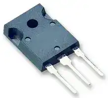
- Transistor Case Style: TO-247AC
- Operating Temperature Max: 150°C
- Continuous Collector Current: 75A
- Collector Emitter Voltage Max: 600V
- Collector Emitter Saturation Voltage: 3.2V
| Delivery and price | |
|---|---|
| Units per pack | 1 |
| Price | 2.38 € |
| Current stock | 10+ |
| Lead time | 30 days |
## IRGP50B60PDPbF

## **SMPS IGBT**

## WARP2 SERIES IGBT WITH ULTRAFAST SOFT RECOVERY DIODE

## **Applications**

- Telecom and Server SMPS

- PFC and ZVS SMPS Circuits

- Uninterruptable Power Supplies

- Consumer Electronics Power Supplies

- Lead- Free

## **Features**

**==> picture [80 x 115] intentionally omitted <==**

**----- Start of picture text -----**<br>
C<br>G<br>E<br>n-channel<br>**----- End of picture text -----**<br>


VCES = 600V VCE(on) typ. = 2.00V @ VGE = 15V IC = 33A

**Equivalent MOSFET Parameters** RCE(on) typ. = 61mΩ ID (FET equivalent) = 50A

- NPT Technology, Positive Temperature Coefficient

- Lower VCE(SAT)

- Lower Parasitic Capacitances

- Minimal Tail Current

- HEXFRED Ultra Fast Soft-Recovery Co-Pack Diode

- Tighter Distribution of Parameters

- Higher Reliability

## **Benefits**

- Parallel Operation for Higher Current Applications

**==> picture [56 x 51] intentionally omitted <==**

**----- Start of picture text -----**<br>
E<br>C<br>G<br>TO-247AC<br>**----- End of picture text -----**<br>


- Lower Conduction Losses and Switching Losses

- Higher Switching Frequency up to 150kHz

## **Absolute Maximum Ratings**

||**Parameter**|**Max.**|**Units**|
|---|---|---|---|
|VCES|Collector-to-Emitter Voltage<br>~~a~~|600<br>~~a~~|V<br>~~a~~|
|IC@ TC =25°C|Continuous CollectorCurrent<br>~~a~~<br>~~**a**~~|75<br>~~a~~<br>~~**a**~~|A<br>~~a~~<br>~~7~~|
|IC@ TC =100°C|Continuous CollectorCurrent<br>~~**a**~~|42<br>~~**a**~~||
|ICM|Pulse CollectorCurrent (Ref. Fig.C.T.4)<br>~~**a**~~|150<br>~~**a**~~||
|ILM|Clamped Inductive Load  Current<br>~~**a**~~<br>~~eee~~|150<br>~~**a**~~<br>~~eee~~||
|IF@ TC =25°C|Diode ContinousForward Current<br>~~**a**~~<br>~~ee~~|50<br>~~**a**~~<br>~~ee~~||
|IF@ TC =100°C|Diode ContinousForward Current<br>~~**a**~~<br>~~a~~|25<br>~~**a**~~<br>~~a~~||
|IFRM|Maximum Repetitive Forward Current<br>~~**a**~~|100<br>~~**a**~~||
|VGE|Gate-to-Emitter Voltage<br>~~ee~~|±20<br>~~ee~~|V|
|PD@ TC =25°C|Maximum Power Dissipation<br>~~ee~~|370<br>~~ee~~<br>~~SS~~|W<br>~~po~~|
|PD@ TC =100°C<br>~~po~~|Maximum Power Dissipation<br>~~eee~~<br>~~po~~|150<br>~~eee~~<br>~~po~~||
|TJ<br>TSTG<br>~~po~~|Operating Junction and<br>StorageTemperatureRange<br>~~eee~~<br>~~po~~|-55 to +150<br>~~eee~~<br>~~po~~|°C<br>~~po~~|
|~~po~~|SolderingTemperaturefor 10 sec.<br>~~po~~|300 (0.063in.(1.6mm)fromcase)<br>~~po~~||
|~~po~~|MountingTorque, 6-32or M3 Screw<br>~~po~~<br>~~a~~|10lbf·in(1.1 N·m)<br>~~po~~<br>~~a~~|~~po~~<br>~~a~~|


## **Thermal Resistance**

||**Parameter**|**Min.**|**Typ.**|**Max.**|**Units**|
|---|---|---|---|---|---|
|RθJC (IGBT)|Thermal Resistance Junction-to-Case-(each IGBT)|–––|–––|0.34|°C/W|
|RθJC (Diode)|Thermal Resistance Junction-to-Case-(each Diode)|–––|–––|0.64||
|RθCS|Thermal Resistance,Case-to-Sink(flat, greased surface)|–––|0.50|–––||
|RθJA|Thermal Resistance,Junction-to-Ambient(typical socket mount)|–––|–––|40||
||Weight|–––|6.0 (0.21)|–––|g (oz)|


www.irf.com

1

## IRGP50B60PDPbF

## **Electrical Characteristics @ TJ = 25°C (unless otherwise specified)**

|~~Ce~~|**Parameter**<br>~~Ce~~|**Min.**|**Typ.**|**Max. **|**Units **|**Conditions**|**Ref.Fig**|
|---|---|---|---|---|---|---|---|
|V(BR)CES<br>~~Ce~~|Collector-to-Emitter Breakdown Voltage<br>~~Ce~~|600|—<br>~~CO~~|—<br>~~CO~~|V|VGE= 0V, IC= 500µA||
|∆V(BR)CES/∆TJ<br>~~Ce~~|Temperature Coeff. of Breakdown Voltage<br>~~Ce~~<br>~~RD~~|—<br>~~RD~~|0.61<br>~~RD~~<br>~~CO~~<br>~~DD~~|—<br>~~RD~~<br>~~CO~~<br>~~DD~~|V/°C <br>~~RD~~<br>~~OO~~|VGE= 0V,IC= 1mA(25°C-125°C)<br>~~RD~~||
|RG<br>~~Ce~~|Internal Gate Resistance<br>~~Ce~~<br>~~RD~~<br>~~GD~~|—<br>~~RD~~<br>~~GD~~|1.2<br>~~RD~~<br>~~CO~~<br>~~GD~~<br>~~DD~~|—<br>~~RD~~<br>~~CO~~<br>~~GD~~<br>~~DD~~|Ω<br>~~RD~~<br>~~GD~~<br>~~OO~~|1MHz,Open Collector<br>~~RD~~<br>~~GD~~|~~GD~~|
|VCE(on)<br>~~Ne~~|Collector-to-Emitter Saturation Voltage<br>~~GD~~<br>~~Ne~~|—<br>~~GD~~|2.0<br>~~GD~~<br>~~DD~~<br>~~PT~~|2.2<br>~~GD~~<br>~~DD ~~<br>~~PT~~|V<br>~~GD~~<br> ~~OO~~<br>|IC= 33A,VGE= 15V<br>~~GD~~|4, 5,6,8,9<br>~~GD~~<br>|
|||—|2.4<br>~~PT~~|2.6<br>~~PT~~||IC= 50A, VGE= 15V||
|||—|2.6<br>~~TT~~|2.9<br>~~TT~~||IC= 33A,VGE= 15V,TJ= 125°C||
|||—<br>|3.2<br>~~PT~~<br>|3.6<br>~~PT~~<br>||IC= 50A, VGE= 15V, TJ= 125°C<br>||
|VGE(th)<br>~~Ne~~|Gate Threshold Voltage<br>~~Ne~~|3.0<br>~~A~~|4.0<br>~~PT~~<br>~~A~~<br>~~GO~~|5.0<br>~~PT~~<br>~~A~~<br>~~GO GO~~|V<br>~~A~~<br>~~GO~~|IC= 250µA<br>~~A~~<br>~~GO~~|7,8,9<br>~~A~~|
|∆VGE(th)/∆TJ<br>~~Ne~~|Threshold Voltage temp. coefficient<br>~~Ne ~~<br>~~GD~~|—<br> ~~A~~<br>~~GD~~|-7.07<br>~~PT~~<br>~~A~~<br>~~GD~~<br>~~GO~~|—<br>~~PT~~<br>~~A~~<br>~~GD~~<br>~~GO GO~~<br>~~OG~~|mV/°C <br>~~A~~<br>~~GD~~<br>~~GO~~<br>~~OG~~|VCE= VGE, IC= 1.0mA<br>~~A~~<br>~~GD~~<br>~~GO~~||
|gfe<br>~~Ne~~|Forward Transconductance<br>~~Ne ~~<br>~~GD~~|—<br> <br>~~GD~~|42<br>~~PT~~<br><br>~~GO~~<br>~~GD~~|—<br>~~PT~~<br><br>~~GO GO~~<br>~~GD~~<br>~~OG~~|S<br><br>~~GO~~<br>~~GD~~<br>~~OG~~|VCE= 50V,IC= 33A,PW = 80µs<br><br>~~GO~~<br>~~GD~~|~~GD~~|
|ICES|Collector-to-Emitter Leakage Current<br>~~EEE~~|—<br>~~EEE~~|5.0<br>~~EEE~~|500<br>~~OG~~<br>~~EEE~~|µA<br>~~OG~~<br>~~EEE~~|VGE= 0V, VCE= 600V<br>~~EEE~~|~~EEE~~|
|||—<br>~~EEE~~|1.0<br>~~EEE~~<br>~~a~~|—<br>~~EEE~~<br>~~ee~~|mA<br>~~EEE~~<br>~~ee~~|VGE= 0V,VCE= 600V,TJ= 125°C<br>~~EEE~~||
|VFM|Diode Forward Voltage Drop<br>~~EEE~~|—<br>~~EEE~~|1.3<br>~~EEE~~<br>~~a~~<br>~~PT~~|1.7<br>~~EEE~~<br>~~ee~~<br>~~PT~~|V<br>~~EEE~~<br>~~ee~~|IF= 25A, VGE= 0V<br>~~EEE~~|10<br>~~EEE~~|
|||—|1.5<br>~~PT~~|2.0<br>~~PT~~||IF= 50A,VGE= 0V||
|||—|1.3<br>~~PT~~|1.7<br>~~PT~~||IF= 25A,  VGE= 0V, TJ= 125°C||
|IGES|Gate-to-Emitter Leakage Current<br>~~GG~~|—<br>~~GG~~|—<br>~~PT~~<br>~~GG~~|±100<br>~~PT~~<br>~~GG~~|nA<br>~~GG~~|VGE= ±20V,VCE= 0V<br>~~GG~~|~~GG~~|


## **Switching Characteristics @ TJ = 25°C (unless otherwise specified)**

|~~PC~~|**Parameter**<br>~~PC~~|**Min.**<br>|**Typ.**<br>|**Max. **<br>|**Units**|**Conditions**|**Ref.Fig**|
|---|---|---|---|---|---|---|---|
|Qg<br>~~PC~~|Total Gate Charge(turn-on)<br>~~PCr—“COOTTTTTTCti‘*dESC~~|—<br>~~r—“COOTTTTTTCti‘*dESC~~|240<br>~~r—“COOTTTTTTCti‘*dESC~~|360<br>~~r—“COOTTTTTTCti‘*dESC~~|nC|IC= 33A<br>VCC= 400V<br>VGE= 15V|17<br>CT1|
|Qgc<br>~~PC~~|Gate-to-Collector Charge(turn-on)<br>~~PC~~<br>~~a~~|—<br><br>~~a~~|41<br><br>~~a~~|82<br><br>~~a~~||||
|Qge<br>~~a~~|Gate-to-Emitter Charge(turn-on)<br>~~a~~<br>~~a~~|—<br>~~a~~|84<br>~~a~~|130<br>~~a~~||||
|Eon<br>~~a~~<br>~~PC~~|Turn-On SwitchingLoss<br>~~a~~<br>~~a~~<br>~~PC~~|—<br>~~a~~<br>|360<br>~~a~~<br>|590<br>~~a~~<br>|µJ|IC= 33A, VCC= 390V<br>VGE= +15V, RG= 3.3Ω, L = 210µH<br>TJ = 25°C<br>@|CT3|
|Eoff<br>~~a~~<br>~~PC~~|Turn-Off SwitchingLoss<br>~~a~~<br>~~PCr—“COOTTTTTTCti‘*dESC~~|—<br>~~r—“COOTTTTTTCti‘*dESC~~|380<br>~~r—“COOTTTTTTCti‘*dESC~~|420<br>~~r—“COOTTTTTTCti‘*dESC~~||||
|Etotal<br>~~PC~~<br>~~PC~~|Total SwitchingLoss<br>~~PC~~<br>~~a~~<br>~~PC~~|—<br><br>|740<br><br>|960<br><br>||||
|td(on)<br>~~PC~~|Turn-On delaytime<br>~~PCr—“COOTTTTTTCti‘*dESC~~|—<br>~~r—“COOTTTTTTCti‘*dESC~~|34<br>~~r—“COOTTTTTTCti‘*dESC~~|44<br>~~r—“COOTTTTTTCti‘*dESC~~|I<br>ns|IC= 33A, VCC= 390V<br>VGE= +15V, RG= 3.3Ω, L = 210µH<br>TJ= 25°C<br>co)|CT3|
|tr<br>~~PC~~<br>~~PC~~|Rise time<br>~~PC~~<br>~~a~~<br>~~PC~~<br>~~r—“COOTTTTTTCti‘*dESC~~|—<br><br>~~a~~<br>~~r—“COOTTTTTTCti‘*dESC~~|26<br><br>~~a~~|36<br><br>~~a~~||||
|td(off)<br>~~PC~~|Turn-Off delaytime<br>~~PC~~<br>~~r—“COOTTTTTTCti‘*dESC~~|—<br>~~r—“COOTTTTTTCti‘*dESC~~|130|140||||
|tf<br>~~PC~~<br>~~PC~~|Fall time<br>~~PC~~<br>~~r—“COOTTTTTTCti‘*dESC~~<br>~~a~~<br>~~PC~~|—<br>~~r—“COOTTTTTTCti‘*dESC~~<br>~~a~~<br>|43<br>~~a~~<br>|56<br>~~a~~<br>||||
|Eon<br>~~PC~~|Turn-On SwitchingLoss<br>~~PCr—“COOTTTTTTCti‘*dESC~~|—<br>~~r—“COOTTTTTTCti‘*dESC~~|610<br>~~r—“COOTTTTTTCti‘*dESC~~|880<br>~~r—“COOTTTTTTCti‘*dESC~~|I<br>µJ|IC= 33A, VCC= 390V<br>VGE= +15V, RG= 3.3Ω, L = 210µH<br>TJ= 125°C<br>®|CT3<br>11,13<br>WF1,WF2|
|Eoff<br>~~PC~~|Turn-Off SwitchingLoss<br>~~PC~~<br>~~a~~|—<br><br>~~a~~|460<br><br>~~a~~|530<br><br>~~a~~||||
|Etotal<br>~~a~~|Total SwitchingLoss<br>~~a~~<br>~~a~~|—<br>~~a~~|1070<br>~~a~~|1410<br>~~a~~||||
|td(on)<br>~~a~~<br>~~PC~~|Turn-On delaytime<br>~~a~~<br>~~a~~<br>~~PC~~|—<br>~~a~~<br>|33<br>~~a~~<br>|43<br>~~a~~<br>|I<br>ns|IC= 33A, VCC= 390V<br>VGE= +15V, RG= 3.3Ω, L = 200µH<br>TJ= 125°C<br>®|CT3<br>12,14<br>WF1,WF2|
|tr<br>~~a~~<br>~~PC~~|Rise time<br>~~a~~<br>~~PCr—“COOTTTTTTCti‘*dESC~~|—<br>~~r—“COOTTTTTTCti‘*dESC~~|26<br>~~r—“COOTTTTTTCti‘*dESC~~|36<br>~~r—“COOTTTTTTCti‘*dESC~~||||
|td(off)<br>~~PC~~<br>~~PC~~|Turn-Off delaytime<br>~~PC~~<br>~~a~~<br>~~PC~~|—<br><br>|140<br><br>|160<br><br>||||
|tf<br>~~PC~~|Fall time<br>~~PCr—“COOTTTTTTCti‘*dESC~~|—<br>~~r—“COOTTTTTTCti‘*dESC~~|50<br>~~r—“COOTTTTTTCti‘*dESC~~|65<br>~~r—“COOTTTTTTCti‘*dESC~~||||
|Cies<br>~~PC~~<br>~~PC~~|Input Capacitance<br>~~PC~~<br>~~a~~<br>~~PC~~|—<br><br>~~a~~<br>|4750<br><br>~~a~~<br>|—<br><br>~~a~~<br>|pF|VGE= 0V<br>VCC= 30V<br>f = 1Mhz|16|
|Coes<br>~~PC~~|Output Capacitance<br>~~PC—(CsTTTTT.TCSS~~|—<br>~~—(CsTTTTT.TCSS~~|390<br>~~—(CsTTTTT.TCSS~~|—<br>~~—(CsTTTTT.TCSS~~||||
|Cres<br>~~PC~~|Reverse Transfer Capacitance<br>~~PC~~<br>~~a~~|—<br><br>~~a~~|58<br><br>~~a~~|—<br><br>~~a~~||||
|Coeseff.|Effective Output Capacitance (Time Related)<br>~~Se~~|—|280|—||VGE= 0V, VCE= 0V to 480V|15<br>~~|~~|
|Coeseff.(ER)|Effective Output Capacitance (Energy Related)<br>~~Se~~|—|190|—||||
|RBSOA|Reverse Bias Safe Operating Area<br>~~Se~~|FULL SQUARE<br>~~eS~~|||~~eS~~<br>~~LE~~|TJ= 150°C, IC= 150A<br>VCC= 480V, Vp =600V<br>Rg= 22Ω,VGE= +15V to 0V<br>~~LE~~<br>~~sd~~|3<br>CT2<br>~~|~~<br>~~sd~~|
|trr|Diode Reverse Recovery Time<br>~~PE~~|—<br>~~PE~~<br>~~eS~~|50<br>~~PE~~<br>~~eS~~|75<br>~~PE~~<br>~~eS~~|ns<br>~~PE~~<br>~~eS~~<br>~~LE~~|TJ= 25°C<br>IF= 25A, VR= 200V,<br>TJ= 125°C<br>di/dt = 200A/µs<br>~~PE~~<br>~~LE~~<br>~~sd~~|19<br>~~PE~~<br>~~sd~~|
|||—<br>~~PE~~<br>~~eS~~|105<br>~~PE~~<br>~~eS~~|160<br>~~PE~~<br>~~eS~~||||
|Qrr<br>~~po~~|Diode Reverse Recovery Charge<br>~~es~~<br>~~po~~|—<br>~~eS~~<br>~~es~~|112<br>~~eS~~<br>~~es~~|375<br>~~eS~~<br>~~es~~|nC<br>~~eS~~<br>~~LE~~<br>~~es~~<br>~~PE~~|TJ= 25°C<br>IF= 25A, VR= 200V,<br>TJ= 125°C<br>di/dt = 200A/µs<br>~~LE~~<br>~~sd~~<br>~~es~~<br>~~PE~~|21<br>~~sd~~<br>~~es~~<br>~~PE~~|
|||—<br>~~es~~|420<br>~~es~~<br>~~PT~~|4200<br>~~es~~<br>~~PT~~||||
|~~Notes:~~<br>Irr<br>~~po~~|Peak Reverse Recovery Current<br>~~es~~<br>~~po~~|—<br>~~es~~|4.5<br>~~es~~<br>~~PT~~|10<br>~~es~~<br>~~PT~~|A<br>~~es~~<br>~~PE~~|TJ= 25°C<br>IF= 25A, VR= 200V,<br>TJ= 125°C<br>di/dt = 200A/µs<br>~~es~~<br>~~PE~~|19,20,21,22<br>CT5<br>~~es~~<br>~~PE~~|
|||—|8.0<br>~~PT~~<br>~~TT~~|15<br>~~PT~~<br>~~TT~~||||


~~Notes:~~

® RCE(on) typ. = equivalent on-resistance = VCE(on) typ./ IC, where VCE(on) typ.= 2.00V and IC =33A. ID (FET Equivalent) is the equivalent MOSFET ID rating @ 25°C for applications up to 150kHz. These are provided for comparison purposes (only) with equivalent MOSFET solutions. oO) VCC = 80% (VCES), VGE = 20V, L = 28 µH, RG = 22 Ω.

Pulse width limited by max. junction temperature.

Energy losses include "tail" and diode reverse recovery, Data generated with use of Diode 30ETH06.

Coes eff. is a fixed capacitance that gives the same charging time as Coes while VCE is rising from 0 to 80% VCES.

Coes eff.(ER) is a fixed capacitance that stores the same energy as Coes while VCE is rising from 0 to 80% VCES.

www.irf.com

2

IRGP50B60PDPbF

**==> picture [207 x 671] intentionally omitted <==**

**----- Start of picture text -----**<br>
80<br>70 Limited by package<br>60 S S<br>a N |<br>50 P oE NK Ef<br>40 P ot EN |<br>30 N e<br>20 P ot<br>10 P f fF EK<br>0 | | fltf EENtf<br>25 50 75 100 125 150<br> TC, Case Temperature (°C)<br>Fig. 1  - Maximum DC Collector Current vs.<br>Case Temperature<br>1000<br>PTE ath<br>100<br>10<br>H H<br>1 el<br>10 100 1000<br>VCE (V)<br>Fig. 3  - Reverse Bias SOA<br>TJ = 150°C; VGE =15V<br>320<br>280 V  = 15V<br>GE Arm<br>VGE = 12V<br>240<br>VGE = 10V<br>VGE = 8.0V<br>200 VGE = 6.0V<br>~/a<br>160<br>a TAL |<br>120<br>P P OCa<br>80<br>ee<br>40<br>n y)<br>0 | A Ae| IN<br>0 2 4 6 8 10<br> VCE (V)<br>IC, Collector Current (A)<br>ICE (A)<br>IC A)<br>**----- End of picture text -----**<br>


**==> picture [205 x 194] intentionally omitted <==**

**----- Start of picture text -----**<br>
400<br>350<br>300 a l | tt tt<br>P EN EL |<br>250 P T IN | |fd<br>200 P TT<br>P ett<br>150 IN | td<br>100 | INE Et<br>50 E ReeeNee<br>0 SPtatTeeeeNett te LK<br>0 20 40 60 80 100 120 140 160<br> TC (°C)<br>Ptot (W)<br>**----- End of picture text -----**<br>


**Fig. 2** - Power  Dissipation vs. Case Temperature

**==> picture [201 x 194] intentionally omitted <==**

**----- Start of picture text -----**<br>
320<br>280 V  = 15V<br>GE<br>VGE = 12V<br>240 V/i| |<br>VGE = 10V<br>VGE = 8.0V<br>200 VGE = 6.0V<br>160<br>120<br>80<br>40 / |<br>0 PZ NT<br>0 2 4 6 8 10<br> VCE (V)<br>ICE (A)<br>**----- End of picture text -----**<br>


**Fig. 4** - Typ. IGBT Output Characteristics TJ = -40°C; tp = 80µs

**==> picture [201 x 193] intentionally omitted <==**

**----- Start of picture text -----**<br>
320<br>280 VGE = 15V<br>VGE = 12V ae/SGnn<br>VGE = 10V<br>240<br>VGE = 8.0V<br>VGE = 6.0V<br>200<br>e o<br>160<br>E D) SNEee e<br>120<br>S ay AGRGn e<br>80<br>E e)<br>40<br>Ga N<br>0 XIALELL E LLLLL<br>0 2 4 6 8 10 12 14 16 18 20<br> VCE (V)<br>ICE (A)<br>**----- End of picture text -----**<br>


**Fig. 5** - Typ. IGBT Output Characteristics TJ = 25°C; tp = 80µs

**Fig. 6** - Typ. IGBT Output Characteristics TJ = 125°C; tp = 80µs

www.irf.com

3

## IRGP50B60PDPbF

**==> picture [205 x 194] intentionally omitted <==**

**----- Start of picture text -----**<br>
600<br>TJ = 25°C<br>500 TJ = 125°C<br>| ff<br>400<br>P | lt<br>300<br>| | Ff | |<br>200<br>TJ = 125°C<br>100 P y f | |<br>T  = 25°C<br>J<br>0 | Yr |<br>0 5 10 15 20<br> VGE (V)<br>ICE (A)<br>**----- End of picture text -----**<br>


**Fig. 7** - Typ. Transfer Characteristics VCE = 50V; tp = 10µs

**==> picture [195 x 194] intentionally omitted <==**

**----- Start of picture text -----**<br>
25<br>20<br>a ta<br>a ie<br>15 I  = 15A<br>CE<br>I = 33A<br>CE<br>10 m ie ICE = 50A<br>5<br>i aae<br>0 (eee<br>0 5 10 15 20<br> VGE (V)<br>VCE (V)<br>**----- End of picture text -----**<br>


**Fig. 8** - Typical VCE vs. VGE TJ = 25°C

**==> picture [464 x 433] intentionally omitted <==**

**----- Start of picture text -----**<br>
25 100<br>20<br>T  = 150°CJ<br>15 | eee ebL |,A T  = 125°CJ<br>ICE = 15A T  =   25°CJ<br>I = 33A 10<br>CE<br>10 ICE = 50A<br>1 © EY<br>5<br>0 SS TEL 1 LL<br>0.6 1.0 1.4 1.8 2.2 2.6<br>0 5 10 15 20  Forward Voltage Drop - V      (V)FM<br> VGE (V)<br>Fig. 9  - Typical VCE vs. VGE Fig. 10  - Maximum. Diode Forward<br>TJ = 125°C Characteristics tp = 80µs<br>1800 1000<br>1600<br>E<br>1400 ASCO ON T<br>1200 a PE LT EE ye<br>td<br>OFF<br>1000 EOFF 100<br>E y I | tF p<br>800<br>600 td<br>ON<br>400 tR<br>200 eZee 10 H-ARTEEE<br>10 20 30 40 50 60 70 0 10 20 30 40 50 60 70<br> IC (A) IC (A)<br>VCE (V)<br>Energy (µJ)<br>Swiching Time (ns)<br>**----- End of picture text -----**<br>


**Fig. 11** - Typ. Energy Loss vs. IC TJ = 125°C; L = 200µH; VCE = 390V, RG = 3.3Ω; VGE = 15V. Diode clamp used: 30ETH06 (See C.T.3)

**Fig. 12** - Typ. Switching Time vs. IC TJ = 125°C; L = 200µH; VCE = 390V, RG = 3.3Ω; VGE = 15V. Diode clamp used: 30ETH06 (See C.T.3)

www.irf.com

4

IRGP50B60PDPbF

**==> picture [455 x 195] intentionally omitted <==**

**----- Start of picture text -----**<br>
1800 1000<br>1600 EOFF<br>1400 | | P| es tdOFF de<br>a n aa a<br>1200<br>1000 r T [7 |_. 100 4 m<br>800 tF<br>E<br>ON<br>600 eae — tdON<br>tR<br>400<br>200 7e 7e|.ee  | 10 Caay pn<br>0 10 20 30 40 0 10 20 30 40<br>RG (Ω) RG (Ω)<br>Energy (µJ)<br>Swiching Time (ns)<br>**----- End of picture text -----**<br>


**Fig. 13** - Typ. Energy Loss vs. RG

TJ = 125°C; L = 200µH; VCE = 390V, ICE = 33A; VGE = 15V Diode clamp used: 30ETH06 (See C.T.3)

**==> picture [197 x 197] intentionally omitted <==**

**----- Start of picture text -----**<br>
35<br>30<br>25 r TTY|<br>20<br>15 p o fe<br>10 S ap 4500<br>5 D 2<br>0 Zannnnn<br>0 100 200 300 400 500 600 700<br>Voltage (V)<br>Eoes (µJ)<br>**----- End of picture text -----**<br>


**Fig. 15** - Typ. Output Capacitance Stored Energy vs. VCE

**Fig. 14** - Typ. Switching Time vs. RG TJ = 125°C; L = 200µH; VCE = 390V, ICE = 33A; VGE = 15V Diode clamp used: 30ETH06 (See C.T.3)

**==> picture [200 x 221] intentionally omitted <==**

**----- Start of picture text -----**<br>
10000<br>Cies<br>| eeee ee<br>FR EE<br>1000<br>AN Coes eeeee eee<br>L a<br>100 a<br>Cres<br>~— —<br>_<br>10<br>0 100 200 300 400 500<br>VCE (V)<br>Fig. 16 - Typ. Capacitance vs. VCE<br> VGE= 0V; f = 1MHz<br>Capacitance (pF)<br>**----- End of picture text -----**<br>


**==> picture [200 x 191] intentionally omitted <==**

**----- Start of picture text -----**<br>
16<br>14<br>V  = 480V<br>CE<br>an<br>12 m a aa n<br>10<br>8 Hn nnERATane<br>6<br>4 Fv ERCir<br>2<br>0 P REC re  EE<br>0 50 100 150 200 250 300<br>Q G, Total Gate Charge (nC)<br>VGE, Gate-to-Emitter Voltage (V)<br>**----- End of picture text -----**<br>


**Fig. 17** - Typical Gate Charge vs. VGE ICE = 33A

**==> picture [198 x 194] intentionally omitted <==**

**----- Start of picture text -----**<br>
1.5<br>LLL ELLE<br>1.3 iL<br>1.0 a tlpzd<br>0.8 A LTLLLEELLLL ELL<br>0.5<br>-60 -40 -20 0 20 40 60 80 100 120 140 160<br>TC (°C)<br>Normalized VCE(on)<br>**----- End of picture text -----**<br>


**Fig. 18** - Normalized Typ. VCE(on) vs. Junction Temperature IC = 33A, VGE= 15V

www.irf.com

5

IRGP50B60PDPbF

**==> picture [201 x 239] intentionally omitted <==**

**----- Start of picture text -----**<br>
140<br>V  = 200VR<br>T  = 125°CJ<br>T  = 25°CJ<br>LJ<br>120<br>tL =]<br>100 Po<br>Zz<br>_ ee<br>I   = 50AF<br>S 80 P| a<br>I   = 25AF<br>: pss, ts<br>CATT<br>I   = 10AF<br>60<br>PSE<br>SS<br>40 ee aes<br>PSPT<br>20<br>100 1000<br>di  /dt - (A/µs)f<br>**----- End of picture text -----**<br>


**==> picture [199 x 243] intentionally omitted <==**

**----- Start of picture text -----**<br>
30<br>V  = 200VR<br>T  = 125°CJ<br>T  = 25°CJ<br>25<br>CT [=F]<br>20 p I   = 50AF o e<br>I   = 25AF<br>pe<br>I   = 10AF<br>- 15 See,<br>es ede p<br>9/74<br>10 gy<br>|<br>Yaa<br>5 Qo<br>asee e n<br>0<br>100 1000<br>di  /dt - (A/µs)f<br>**----- End of picture text -----**<br>


**==> picture [468 x 238] intentionally omitted <==**

**----- Start of picture text -----**<br>
1400 10000<br>V  = 200VR V  = 200VR<br>T  = 125°CJ LEE T  = 125°CJ 7<br>1200 |= T  = 25°CJ T  = 25°CJ nnn<br>1000 a re  t o e t aaod |rra =ee Feeee e<br>I   = 50AF<br>SE ee ee<br>I   = 25AF<br>800<br>I   F = 10A I   = 50AF<br>1000<br>600 I   = 25AF<br>I   = 10AF<br>400 aeCoaneTSA Aa | : aeSLEaaagE<br>200 oe | Site Bail<br>A<br>0 ees ed 100 gone"<br>100 1000 100 1000<br>di  /dt - (A/µs)f di  /dt - (A/µs)f<br>**----- End of picture text -----**<br>


www.irf.com

6

IRGP50B60PDPbF

**==> picture [436 x 694] intentionally omitted <==**

**----- Start of picture text -----**<br>
1<br>pot PT teapetatmensensncreomentse-rennrentmoperat<br>D = 0.50<br>Se te m tt tH<br>0.1 Pe ao<br>— 0.20 SS ne n e I eee<br>sm 0 .10 m rt m<br>0.01 _— |e e 0.050.02 Spm at e τJ τJ t R L 1 R1 R2 R2 τCτ e Ri (°C/W)   0.0789     0.000277 τi (sec) llHA<br>TE—"| 0.01 a eeeAZa eee eee τ1 τ1 τ2τ2 0.2614     0.040918 HHani<br>ee eee eee Ci=  T Ciτi/Rii/Ri T rd LL]<br>0.001 | | SINGLE PULSE Ue<br>= aeer ( THERMAL RESPONSE ) EEA HS Notes:<br>iA | | Py EEE MaanEHH<br>1. Duty Factor D = t1/t2<br>2. Peak Tj = P dm x Zthjc + Tc<br>ee i<br>0.0001<br>1E-006 1E-005 0.0001 0.001 0.01 0.1 1<br>t1 , Rectangular Pulse Duration (sec)<br>Fig 23.   Maximum Transient Thermal Impedance, Junction-to-Case (IGBT)<br>1<br>FT Te T T ar aaaaa gn nalenntantane=tetey—esoneentanessataasstenstentshetets<br>D = 0.50<br>me TH TTT<br>0.1 fmm A 0 ec |<br>0.20<br>iz, a e e a ee<br>—— 0.10 ee ee ee ee eee<br>0.01 | =Pr z | 0.050.02 SSpnC Tteo—|art τJ τ p J R1 R pg 1 R2 R2 R3R3 τCτ |ee Ri (°C/W)   0.0733     0.000420 τi (sec)  el<br>= 0.01 e T eeAa ane τ1τ LL 1 LL τ2 τ2 iL τ3τ3 0.1301     0.002274 FY]HH<br>ci eee ee T T T IL<br>p H Ci= Ciτi/Rii/Ri | 0.1358     0.023026 LT<br>0.001 ea ET eee | ee<br>iP | SINGLE PULSE re ee Notes: 2 ee ee ee<br>( THERMAL RESPONSE ) 1. Duty Factor D = t1/t2<br>Cac reeeis ec eri meal<br>2. Peak Tj = P dm x Zthjc + Tc<br>A it EA a<br>0.0001<br>1E-006 1E-005 0.0001 0.001 0.01 0.1 1<br>t1 , Rectangular Pulse Duration (sec)<br>Fig. 24.   Maximum Transient Thermal Impedance, Junction-to-Case (DIODE)<br>1000<br>OPERATION IN THIS AREA<br>4a LIMITED BY V CE(on) TT TTT<br>a Ae eee ee e e<br>100 a, F RE EF SAEE<br>100µsec<br>a eee, e ee ee<br>1 m sec<br>10 pTH oe Ny st tth e T OR TI<br>10msec<br>a a ee ee e e ee ee e<br>Pa] | tyS g<br>1 e s “ COT<br>100msec<br>a e e<br>0.1 A<br>Tc = 25°C<br>Tj = 150°C<br>reee e ee Sl<br>Single Pulse<br>e e<br>0.01<br>1 10 100 1000<br>VDS, Drain-to-Source Voltage (V)<br>ID,  Drain-to-Source Current (A)<br>Thermal Response ( Z thJC )<br>Thermal Response ( Z thJC )<br>**----- End of picture text -----**<br>


**Fig. 25** - Forward SOA, TC = 25°C; TJ ≤ 150°C

www.irf.com

7

IRGP50B60PDPbF

**==> picture [436 x 92] intentionally omitted <==**

**----- Start of picture text -----**<br>
L<br>L<br>VCC<br>DUT 80 V DUT<br>0 480V<br>1K Rg<br>**----- End of picture text -----**<br>


**Fig.C.T.1** - Gate Charge Circuit (turn-off)

**Fig.C.T.2** - RBSOA Circuit

**==> picture [448 x 97] intentionally omitted <==**

**----- Start of picture text -----**<br>
VCC<br>PFC diode L R =<br>ICM<br>DUT /<br>VCC<br>DRIVER DUT VCC<br>Rg<br>Rg<br>**----- End of picture text -----**<br>


**Fig.C.T.3** - Switching Loss Circuit

**Fig.C.T.4** - Resistive Load Circuit

## REVERSE RECOVERY CIRCUIT

**==> picture [105 x 100] intentionally omitted <==**

**----- Start of picture text -----**<br>
V    = 200VR<br>0.01 Ω<br>L = 70µH<br>D.U.T.<br>D<br>  dif/dt<br>ADJUST G IRFP250<br>S<br>**----- End of picture text -----**<br>


**Fig. C.T.5** - Reverse Recovery Parameter Test Circuit

www.irf.com

8

IRGP50B60PDPbF

**==> picture [219 x 233] intentionally omitted <==**

**----- Start of picture text -----**<br>
700 35<br>tf<br>600 aa - 30<br>Vce<br>500 25<br>90% Ice<br>400 20<br>300 15<br>Ice<br>5% Vce<br>200 10<br>5% Ice<br>100 5<br>0 yA> Saas 0<br>KA |<br>r Eoff Loss |<br>|<—— — |<br>-100 -5<br>-0.05 0 0.05 0.1 0.15<br>Time (uS)<br>Vce (V) Ice (A)<br>**----- End of picture text -----**<br>


**Fig. WF1** - Typ. Turn-off Loss Waveform @ TJ = 25°C using Fig. CT.3

**==> picture [206 x 233] intentionally omitted <==**

**----- Start of picture text -----**<br>
700 70<br>—- 1 tr /<br>600 | | =_ch- 60<br>Ice<br>Vce<br>500 50<br>90% Ice<br>400 40<br>300 30<br>10% Ice<br>5% Vce<br>200 20<br>100 10<br>0 NS VRe KPe 0<br>Eon |<br>—_ | Loss |—| —<br>-100 -10<br>3.95 4.05 4.15 4.25<br>Time (uS)<br>Vce (V) Ice (A)<br>**----- End of picture text -----**<br>


**Fig. WF2** - Typ. Turn-on Loss Waveform @ TJ = 25°C using Fig. CT.3

**==> picture [312 x 140] intentionally omitted <==**

**----- Start of picture text -----**<br>
3<br>IF trr<br>ta tb<br>0<br>:H<br>: :: y“4 4<br>Q rr<br> \O:: 2 I RRM ’; 0.5 I RRM<br>H: 2<br>: ‘ ¢ di(rec)M/dt 5<br>0.75 IRRM<br>1 di  /dtf<br>**----- End of picture text -----**<br>


**Fig. WF3** - Reverse Recovery Waveform and Definitions

www.irf.com

9

## IRGP50B60PDPbF

Dimensions are shown in millimeters (inches)

**==> picture [410 x 99] intentionally omitted <==**

**----- Start of picture text -----**<br>
EXAMPLE: THIS IS AN IRFPE30<br>WITH ASSEMBLY  PART NUMBER<br>LOT CODE 5657 INTERNATIONAL<br>ASSEMBLED ON WW 35, 2000 RECTIFIER IRFPE30<br>LOGO  035H<br>IN THE ASSEMBLY LINE "H"<br>56           57<br>Note:   "P" in assembly line a DATE CODE<br>position indicates "Lead-Free" ASSEMBLY YEAR 0 =  2000<br>LOT CODE WEEK 35<br>LINE H<br>**----- End of picture text -----**<br>


## **TO-247AC package is not recommended for Surface Mount Application.**

Data and specifications subject to change without notice. This product has been designed and qualified for Industrial market. Qualification Standards can be found on IR’s Web site.

**IR WORLD HEADQUARTERS:** 233 Kansas St., El Segundo, California 90245, USA Tel: (310) 252-7105 TAC Fax: (310) 252-7903 Visit us at www.irf.com for sales contact information **.** 12/04

www.irf.com

10

Note:  For the most current drawings please refer to the IR website at: http://www.irf.com/package/
Updated at February 9, 2023
Infineon Technologies is a globally recognized leader in semiconductor solutions, renowned for driving innovation in power management, energy efficiency, and modern mobility. With a strong legacy of engineering excellence, the company provides highly reliable components designed to meet the rigorous demands of industrial, automotive, and advanced commercial applications. The core of our Infineon portfolio is centered on their industry-leading discrete semiconductors. We offer an extensive selection of single and dual MOSFETs, alongside a robust range of single IGBTs and advanced IGBT modules. These flagship power transistors are essential for high-efficiency power conversion and motor control, providing engineers with superior thermal performance and minimized switching losses. Beyond advanced field-effect transistors, the selection includes a comprehensive array of diodes and rectifiers, heavily featuring Schottky diodes, as well as fast-recovery and RF/PIN diodes. This power foundation is further supported by bipolar transistors, intelligent power modules, and thyristor SCR modules, delivering the critical building blocks required for complex power system designs. To support broader system integration, the portfolio also encompasses specialized solutions such as solid-state relays, AC/DC LED driver ICs, and Bluetooth communications modules. From high-power industrial rectifiers to wireless connectivity adapters, Infineon equips designers with the precision components needed to build efficient, scalable, and fully connected electronic systems.
About Novapart
Novapart is a B2B electronic component broker specialising in stock shortages and cost reduction. We source hard-to-find parts and identify compliant alternatives across a catalogue of 410,000+ components from 500+ manufacturers.
Learn more →Stock Shortage Specialist
When a component is unavailable, discontinued or has an unacceptable lead time, we tap into our network of vetted European and Asian distributors to source what you need — without compromising on quality or traceability.
Request a quote →Compliant Alternatives
We identify pin-to-pin, electrically equivalent substitutes that meet the same certifications (RoHS, AEC-Q100, REACH) as your original specification — validated against datasheets, not just part numbers. Often at a lower cost.
BOM Analysis service →