


IRGP4630DPBF
IGBT, 47 A, 1.65 V, 206 W, 600 V, TO-247AC, 3 Pins
- Manufacturer: INFINEON
- Product type: Single IGBTs
- DC Collector Current:47A; Collector Emitter Saturation Voltage Vce(on):1.65V; Power Dissipation Pd:206W; Collector Emitter Voltage V(br)ceo:600V; Transistor Case Style:TO-247AC; No. of Pins:3
- No. of Pins: 3Pins
- Product Range: -
- Power Dissipation: 206W
- Transistor Mounting: Through Hole
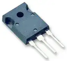
- Transistor Case Style: TO-247AC
- Operating Temperature Max: 175°C
- Continuous Collector Current: 47A
- Collector Emitter Voltage Max: 600V
- Collector Emitter Saturation Voltage: 1.65V
| Delivery and price | |
|---|---|
| Units per pack | 2500 |
| Price | 1.34 € |
| Current stock | 10+ |
| Lead time | 30 days |
IRGS4630DPbF IRGB4630DPbF IRGP4630D(-E)PbF ~~a~~ ## _**Insulated Gate Bipolar Transistor with Ultrafast Soft Recovery Diode**_ **==> picture [532 x 133] intentionally omitted <==** **----- Start of picture text -----**<br> VCES = 600V C<br>C C C C<br>IC = 30A, TC =100°C<br>G E E<br>tSC ≥ 5µs, TJ(max) = 175°C G C NR G C SNS G C [E ] G C [E ]<br>E<br>VCE(ON) typ. = 1.65V @ IC = 18A n-channel IRGS4630DPbF D [2] Pak IRGB4630DPbF TO-220AC IRGP4630DPbF TO-247AC IRGP4630D-EPbF TO-247AD<br>Applications G C E<br>Appliance Drives Gate Collector Emitter<br>**----- End of picture text -----**<br> ## **Applications** - Appliance Drives - Inverters - UPS ## **Features** ## **Benefits** Low VCE(ON) and switching losses High efficiency in a wide range of applications and switching Improved reliability due to rugged hard switching Square RBSOA and maximum junction temperature 175°C ~~ee~~ performance and high power capability Positive VCE (ON) temperature coefficient and tight distribution Excellent current sharing in parallel operation of parameters ~~a ee RC~~ 5µs Short Circuit SOA Enables short circuit protection scheme ~~eee~~ Lead-Free, RoHS Compliant Environmentally friendly |**Base part number**|**Package Type**|**Standard Pack**|**Standard Pack**|**Orderable Part Number**| |---|---|---|---|---| |||**Form**|**Quantity**|| |IRGS4630DPbF|D2Pak|Tube|50|IRGS4630DPbF| |||Tape and Reel Right|800|IRGS4630DTRRPbF| |||Tape and Reel Left|800|IRGS4630DTRLPbF| |IRGB4630DPbF|TO-220AB|Tube|50|IRGB4630DPbF| |IRGP4630DPbF|TO-247AC|Tube|25|IRGP4630DPbF| |IRGP4630D-EPbF|TO-247AD|Tube|25|IRGP4630D-EPbF| **Absolute Maximum Ratings** |~~a~~|**Parameter**<br>|**Max.**<br>|**Units**<br>| |---|---|---|---| |VCES<br>~~aDG~~<br>~~=SSS~~|Collector-to-Emitter Voltage<br>~~DG~~<br>~~=SSS~~|600<br>~~DG~~<br>~~=SSS~~|V<br>~~DG~~<br>~~I~~| |IC @TC= 25°C<br>~~=SSS~~<br>~~RC~~|Continuous Collector Current<br>~~=SSS~~|47<br>~~=SSS~~|A<br>~~I~~| |IC@ TC =100°C<br>~~=SSS~~<br>~~RC~~<br>~~RC~~|Continuous Collector Current<br>~~=SSS~~|30<br>~~=SSS~~|| |ICM<br>~~=SSS~~<br>~~RC~~<br>~~RC~~|Pulse Collector Current, VGE=15V<br>~~=SSS~~|54<br>~~=SSS~~|| |ILM<br>~~=SSS~~<br>~~RCa~~<br>~~PC~~|Clamped Inductive Load Current, VGE=20V<br>~~=SSS~~|72<br>~~=SSS~~|| |IF @TC= 25°C<br>~~=SSS~~<br>~~PCes~~|Diode Continuous Forward Current<br>~~=SSS~~|30<br>~~=SSS~~|| |IF @TC= 100°C<br>~~=SSS~~<br>~~PCes~~<br>~~i~~|Diode Continuous Forward Current<br>~~=SSS~~|18<br>~~=SSS~~<br>~~(~~|| |IFM<br>~~=SSS~~<br>~~es~~<br>~~nn~~<br>~~i~~|Diode Maximum Forward Current<br>~~=SSS~~<br>~~nn~~|72<br>~~=SSS ~~<br>~~nn~~<br>~~(~~|~~I~~<br>~~nn~~| |VGE<br>~~nn~~<br>~~i~~<br>~~op~~|Continuous Gate-to-Emitter Voltage<br>~~nn~~|±20<br>~~nn~~<br>~~(~~|V<br>~~nn~~| ||Transient Gate to Emitter Voltage<br>~~op~~|±30<br>~~(~~|| |PD @TC= 25°C<br>~~op~~|Maximum Power Dissipation<br>~~op~~|206|W| |PD @TC= 100°C<br>~~op~~|Maximum Power Dissipation<br>~~op~~|103|| |TJ<br>TSTG<br>~~op~~<br>~~ee~~<br>~~ee~~|Operating Junction and<br>Storage Temperature Range<br>~~op~~<br>~~ee~~<br>|-40 to +175<br>~~ee~~<br>|C<br>~~ee~~<br>~~a~~| |~~ee~~<br>~~ee~~|Soldering Temperature, for 10 sec. (1.6mm from case)<br>~~ee~~<br>|300<br>~~ee~~<br>|| |~~ee~~<br>~~eea~~|Mounting Torque, 6-32 or M3 Screw (TO-220, TO-247)<br>~~ee~~<br>~~a~~|10 lbf·in (1.1 N·m)<br>~~ee~~<br>~~a~~|| ~~16aR~~ IRGS/B/P4630D/EPbF ~~[~~ ## **Thermal Resistance** **==> picture [581 x 719] intentionally omitted <==** **----- Start of picture text -----**<br> |||||||||||||||| |---|---|---|---|---|---|---|---|---|---|---|---|---|---|---| |Parameter|Min.|Typ.|Max. Units| |R|θ|JC (IGBT)|Thermal Resistance Junction-to-Case (D|[2]|Pak, TO-220)||–––|–––|0.73| |Thermal Resistance|Junction-to-Case|(TO-247)||–––|–––|0.78| |R|θ|JC (Diode) Thermal Resistance Junction-to-Case (D|[2]|Pak, TO-220)||–––|–––|2.0| |Thermal Resistance Junction-to-Case (TO-247) |–––|–––|2.1| |°C/W| |R|θ|CS|Thermal Resistance, Case-to-Sink (flat,|greased surface)|–––|0.5|–––| |R|θ|JA|Thermal Resistance, Junction-to-Ambient (PCB Mount - D|[2]|Pak)||–––|–––|40| |Thermal Resistance, Junction-to-Ambient (Socket Mount –TO-220)|–––|–––|62| |Thermal Resistance, Junction-to-Ambient (Socket Mount –TO-247)|–––|–––|40| |Electrical Characteristics @ TJ|= 25°C (unless otherwise specified)| |Parameter|Min.|Typ.|Max.|Units|Conditions| |V(BR)CES|Collector-to-Emitter Breakdown Voltage|600|—|—|V|VGE|= 0V, IC|= 100µA | |Δ|V(BR)CES/|Δ|TJ|Temperature Coeff. of Breakdown Voltage|—|0.40|—|V/°C VGE = 0V, IC = 1mA (25°C-175°C)| |—|1.65|1.95|IC|= 18A, VGE|= 15V, TJ|= 25°C| |VCE(on)|Collector-to-Emitter Saturation Voltage|—|2.05|—|V|IC|= 18A, VGE|= 15V, TJ|= 150°C| |—|2.15|—|IC = 18A, VGE = 15V, TJ = 175°C| |VGE(th)|Gate Threshold Voltage|4.0|—|6.5|V|VCE|= VGE, IC|= 500µA| |pf| |Δ|VGE(th)/|Δ|TJ|Threshold Voltage Temp. Coefficient|—|-18|—|mV/°C VCE = VGE, IC = 1.0mA (25°C-175°C)| |gfe|Forward Transconductance|—|12|—|S|VCE|= 50V, IC|= 18A, PW = 80µs| |—|2.0|25|µA|VGE|= 0V, VCE|= 600V| |ICES|Collector-to-Emitter Leakage Current|—|550|—|VGE|= 0V, VCE|= 600V, TJ|= 175°C| |el|IGES|Gate-to-Emitter Leakage|Current|—|—|±100|nA|VGE|= ±20V| |a|VFM|Diode Forward Voltage Drop|——|1.6 2.3|3.3 —|V|IIFF|== 18A, T 18A|J|= 175°C| |Switching Characteristics @ TJ|= 25°C (unless otherwise specified)| |Parameter|Min.|Typ.|Max|Units|Conditions| |Qg|Total Gate Charge|—|35|—|IC = 18A| |Qge|Gate-to-Emitter Charge|—|10|—|nC|VGE = 15V| |Qgc|Gate-to-Collector Charge|—|15|—|VCC = 400V| |Eon|Turn-On Switching Loss|—|95|—| |Eoff|Turn-Off Switching Loss|—|350|—|µJ|[I][C][ = 18A, V][CC][ = 400V, V][GE][=15V ]| |Etotal|Total Switching Loss|—|445|—|RG = 22|Ω|, L = 200µH, LS = 150nH,| |td(on)|Turn-On delay time|—|40|—|TJ = 25°C| |tr|Rise time|—|25|—|ns|Energy losses include tail & diode| |td(off)|Turn-Off delay time|—|105|—|reverse recovery | |tf|Fall time|—|25|—| |Eon|Turn-On Switching Loss|—|285|—| |Eoff|Turn-Off Switching Loss|—|570|—|µJ|IC = 18A, VCC = 400V, VGE=15V| |Etotal|Total Switching Loss|—|855|—|RG = 22|Ω|, L = 200µH, LS = 150nH,| |td(on)|Turn-On delay time|—|40|—|TJ = 175°C| |tr|Rise time|—|25|—| |ns|Energy losses include tail & diode| |td(off)|Turn-Off delay time|—|120|—|reverse recovery | |tf|Fall time|—|40|—| |Cies|Input Capacitance|—|1040|—|VGE = 0V| |Coes|Output Capacitance|—|87|—|pF|VCC = 30V| |——————|Cres|Reverse Transfer Capacitance|—|32|—|f = 1.0MHz| |TJ = 175°C, IC = 72A| |RBSOA|Reverse Bias Safe Operating Area|FULL SQUARE|VCC = 480V, Vp ≤ 600V| |a|es oe|oe|RG|= 22Ω, VGE|=|+20V to 0V| |SCSOA|Short Circuit Safe Operating Area|5.0|—|—|µs|[V]|R|[CC]|G|=|[ = 400V, Vp ≤ 600V ]|22Ω, VGE|=|+15V to 0V| |a|Erec|Reverse Recovery En|ee|ergy|of the Diode|—|2|ee|60|—|µJ|TJ = 175°C|ee| |trr|Diode Reverse Recovery Time|—|100|—|ns|VCC = 400V, IF = 18A, VGE = 15V,| |———|Irr|Peak Reverse Recovery Current|—|23|—|A|Rg = 22|Ω,|L = 200µH, LS|= 150nH| |2|www.irf.com © 2014 International Rectifier|Submit Datasheet Feedback November 18, 2014| |ee|oe|oe|ee| **----- End of picture text -----**<br> ~~ItaR~~ IRGS/B/P4630D/EPbF ~~[~~ **==> picture [201 x 196] intentionally omitted <==** **----- Start of picture text -----**<br> 50<br>40<br>SOL<br>30 CAKEEL<br>20 PEPNCE<br>10 PEEEN-<br>0 PEELE<br>25 50 75 100 125 150 175<br> TC (°C)<br>IC (A)<br>**----- End of picture text -----**<br> **==> picture [204 x 194] intentionally omitted <==** **----- Start of picture text -----**<br> 250<br>200<br>150<br>100<br>50<br>0<br>25 50 75 100 125 150 175<br> TC (°C)<br>Ptot (W)<br>**----- End of picture text -----**<br> **Fig. 2** - Power Dissipation vs. Case Temperature **Fig. 1** - Maximum DC Collector Current vs. Case Temperature **==> picture [207 x 196] intentionally omitted <==** **----- Start of picture text -----**<br> 100<br>10<br>Tq<br>1<br>10 100 1000<br>VCE (V)<br>IC (A)<br>**----- End of picture text -----**<br> **==> picture [494 x 470] intentionally omitted <==** **----- Start of picture text -----**<br> 100 100<br>10µsec<br>10<br>10<br>100µsec<br>1 AW] Tq<br>1msec<br>Tc = 25°C<br>Tj = 175°C DC<br>Single Pulse<br>0.1 1<br>1 10 100 1000 10000 10 100 1000<br>VCE (V) VCE (V)<br>Fig. 3 - Forward SOA Fig. 4 - Reverse Bias SOA<br>TC = 25°C; TJ ≤ 175°C; VGE = 15V TJ = 175°C; VGE = 20V<br>90 90<br>80 VGE = 18V Wi | | te 80 V GE = 18V <P<br>VGE = 15V<br>VGE = 15V<br>VGE = 12V<br>70 70 VGE = 12V<br>VGE = 10V<br>VGE = 10V<br>VGE = 8.0V<br>60 | | 60 VGE = 8.0V TAL<br>50 PL 50 | |<br>40 | | WNA EATET 40 BnKb aNEeeft ft<br>30 Pt 7 hee 30 | | WKN<br>20 PIL MIN | | 20 PL MIN<br>100 i=PIAAnamfA | ATT 100 iTIAL_|FTITTIAL|| | I | ||_|<br>0 1 2 3 4 5 6 7 8 0 1 2 3 4 5 6 7 8<br> VCE (V) VCE (V)<br>Fig. 5 - Typ. IGBT Output Characteristics Fig. 6 - Typ. IGBT Output Characteristics<br>TJ = -40°C; tp = 80µs TJ = 25°C; tp = 80µs<br>ICE (A) ICE (A)<br>IC (A) IC (A)<br>**----- End of picture text -----**<br> 3 www.irf.com © 2014 International Rectifier Submit Datasheet Feedback November 18, 2014 ~~Ie~~ TeaR IRGS/B/P4630D/EPbF **==> picture [194 x 196] intentionally omitted <==** **----- Start of picture text -----**<br> 90<br>80 V GE = 18V<br>VGE = 15V<br>70 Hp VGE = 12V TTYWSEAS<br>VGE = 10V<br>60 VGE = 8.0V<br>SE<br>50<br>NORE<br>40<br>2) eam<br>30 PTT YALNS<br>20<br>n//Zeenm<br>10<br>aD Zee<br>0 TATE<br>0 1 2 3 4 5 6 7 8<br> VCE (V)<br>ICE (A)<br>**----- End of picture text -----**<br> **Fig. 7** - Typ. IGBT Output Characteristics TJ = 175°C; tp = 80µs **==> picture [198 x 435] intentionally omitted <==** **----- Start of picture text -----**<br> 20<br>TTT<br>18<br>16 ee<br>14 ee ee<br>12 aie I CE = 9.0A<br>10 aie ICE = 18A<br>8 nes I CE = 36A<br>6 | ae<br>4 fe<br>2 Oe 0<br>0 ie ee<br>5 10 15 20<br> VGE (V)<br>Fig. 9 - Typical VCE vs. VGE<br>TJ = -40°C<br>20<br>18 TT<br>16<br>14 |re<br>12 I CE = 9.0A<br>10 AL | ICE = 18A<br>8 eS I CE = 36A<br>— aS<br>6<br>4 Pe<br>20 PAns<br>5 10 15 20<br> VGE (V)<br>VCE (V)<br>VCE (V)<br>**----- End of picture text -----**<br> **Fig. 11** - Typical VCE vs. VGE TJ = 175°C **==> picture [198 x 195] intentionally omitted <==** **----- Start of picture text -----**<br> 100<br>-40°c<br>80 a 25°C e<br>175°C<br>SA<br>60<br>Sf<br>40<br>th<br>20 | Tf<br>Vay<br>SAA<br>0<br>0.0 1.0 2.0 3.0 4.0 5.0<br> VF (V)<br>IF (A)<br>**----- End of picture text -----**<br> **Fig. 8** - Typ. Diode Forward Voltage Drop Characteristics **==> picture [207 x 436] intentionally omitted <==** **----- Start of picture text -----**<br> 20<br>TTT...<br>18<br>ss<br>16<br>14 es re<br>PT<br>12 I CE = 9.0A<br>10 maine ICE = 18A<br>8 nas I CE = 36A<br>6 nia<br>4 nsce<br>2 a |<br>0 ee ee<br>5 10 15 20<br> VGE (V)<br>Fig. 10 - Typical VCE vs. VGE<br>TJ = 25°C<br>180 a<br>160<br>140 esee T = 25°C ae<br>J<br>120<br>TJ = 175°C<br>100<br>=isaas<br>80<br>rT CO<br>60 ee /Ae<br>40<br>en) A<br>20 a ane<br>0 Ane<br>0 5 10 15 20<br> VGE (V)<br>ICE (A)<br>VCE (V)<br>**----- End of picture text -----**<br> **Fig. 12** - Typ. Transfer Characteristics VCE = 50V; tp = 10µs 4 www.irf.com © 2014 International Rectifier Submit Datasheet Feedback November 18, 2014 November 18, 2014 ~~= — © OOO OO~~ Submit Datasheet Feedback November 18, 2014 November 18, 2014 ~~16é4aR~~ IRGS/B/P4630D/EPbF ~~[~~ **==> picture [198 x 196] intentionally omitted <==** **----- Start of picture text -----**<br> 1400<br>1200<br>1000<br>EOFF<br>800<br>600<br>EON<br>400<br>200<br>0<br>5 10 15 20 25 30 35 40<br>IC (A)<br>Energy (µJ)<br>**----- End of picture text -----**<br> **Fig. 14** - Typ. Energy Loss vs. IC TJ = 175°C; L = 200µH; VCE = 400V, RG = 22 Ω ; VGE = 15V **==> picture [202 x 197] intentionally omitted <==** **----- Start of picture text -----**<br> 900<br>800<br>700 E OFF<br>600<br>500<br>EON<br>400<br>300<br>200<br>100<br>0<br>0 25 50 75 100 125<br>Rg ( Ω )<br>Energy (µJ)<br>**----- End of picture text -----**<br> **Fig. 16** - Typ. Energy Loss vs. RG TJ = 175°C; L = 200µH; VCE = 400V, ICE = 18A; VGE = 15V **==> picture [210 x 205] intentionally omitted <==** **----- Start of picture text -----**<br> 35<br>RG = 10 Ω<br>30 FT<br>25 R G = 22 Ω<br> —<br>20<br>RG = 47 Ω<br>—<br>15<br>RG = 100 Ω<br>SS<br>10<br>5 ee<br>0 Ft ft<br>0 10 20 30 40<br>IF (A)<br>IRR (A)<br>**----- End of picture text -----**<br> **Fig. 18** - Typ. Diode IRR vs. IF **==> picture [212 x 679] intentionally omitted <==** **----- Start of picture text -----**<br> 1000<br>tdOFF<br>UD<br>100<br>tF<br>tdON<br>tR<br>10 ttTTL. |<br>5 10 15 20 25 30 35 40 45<br>IC (A)<br>Fig. 15 - Typ. Switching Time vs. ICC<br> = 175°C; L = 200µH; VCE = 400V, RG = 22CE = 400V, RG = 22 = 400V, RG = 22G = 22 = 22 Ω ; VGE = 15V<br>1000<br>tdOFF<br>100<br>tdON<br>cor<br>t F<br>tR<br>cana<br>10<br>0 25 50 75 100 125<br>RG ( Ω )<br>Fig. 17 - Typ. Switching Time vs. RGG<br>= 175°C; L = 200µH; VCE = 400V, ICE = 18A; VCE = 400V, ICE = 18A; V = 400V, ICE = 18A; VCE = 18A; V = 18A; VGE = 15V<br>4035 TT | fl hdl<br>30<br>25<br>ASIST<br>20<br>ASE<br>15<br>SN<br>10<br>SS ee<br>50 Ft ft ct ct<br>0 25 50 75 100 125<br>RG ( Ω)<br>Swiching Time (ns)<br>Swiching Time (ns)<br>IRR (A)<br>**----- End of picture text -----**<br> **Fig. 15** - Typ. Switching Time vs. ICC TJ = 175°C; L = 200µH; VCE = 400V, RG = 22CE = 400V, RG = 22 = 400V, RG = 22G = 22 = 22 Ω ; VGE = 15V **Fig. 17** - Typ. Switching Time vs. RGG TJ = 175°C; L = 200µH; VCE = 400V, ICE = 18A; VCE = 400V, ICE = 18A; V = 400V, ICE = 18A; VCE = 18A; V = 18A; VGE = 15V **Fig. 19** - Typ. Diode IRR vs. RG TJ = 175°C TJ = 175°C 5 www.irf.com © 2014 International Rectifier Submit Datasheet Feedback November 18, 2014 ~~Ie~~ ~~TGR~~ IRGS/B/P4630D/EPbF ~~[~~ **==> picture [205 x 196] intentionally omitted <==** **----- Start of picture text -----**<br> 40<br>35<br>30<br>25<br>20<br>15<br>10<br>5<br>0<br>0 500 1000 1500<br>diF /dt (A/µs)<br>IRR (A)<br>**----- End of picture text -----**<br> **Fig. 20** - Typ. Diode IRR vs. diF/dt VCC = 400V; VGE = 15V; IF = 18A; TJ = 175°C **==> picture [215 x 195] intentionally omitted <==** **----- Start of picture text -----**<br> 1600<br>1400 10 Ω<br>36A<br> 22 Ω<br>1200<br> 47 Ω<br>1000<br>KS 18A 7<br>800<br>Ee 100 Ω aay ae<br>Le 9.0A<br>600<br>Ff<br>400<br>0 500 1000 1500<br>diF /dt (A/µs)<br>QRR (µC)<br>**----- End of picture text -----**<br> **Fig. 21** - Typ. Diode QRR vs. diF/dt VCC = 400V; VGE = 15V; TJ = 175°C **==> picture [511 x 473] intentionally omitted <==** **----- Start of picture text -----**<br> 400 20 120<br>RG = 10 Ω 18 110<br>350<br>16 100<br>300 ——— R G = 22 Ω — 14 PL 90<br>— -<br>250<br>12 80<br>200 RG = 47 Ω 10 70<br>as NS<br>8 ey 60<br>150 ee TAN<br>6 50<br>100 RG = 100 Ω 4 40<br>50 eo 2 ps 30<br>0 Ff TT 0 ee 20<br>0 10 20 30 40 8 10 12 14 16 18<br>IF (A) VGE (V)<br>Fig. 22 - Typ. Diode ERR vs. IF Fig. 23 - VGE vs. Short Circuit Time<br>TJ = 175°C VCC = 400V; TC = 25°C<br>10000 16<br>_ Dy<br>14 VCES = 300V<br>VCES = 400V<br>12<br>Cies<br>1000<br>= a A<br>10<br>8<br>\\ 6 7APV<br>100 Coes<br>4<br>Cres<br>2<br>NEES> A<br>10 0<br>0 20 40 60 80 100 0 5 10 15 20 25 30 35<br>VCE (V) Q G, Total Gate Charge (nC)<br>Fig. 24 - Typ. Capacitance vs. VCE Fig. 25 - Typical Gate Charge vs. VGE<br> VGE= 0V; f = 1MHz ICE = 18A; L = 600µH<br>Time (µs)<br>Capacitance (pF)<br>Energy (µJ)<br>VGE, Gate-to-Emitter Voltage (V)<br>Current (A)<br>**----- End of picture text -----**<br> 6 www.irf.com © 2014 International Rectifier Submit Datasheet Feedback November 18, 2014 ~~Ie~~ ~~I6aR~~ IRGS/B/P4630D/EPbF ~~[~~ **==> picture [465 x 501] intentionally omitted <==** **----- Start of picture text -----**<br> 1<br>D = 0.50<br>0 . 20<br>aia<br>0.1<br>0.10<br>R 1R 1 R 2R 2 Ri (°C/W) τ i (sec)<br>nh 0.05 τ J τ J τ 1 τ 1 τ 2 τ 2 τ C τ C es 0.3193 0.000273 ae<br>0.02 0.4104 0.004525<br>Ci= τ i / Ri<br>— ues all Ci= τ i / Ri —_—<br>0.01 0.01<br>= sui Co<br>SINGLE PULSE Notes:<br>( THERMAL RESPONSE ) 1. Duty Factor D = t1/t2<br>2. Peak Tj = P dm x Zthjc + Tc<br>0.001<br>ite ue [Ee]<br>1E-006 1E-005 0.0001 0.001 0.01 0.1<br>t1 , Rectangular Pulse Duration (sec)<br>Fig. 26 - Maximum Transient Thermal Impedance, Junction-to-Case (IGBT)<br>10<br>1 D = 0.50 Le<br>—-<br>0.20<br>0.10 a<br>0.1 0.05 R1 R1 R2 R2 R3 R3 Ri (°C/W) τ i (sec)<br>0.02 τ J τ J τ C τ C 0.244 0.000084<br>0.01 τ 1 τ 1 τ 2 τ 2 τ 3 τ 3 1.102 0.001770<br>0.01 =a Ci= Ci τ =i /τ Rii / Ri ee 0.655 0.013544<br>SINGLE PULSE<br>( THERMAL RESPONSE ) Notes:<br>1. Duty Factor D = t1/t2<br>2. Peak Tj = P dm x Zthjc + Tc<br>0.001<br>Ee tll LADUE ET<br>1E-006 1E-005 0.0001 0.001 0.01 0.1<br>t1 , Rectangular Pulse Duration (sec)<br>Thermal Response ( Z thJC )<br>Thermal Response ( Z thJC )<br>**----- End of picture text -----**<br> **Fig. 27 -** Maximum Transient Thermal Impedance, Junction-to-Case (DIODE) ## **Notes:** - VCC = 80% (VCES), VGE = 20V, L = 100µH, RG = 22Ω. - R θ is measured at TJ of approximately 90°C. - Refer to AN-1086 for guidelines for measuring V(BR)CES safely. - Pulse width limited by maximum junction temperature. - Values influenced by parasitic L and C in measurement. - When mounted on 1” square PCB (FR-4 or G-10 Material). For recommended footprint and soldering techniques refer to application note #AN-994.http://www.irf.com/technical-info/appnotes/an-994.pdf 7 www.irf.com © 2014 International Rectifier Submit Datasheet Feedback November 18, 2014 IRGS/B/P4630D/EPbF **==> picture [264 x 58] intentionally omitted <==** **----- Start of picture text -----**<br> L<br>DUT VCC<br>0<br>1K<br>**----- End of picture text -----**<br> **==> picture [202 x 106] intentionally omitted <==** **----- Start of picture text -----**<br> L<br>80 V +<br>- DUT VCC<br>Rg<br>**----- End of picture text -----**<br> **Fig.C.T.1** - Gate Charge Circuit (turn-off) **Fig.C.T.2** - RBSOA Circuit **==> picture [501 x 413] intentionally omitted <==** **----- Start of picture text -----**<br> diode clamp /<br>DUT<br>4X L<br>DC VCC<br>-5V<br>DUT DUT / VCC<br>DRIVER<br>Rg<br>RSH<br>Fig.C.T.3 - S.C. SOA Circuit Fig.C.T.4 - Switching Loss Circuit<br>C force<br>R = [VCC]<br>ICM<br>100K<br>D1 22K<br>C sense<br>VCC<br>DUT DUT<br>G force 0.0075µF<br>Rg<br>E sense<br>fib<br>E force<br>**----- End of picture text -----**<br> **Fig.C.T.6** - BVCES Filter Circuit **Fig.C.T.5** - Resistive Load Circuit 8 www.irf.com © 2014 International Rectifier Submit Datasheet Feedback November 18, 2014 ~~16é4R~~ IRGS/B/P4630D/EPbF ~~Ss~~ **==> picture [511 x 613] intentionally omitted <==** **----- Start of picture text -----**<br> 600 30 600 60<br>500 i 25 500 oO 50<br>90% ICE tr<br>400 20 400 40<br>TEST<br>300 15 300 30<br>an ne T V 90% test<br>tf<br>200 5% ICE 10 200 20<br>We, P AA<br>10% test current<br>100 5 100 10<br>5% VCE 5% VCE<br>0 —_ 0 0 hes 0<br>EOFF Loss EON<br>-100 es —_ -5 -100 eo -10<br>-5.70 -5.20 -4.70 -4.20 -0.15 0.05 0.25<br>Time(µs) Time (µs)<br>Fig. WF1 - Typ. Turn-off Loss Waveform Fig. WF2 - Typ. Turn-on Loss Waveform<br>@ TJ = 175°C using Fig. CT.4 @ TJ = 175°C using Fig. CT.4<br>30 500 250<br>20 QRR<br>400 200<br>—<br>10 tRR VCE<br>300 150<br>ICE<br>0<br>200 100<br>-10 Peak 10%<br>IRR Peak<br>iw, IRR 100 f f 50<br>-20 may, -<br>0 0<br>-30 ee ion<br>-40 a -100 ~~ oe -50<br>-0.05 0.05 0.15 -5.00 0.00 5.00 10.00<br>Time (µs) Time (µs)<br> (V) (A) (V) (A)<br>VCE ICE VCE ICE<br> (A) (V) (A)<br>IRR VCE ICE<br>**----- End of picture text -----**<br> **Fig. WF3** - Typ. Diode Recovery Waveform **Fig. WF4** - Typ. S.C. Waveform @ TJ = 175°C using Fig. CT.4 @ TJ = 150°C using Fig. CT.3 **Fig. WF4** - Typ. S.C. Waveform 9 www.irf.com © 2014 International Rectifier Submit Datasheet Feedback November 18, 2014 ~~TT~~ ~~LaR~~ IRGS/B/P4630D/EPbF ~~[_~~ ## D[2] -PAK (TO-263AB) Package Outline Dimensions are shown in millimeters (inches) ## D[2] -Pak (TO-263AB) Part Marking Information **==> picture [310 x 200] intentionally omitted <==** **----- Start of picture text -----**<br> THIS IS AN IRF530S WITH<br>PART NUMBER<br>LOT CODE 8024 INTERNATIONAL<br>ASSEMBLED ON WW 02, 2000 RECTIFIER F530S<br>IN THE ASSEMBLY LINE "L" LOGO<br>DATE CODE<br>YEAR 0 = 2000<br>ASSEMBLY JUL<br>LOT CODE YH WEEK 02<br>LINE L<br>OR<br>PART NUMBER<br>INTERNATIONAL<br>RECTIFIER F530S<br>LOGO DATE CODE<br>P = DESIGNATES LEAD - FREE<br>PRODUCT (OPTIONAL)<br>ASSEMBLY<br>YEAR 0 = 2000<br>LOT CODE<br>fo WEEK 02<br>A = ASSEMBLY SITE CODE<br>**----- End of picture text -----**<br> Note: For the most current drawing please refer to IR website at http://www.irf.com/package/ www.irf.com © 2014 International Rectifier Submit Datasheet Feedback November 18, 2014 10 ~~LR~~ IRGS/B/P4630D/EPbF ~~OO~~ ## TO-220AB Package Outline (Dimensions are shown in millimeters (inches)) ## TO-220AB Part Marking Information E X A M P L E : T H IS IS A N IR F 1 0 1 0 L O T C O D E 1 7 8 9 A S S E M B L E D O N W W 1 9 , 2 0 0 0 IN T H E A S S E M B L Y L IN E "C " N o t e : "Pin" ind ic aa t es sse "Lm eb aly lind - Fe pr e oe "s it io n **==> picture [219 x 69] intentionally omitted <==** **----- Start of picture text -----**<br> P A R T N U M B E R<br>IN T E R N A T IO N A L<br>R E C T IF IE R<br>L O G O<br>D A T E C O D E<br>Y E A R 0 = 2 0 0 0<br>A S S E M B L Y<br>L O T C O D E W E E K 1 9<br>L IN E C<br>**----- End of picture text -----**<br> TO-220AB package is not recommended for Surface Mount Application. Note: For the most current drawing please refer to IR website at http://www.irf.com/package/ 11 www.irf.com © 2014 International Rectifier Submit Datasheet Feedback November 18, 2014 ~~=-,ClrlrlrO~—OCT™——E—™TeEeoeleo~~ ~~IéaR~~ IRGS/B/P4630D/EPbF ~~[~~ ## TO-247AC Package Outline Dimensions are shown in millimeters (inches) ## TO-247AC Part Marking Information Notes: This part marking information applies to devices produced after 02/26/2001 **==> picture [454 x 98] intentionally omitted <==** **----- Start of picture text -----**<br> EXAMPLE: THIS IS AN IRFPE30<br>WITH ASSEMBLY PART NUMBER<br>LOT CODE 5657 INTERNATIONAL<br>ASSEMBLED ON WW 35, 2001 RECTIFIER IRFPE30<br>LOGO PoIeaR 135H s<br>IN THE ASSEMBLY LINE "H"<br>56 57<br>DATE CODE<br>ASSEMBLY YEAR 1 = 2001<br>Note: "P" in assembly line position<br>LOT CODE WEEK 35<br>indicates "Lead-Free"<br>LINE H<br>**----- End of picture text -----**<br> TO-247AC package is not recommended for Surface Mount Application. Note: For the most current drawing please refer to IR website at http://www.irf.com/package/ 12 www.irf.com © 2014 International Rectifier ~~| i—_~~ Submit Datasheet Feedback November 18, 2014 ~~co~~ Submit Datasheet Feedback November 18, 2014 ~~I¢aR~~ IRGS/B/P4630D/EPbF ~~[~~ ## TO-247AD Package Outline Dimensions are shown in millimeters (inches) ## TO-247AD Part Marking Information **==> picture [398 x 90] intentionally omitted <==** **----- Start of picture text -----**<br> E X A M P L E : T H IS IS A N IR G P 3 0 B 1 2 0 K D -E<br>W IT H A S S E M B L Y P A R T N U M B E R<br>L O T C O D E 5 6 5 7 IN T E R N A T IO N A L Dog<br>A S S E M B L E D O N W W 3 5 , 2 0 0 0 R E C T IF IE R<br>L O G O | IRGIe@RP30B1 20KD 0 3 5 H -£ |<br>IN T H E A S S E M B L Y L IN E "H "<br>5 6 5 7<br>D A T E C O D E<br>A S S E M B L Y YE A R 0 = 2 0 0 0<br>N o te : "P " in a s s e m b ly lin e p o s itio n<br>L O T C O D E W E E K 3 5<br>in d ic a te s "L e a d -F re e "<br>L IN E H<br>**----- End of picture text -----**<br> TO-247AD package is not recommended for Surface Mount Application. Note: For the most current drawing please refer to IR website at http://www.irf.com/package/ www.irf.com © 2014 International Rectifier Submit Datasheet Feedback November 18, 2014 13 ~~T@R~~ IRGS/B/P4630D/EPbF ~~nn~~ ## D[2] Pak Tape & Reel Information (Dimensions are shown in millimeters (inches)) **==> picture [360 x 137] intentionally omitted <==** **----- Start of picture text -----**<br> TRR<br>1.60 (.063)<br>1.50 (.059)<br>1.60 (.063)<br>4.10 (.161)3.90 (.153) 1.50 (.059) 0.368 (.0145)<br>0.342 (.0135)<br>FEED DIRECTION 1.85 (.073) 11.60 (.457)<br>1.65 (.065) 11.40 (.449) 24.30 (.957)<br>15.42 (.609)<br>23.90 (.941)<br>15.22 (.601)<br>TRL<br>1.75 (.069)<br>10.90 (.429) 1.25 (.049)<br>10.70 (.421) 4.72 (.136)<br>16.10 (.634) 4.52 (.178)<br>15.90 (.626)<br>**----- End of picture text -----**<br> FEED DIRECTION **==> picture [351 x 158] intentionally omitted <==** **----- Start of picture text -----**<br> 13.50 (.532) 27.40 (1.079)<br>12.80 (.504) 23.90 (.941)<br>4<br>330.00 60.00 (2.362)<br>(14.173) MIN.<br> MAX.<br>30.40 (1.197)<br>NOTES : MAX.<br>1. COMFORMS TO EIA-418. 26.40 (1.039) 4<br>2. CONTROLLING DIMENSION: MILLIMETER. 24.40 (.961)<br>3. DIMENSION MEASURED @ HUB. 3<br>**----- End of picture text -----**<br> 4. INCLUDES FLANGE DISTORTION @ OUTER EDGE. Note: For the most current drawing please refer to IR website at http://www.irf.com/package/ 14 www.irf.com © 2014 International Rectifier Submit Datasheet Feedback November 18, 2014 ~~Ie~~ ~~I6aR~~ IRGS/B/P4630D/EPbF ~~[~~ ## **Qualification Information[† ]** |**Qualification Information[† ]**||| |---|---|---| |**Qualification Level**|Industrial<br>(per JEDEC JESD47F)††|| |**Moisture Sensitivity Level**|D2Pak|MSL1| ||TO-220AB|N/A| ||TO-247AC|N/A| ||TO-247AD|N/A| |**RoHS Compliant**|Yes|| - Qualification standards can be found at International Rectifier’s web site: http://www.irf.com/product-info/reliability/ - †† Applicable version of JEDEC standard at the time of product release. ## **Revision History** |**Revision Historyy**|| |---|---| |**Date**|**Comments**| ||•Added noteto IFMDiode Maximum Forward Current on page 1.| |11/18/2014|•Added notefrom switching losses test condition on page 2.| ||•Updatedpackage outline onpage 11.| **IR WORLD HEADQUARTERS:** 101 N. Sepulveda Blvd., El Segundo, California 90245, USA To contact International Rectifier, please visit http://www.irf.com/whoto-call/ 15 ~~_~~ ~~_~~ 15 www.irf.com © 2014 International Rectifier Submit Datasheet Feedback November 18, 2014
Updated at June 9, 2026
Infineon Technologies is a globally recognized leader in semiconductor solutions, renowned for driving innovation in power management, energy efficiency, and modern mobility. With a strong legacy of engineering excellence, the company provides highly reliable components designed to meet the rigorous demands of industrial, automotive, and advanced commercial applications. The core of our Infineon portfolio is centered on their industry-leading discrete semiconductors. We offer an extensive selection of single and dual MOSFETs, alongside a robust range of single IGBTs and advanced IGBT modules. These flagship power transistors are essential for high-efficiency power conversion and motor control, providing engineers with superior thermal performance and minimized switching losses. Beyond advanced field-effect transistors, the selection includes a comprehensive array of diodes and rectifiers, heavily featuring Schottky diodes, as well as fast-recovery and RF/PIN diodes. This power foundation is further supported by bipolar transistors, intelligent power modules, and thyristor SCR modules, delivering the critical building blocks required for complex power system designs. To support broader system integration, the portfolio also encompasses specialized solutions such as solid-state relays, AC/DC LED driver ICs, and Bluetooth communications modules. From high-power industrial rectifiers to wireless connectivity adapters, Infineon equips designers with the precision components needed to build efficient, scalable, and fully connected electronic systems.
About Novapart
Novapart is a B2B electronic component broker specialising in stock shortages and cost reduction. We source hard-to-find parts and identify compliant alternatives across a catalogue of 410,000+ components from 500+ manufacturers.
Learn more →Stock Shortage Specialist
When a component is unavailable, discontinued or has an unacceptable lead time, we tap into our network of vetted European and Asian distributors to source what you need — without compromising on quality or traceability.
Request a quote →Compliant Alternatives
We identify pin-to-pin, electrically equivalent substitutes that meet the same certifications (RoHS, AEC-Q100, REACH) as your original specification — validated against datasheets, not just part numbers. Often at a lower cost.
BOM Analysis service →