
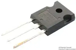


IRGP4620D-EPBF
IGBT, 32 A, 1.55 V, 140 W, 600 V, TO-247AD, 3 Pins
- Manufacturer: INFINEON
- Product type: Single IGBTs
- No. of Pins: 3Pins
- Power Dissipation: 140W
- Transistor Mounting: Through Hole
- Transistor Case Style: TO-247AD
- Operating Temperature Max: 175°C
- Continuous Collector Current: 32A
- Collector Emitter Voltage Max: 600V
- Collector Emitter Saturation Voltage: 1.55V
| Delivery and price | |
|---|---|
| Units per pack | 1 |
| Price | 2.61 € |
| Current stock | 10+ |
| Lead time | 30 days |
IR IGBT IRGB4620DPbF IRGIB4620DPbF IRGP4620D(-E)PbF IRGS4620DPbF **==> picture [538 x 255] intentionally omitted <==** **----- Start of picture text -----**<br> Insulated Gate Bipolar Transistor with Ultrafast Soft Recovery Diode<br>VCES = 600V C C<br>C<br>IC = 20A, TC =100°C<br>tSC ≥ 5µs, TJ(max) = 175°C E<br>C<br>G G C [E ] C [E ]<br>G<br>VCE(ON) typ. = 1.55V @ IC = 12A<br>ao IRGP4620DPbF IRGP4620D-EPbF<br>IRGB4620DPbF<br>TO-247AC TO-247AD<br>TO-220AB<br>C C<br>Applications<br>• Industrial Motor Drive<br>• Inverters<br>E C [E ]<br>• UPS G G C G<br>• Welding<br>E IRGIB4620DPbF IRGS4620DPbF<br>n-channel TO-220AB Full-Pak D [2] Pak<br>**----- End of picture text -----**<br> G C E Gate Collector Emitter ~~————~~ |**Features**<br>**Benefits**<br>Low VCE(ON)and switching losses<br>High efficiency in a wide range of applications and switching<br>frequencies<br>Square RBSOA and maximum junction temperature 175°CImproved reliability due to rugged hard switching<br>performance and high power capability<br>Positive VCE(ON)temperature coefficient<br>Excellent current sharinginparallel operation<br>5µs Short Circuit SOA<br>Enables short circuit protection scheme<br>Lead-Free, RoHS Compliant<br>Environmentally friendly<br>~~——_——~~<br>~~ee~~<br>~~DR~~<br>~~_——————~~| |---| |**Base part number**<br>**Package Type**<br>**Standard Pack**<br>**Orderable Part Number**| |**Form**<br>**Quantity**| |IRGB4620DPbF<br>TO-220AB<br>Tube<br>50<br>IRGB4620DPbF| |IRGIB4620DPbF<br>TO-220AB Full-Pak<br>Tube<br>50<br>IRGIB4620DPbF| |IRGP4620DPbF<br>TO-247AC<br>Tube<br>25<br>IRGP4620DPbF| |IRGP4620D-EPbF<br>TO-247AD<br>Tube<br>25<br>IRGP4620D-EPbF| |Tube<br>50<br>IRGS4620DPbF| |IRGS4620DPbF<br>D2Pak<br>Tape and Reel Right<br>800<br>IRGS4620DTRRPbF| |Tape and Reel Left<br>800<br>IRGS4620DTRLPbF| 1 2015-11-23 ~~Cinfin eon~~ |<br>IRGB/IB/P/SP4620D/EPbF<br>**Absolute Maximum Ratings**<br>~~Cinfineon~~<br>~~LLL~~|| |---|---| |**Parameter**<br>**Max.**<br>**Units**<br>VCES<br>Collector-to-Emitter Voltage<br>600<br>V<br>IC @TC= 25°C<br>Continuous Collector Current<br>32<br>A<br>IC@ TC =100°C<br>Continuous Collector Current<br>20<br>ICM<br>Pulse Collector Current, VGE=15V<br>36<br>ILM<br>Clamped Inductive Load Current, VGE=20V<br>48<br>IF @TC= 25°C<br>Diode Continuous Forward Current<br>16<br>IF @TC= 100°C<br>Diode Continuous Forward Current<br>10<br>IFM<br>Diode Maximum Forward Current<br>48<br>~~es~~<br>~~I~~<br>~~es~~<br>~~ee~~<br>~~———~~<br>~~or~~|| |VGE<br>Continuous Gate-to-Emitter Voltage<br>±20<br>V<br>Transient Gate to Emitter Voltage<br>±30<br>~~ee~~|| |PD@ TC =25°C<br>Maximum Power Dissipation<br>140<br>W<br>PD @TC= 100°C<br>Maximum Power Dissipation<br>70<br>~~eS~~|| |TJ<br>Operating Junction and<br>-40 to +175<br>C<br>TSTG<br>Storage Temperature Range<br>Soldering Temperature, for 10 sec. (1.6mm from case)<br>300<br>Mounting Torque, 6-32 or M3 Screw (TO-220, TO-247)<br>10 lbf·in (1.1 N·m)<br>~~a~~<br>~~es~~|| |**Thermal Resistance**|| |**Parameter**<br>**Min.**<br>**Typ.**<br>**Max. Units**<br>~~a RG~~|| |Thermal Resistance Junction-to-Case(D2Pak,TO-220)<br>–––<br>–––<br>1.07<br>°C/W<br>RθCS<br>Thermal Resistance, Case-to-Sink (flat, greased surface-TO-220, D2Pak,<br>TO-220 Full-Pak )<br>–––<br>0.50<br>–––<br>RθJA<br>Thermal Resistance,Junction-to-Ambient(PCB Mount - D2Pak) <br>–––<br>–––<br>40<br>Thermal Resistance Junction-to-Case(D2Pak,TO-220)<br>–––<br>–––<br>3.66<br>Thermal Resistance Junction-to-Case(TO-247)<br>–––<br>–––<br>1.12<br>Thermal Resistance Junction-to-Case(TO-247)<br>–––<br>–––<br>3.71<br>Thermal Resistance,Junction-to-Ambient(Socket Mount –TO-247)<br>–––<br>–––<br>40<br>Thermal Resistance,Junction-to-Ambient(Socket Mount –TO-220)<br>–––<br>–––<br>62<br>RθJC(IGBT)Thermal Resistance Junction-to-Case(TO-220 Full-Pak)<br>–––<br>–––<br>3.75<br>RθJC(Diode)Thermal Resistance Junction-to-Case(TO-220 Full-Pak)<br>–––<br>–––<br>6.22<br>Thermal Resistance Case-to-Sink(TO-247)<br>–––<br>0.24<br>–––<br>Thermal Resistance,Junction-to-Ambient(Socket Mount –TO-220 Full-Pak)<br>–––<br>–––<br>65<br>~~a~~<br>~~————————~~<br>~~ll~~<br>~~Fya~~<br>~~ss~~<br>~~a~~<br>——~~——SSSS=__—————~~|| |**Electrical Characteristics@ TJ = 25°C(unless otherwise specified)**|| |**Parameter**<br>**Min.**<br>**Typ.**<br>**Max.**<br>**Units**<br>**Conditions**<br>V(BR)CES<br>Collector-to-Emitter Breakdown Voltage<br>600<br>—<br>—<br>V<br>VGE =0V, IC =100µA<br>ΔV(BR)CES/ΔTJTemperature Coeff. of Breakdown Voltage<br>—<br>0.40<br>—<br>V/°C VGE= 0V,IC= 1mA(25°C-175°C)<br>VCE(on)<br>Collector-to-Emitter Saturation Voltage<br>—<br>1.55<br>1.85<br>IC =12A, VGE =15V, TJ =25°C<br>—<br>1.90<br>—<br>IC =12A, VGE =15V, TJ =150°C<br>VGE(th)<br>Gate Threshold Voltage<br>4.0<br>—<br>6.5<br>V<br>VCE= VGE,IC= 350µA<br>ΔVGE(th)/ΔTJ<br>Threshold Voltage Temp. Coefficient<br>—<br>-18<br>—<br>mV/°C VCE= VGE,IC= 1.0mA(25°C-175°C)<br>gfe<br>Forward Transconductance<br>—<br>7.7<br>—<br>S<br>VCE =50V, IC =12A, PW=80µs<br>ICES<br>Collector-to-Emitter Leakage Current<br>—<br>2.0<br>—<br>µAVGE =0V, VCE =600V<br>—<br>475<br>—<br>VGE =0V, VCE =600V, TJ =175°C<br>IGES<br>Gate-to-Emitter Leakage Current<br>—<br>—<br>±100<br>nA<br>VGE =±20V<br>VFM<br>Diode Forward Voltage Drop<br>—<br>2.1<br>3.1<br>V<br>IF =12A<br>—<br>1.6<br>—<br>IF =12A, TJ =175°C<br>—<br>1.97<br>—<br>IC= 12A,VGE= 15V,TJ= 175°C<br>V<br>~~es~~<br>~~ID(sD (OU~~<br>~~I~~<br>~~—~~<br>~~ee ee ee Pe~~<br>~~a~~<br>~~——~~<br>~~esRD~~<br>~~(EDQO~~<br>~~ee~~<br>~~ee~~<br>~~2~~<br>~~esnD~~<br>~~(OU~~<br>~~(OU~~<br>~~S(~~O<br>~~a~~<br>~~———~~|| 2 2015-11-23 ## ~~Cinfin eon~~ ## IRGB/IB/P/SP4620D/EPbF ~~LLL~~ ||**Parameter**|**Min.**|**Typ.**<br>~~Oe~~|**Max**<br>~~Oe~~|**Units**<br>~~Oe~~|**Conditions**<br>~~ee~~| |---|---|---|---|---|---|---| |Qg<br>~~——————~~|Total Gate Charge<br>~~——————~~|—<br>~~——————~~|25<br>~~——————~~<br>~~Oe~~|—<br>~~——————~~<br>~~Oe~~|nC<br>~~——————~~<br>~~Oe~~<br>|IC= 12A<br>VGE= 15V<br>VCC= 400V<br>~~————————~~<br>~~ee~~<br>~~oe~~| |g<br>Qge<br>~~——————~~|Gate-to-Emitter Charge<br>~~——————~~|—<br>~~——————~~|7.0<br>~~——————~~<br>~~Oe~~|—<br>~~——————~~<br>~~Oe~~||| |ge<br>Qgc<br>~~——————~~<br>~~oe~~|Gate-to-Collector Charge<br>~~——————~~<br>~~oe~~|—<br>~~——————~~<br>~~oe~~|11<br>~~——————~~<br>~~Oe~~<br>~~oe~~|—<br>~~——————~~<br>~~Oe~~<br>~~oe~~||| |gc<br>Eon<br>~~——————~~<br>~~es~~<br>~~oe~~|Turn-OnSwitchingLoss<br>~~——————~~<br>~~es~~<br>~~oe~~|—<br>~~——————~~<br>~~es~~<br>~~oe~~|75<br>~~——————~~<br>~~Oe~~<br>~~es~~<br>~~oe~~|—<br>~~——————~~<br>~~Oe~~<br>~~es~~<br>~~oe~~|µJ <br>~~——————~~<br>~~Oe~~<br>~~es~~<br>|IC= 12A, VCC= 400V, VGE=15V<br>RG= 22Ω, L = 200µH, LS= 150nH,<br>TJ= 25°C<br>Energy losses include tail & diode<br>reverse recovery<br>~~————————~~<br>~~ee~~<br>~~oe~~<br>~~ee~~| |Eoff<br>~~es~~<br>~~oe~~|Turn-OffSwitchingLoss<br>~~es~~<br>~~oe~~|—<br>~~es~~<br>~~oe~~|225<br>~~es~~<br>~~oe~~|—<br>~~es~~<br>~~oe~~||| |Etotal<br>~~es~~<br>~~oe~~|TotalSwitchingLoss<br>~~es~~<br>~~oe~~|—<br>~~es~~<br>~~oe~~|300<br>~~es~~<br>~~oe~~|—<br>~~es~~<br>~~oe~~||| |td(on)<br>~~oe~~<br>~~are~~|Turn-On delay time<br>~~oe~~<br>~~are~~|—<br>~~oe~~<br>~~are~~|31<br>~~oe~~<br>~~are~~|—<br>~~oe~~<br>~~are~~|ns<br><br>~~are~~|| |d(on)<br>tr<br>~~oe~~<br>~~are~~<br>~~—_~~|Rise time<br>~~oe~~<br>~~are~~<br>~~—_~~|—<br>~~oe~~<br>~~are~~|17<br>~~oe~~<br>~~are~~|—<br>~~oe~~<br>~~are~~||| |td(off)<br>~~oe~~<br>~~are~~<br>~~—_~~|Turn-Off delay time<br>~~oe~~<br>~~are~~<br>~~—_~~|—<br>~~oe~~<br>~~are~~|83<br>~~oe~~<br>~~are~~|—<br>~~oe~~<br>~~are~~||| |d(off)<br>tf<br>~~oe~~<br>~~are~~<br>~~—_~~<br>~~===~~|Fall time<br>~~oe~~<br>~~are~~<br>~~—_~~<br>~~===~~|—<br>~~oe~~<br>~~are~~<br>~~===~~|24<br>~~oe~~<br>~~are~~<br>~~===~~|—<br>~~oe~~<br>~~are~~||| |Eon<br>~~oe~~<br>~~—_~~<br>~~===~~|Turn-On SwitchingLoss<br>~~oe~~<br>~~—_~~<br>~~===~~|—<br>~~oe~~<br>~~===~~|185<br>~~oe~~<br>~~===~~|—<br>~~oe ~~|µJ<br>|IC= 12A, VCC= 400V, VGE=15V<br>RG= 22Ω, L = 200µH, LS= 150nH,<br>TJ= 175°C<br>Energy losses include tail & diode<br>reverse recovery<br> ~~oe~~<br>~~ee~~<br>~~ne~~| |Eoff<br>~~—_~~<br>~~—===~~|Turn-Off Switching Loss<br>~~—_~~<br>~~===~~|—<br>~~===~~|355<br>~~===~~|—||| |Etotal<br>~~—===~~|Total Switching Loss<br>~~===~~|—<br>~~===~~|540<br>~~===~~|—||| |td(on)<br>~~===~~|Turn-On delay time<br>~~===~~|—<br>~~===~~|30<br>~~===~~|—|ns<br>~~Oe~~|| |d(on)<br>tr<br>~~===~~|Rise time<br>~~===~~|—<br>~~===~~|18<br>~~===~~|—||| |td(off)<br>~~===~~|Turn-Off delay time<br>~~===~~|—<br>~~===~~|102<br>~~===~~|—||| |d(off)<br>tf<br>~~===~~<br>~~a~~<br>~~a~~|Fall time<br>~~===~~<br>~~a~~|—<br>~~===~~<br>~~a~~|41<br>~~===~~<br>~~a~~<br>~~Oe~~|—<br>~~a~~<br>~~Oe~~||| |Cies<br>~~===~~<br>~~a~~<br>~~—————————~~<br>~~a~~|Input Capacitance<br>~~===~~<br>~~a~~<br>~~—————————~~|—<br>~~===~~<br>~~a~~<br>~~—————————~~|765<br>~~===~~<br>~~a~~<br>~~—————————~~<br>~~Oe~~|—<br>~~a~~<br>~~—————————~~<br>~~Oe~~|pF<br>~~—————————~~<br>~~Oe~~|VGE= 0V<br>VCC= 30V<br>f = 1.0MHz<br>~~ee~~<br>~~—————————~~<br>~~ne~~| |Coes<br>~~a~~<br>~~—————————~~<br>~~a~~|Output Capacitance<br>~~a~~<br>~~—————————~~|—<br>~~a~~<br>~~—————————~~|52<br>~~a~~<br>~~—————————~~<br>~~Oe~~|—<br>~~a~~<br>~~—————————~~<br>~~Oe~~||| |Cres<br>~~—————————~~<br>~~a~~|Reverse Transfer Capacitance<br>~~—————————~~|—<br>~~—————————~~|23<br>~~—————————~~<br>~~Oe~~|—<br>~~—————————~~<br>~~Oe~~||| |RBSOA<br>~~a~~|Reverse Bias Safe Operating Area|FULL SQUARE<br>~~Oe~~|||~~Oe ~~|TJ= 175°C, IC= 48A<br>VCC= 480V, Vp ≤ 600V<br>RG= 22Ω,VGE= +20V to 0V<br> ~~ne~~| |SCSOA<br>~~a~~|Short Circuit Safe Operating Area<br>|5.0<br><br>~~a~~|—<br>|—<br>|µs <br>|VCC= 400V, Vp ≤ 600V<br>RG= 22Ω,VGE= +15V to 0V<br><br>~~ne~~| |Erec<br>~~————————~~|Reverse Recovery Energy of the Diode<br>~~————————~~|—<br>~~————————~~<br>~~a~~|280<br>~~————————~~|—<br>~~————————~~|µJ<br>~~————————~~|TJ= 175°C<br>VCC= 400V, IF= 12A, VGE= 15V,<br>Rg=22Ω,L=200µH, LS =150nH<br>~~————————~~<br>~~ne~~| |trr<br>~~————————~~|Diode Reverse Recovery Time<br>~~————————~~|—<br>~~————————~~<br>~~a~~|68<br>~~————————~~|—<br>~~————————~~|ns<br>~~————————~~|| |Irr<br>~~————————~~|Peak Reverse RecoveryCurrent<br>~~————————~~|—<br>~~————————~~<br>~~a~~|19<br>~~————————~~|—<br>~~————————~~|A<br>~~————————~~|| - R θ is measured at TJ of approximately 90°C. - Refer to AN-1086 for guidelines for measuring V(BR)CES safely. - Pulse width limited by maximum junction temperature. - Values influenced by parasitic L and C in measurement. - When mounted on 1” square PCB (FR-4 or G-10 Material). For recommended footprint and soldering techniques refer to application note #AN-994.http://www.irf.com/technical-info/appnotes/an-994.pdf - VCC = 80% (VCES), VGE = 20V, L = 100µH, RG = 22Ω. 3 2015-11-23 ## ~~Cinfineon~~ **==> picture [489 x 238] intentionally omitted <==** **----- Start of picture text -----**<br> IRGB/IB/P/SP4620D/EPbF<br>|<br>150<br>125<br>Toon | 100 «Nae<br>PEEPaNaN 75 PSOEaNGne<br>50<br>rR] EESN=<br>25<br>PELE\ FECES<br>\ 0 Pi tL EN<br>50 75 100 125 150 175 25 50 75 100 125 150 175<br> TC (°C) TC (°C)<br>Ptot (W)<br>**----- End of picture text -----**<br> **==> picture [206 x 669] intentionally omitted <==** **----- Start of picture text -----**<br> 40<br>30<br>20 PEEPaNaN<br>10 rR]<br>0 PELE\<br>25 50 75 100 125 150 175<br> TC (°C)<br>Fig. 1 - Maximum DC Collector Current vs.<br>Case Temperature<br>100<br>10µsec<br>10 100µsec<br>1msec<br>1 DC<br>Tc = 25°C<br>Tj = 175°C<br>Single Pulse<br>0.1 a<br>1 10 100 1000<br>VCE (V)<br>Fig. 3 - Forward SOA<br>TC = 25°C; TJ ≤ 175°C; VGE = 15V<br>45<br>40 CCOREOOEOE<br>35 a oS<br>VGE = 18V<br>30<br>VGE = 15V<br>25 TS VGE = 12V<br>VGE = 10V<br>20 aie VGE = 8.0V<br>CHS<br>15 CV eS AE<br>10 SWEAT<br>5 Po<br>0 AS S50<br>0 1 2 3 4 5 6 7 8<br> VCE (V)<br>ICE (A)<br>IC (A)<br>IC (A)<br>**----- End of picture text -----**<br> **Fig. 2** - Power Dissipation vs. **Fig. 1** - Maximum DC Collector Current vs. **Fig. 2** Case Temperature Case Temperature **==> picture [206 x 435] intentionally omitted <==** **----- Start of picture text -----**<br> 100<br>10<br>1 ee<br>10 100 1000<br>VCE (V)<br>Fig. 4 - Reverse Bias SOA<br>TJ = 175°C; VGE = 20V<br>45<br>40 LT<br>35 CRS V GE = 18V<br>VGE = 15V<br>30 VGE = 12V<br>VGE = 10V<br>25 COW VGE = 8.0V<br>7 oon<br>20 iy Anaya<br>15 ALOE<br>10 n/a<br>5 WEE<br>0 aL ELCIee<br>0 1 2 3 4 5 6 7 8<br> VCE (V)<br>ICE (A)<br>IC (A)<br>**----- End of picture text -----**<br> **Fig. 5** - Typ. IGBT Output Characteristics **Fig. 6** - Typ. IGBT Output Characteristics TJ = -40°C; tp = 80µs TJ = 25°C; tp = 80µs 4 2015-11-23 ~~re~~ IRGB/IB/P/SP4620D/EPbF ~~ee~~ ## ~~Cinfineon~~ **==> picture [544 x 732] intentionally omitted <==** **----- Start of picture text -----**<br> 45 80<br>40 V GE = 18V > Ann > [1<br>70<br>VGE = 15V<br>35 VGE = 12V<br>VGE = 10V AT 60 a<br>30 VGE = 8.0V Re a -40°c a<br>50<br>25°C<br>25<br>175°C<br>40<br>20 Pt TL PAN TL wy,<br>15 ART 30 n/n<br>10 20<br>5 ae2 ZeerT oT 10 a a Ye=|<br>0 ALEC AA<br>0<br>0 1 2 3 4 5 6 7 8<br>0.0 1.0 2.0 3.0 4.0<br> VCE (V) VF (V)<br>Fig. 7 - Typ. IGBT Output Characteristics Fig. 8 - Typ. Diode Forward Voltage Drop<br>TJ = 175°C; tp = 80µs Characteristics<br>2018 a 2018 a<br>16 |} 16 ae ee ee<br>14 14<br>12 tho I CE = 6.0A 12 teh I CE = 6.0A<br>10 i ICE = 12A 10 | ICE = 12A<br>8 I CE = 24A 8 I CE = 24A<br>mes aco<br>64 mistaee a 64 Rmiaeaa a<br>2 ae A ee 2 PWR<br>0 es ee 0 es<br>5 10 15 20 5 10 15 20<br> VGE (V) VGE (V)<br>Fig. 9 - Typical VCE vs. VGE Fig. 10 - Typical VCE vs. VGE<br>TJ = -40°C TJ = 25°C<br>2018 eeee 50<br>T = 25°C<br>J<br>16 ee 40 S| T = 175°C wa<br>J<br>14<br>12 FA I CE = 6.0A 30 i) a<br>10 HH ICE = 12A J<br>8 Ee I CE = 24A 20 i a<br>6<br>4 HA 10 | fe<br>2 ee V<br>0 0<br>5 10 15 20 0 5 10 15<br> VGE (V) VGE (V)<br>Fig. 11 - Typical VCE vs. VGE Fig. 12 - Typ. Transfer Characteristics<br>TJ = 175°C VCE = 50V; tp = 10µs<br>5 2015-11-23<br>re<br>ICE (A)<br>ICE (A)<br>VCE (V) VCE (V)<br>IF (A)<br>VCE (V)<br>**----- End of picture text -----**<br> IRGB/IB/P/SP4620D/EPbF ~~LLL~~ ## ~~Cinfineon~~ **==> picture [199 x 196] intentionally omitted <==** **----- Start of picture text -----**<br> 800<br>700<br>600<br>500 EOFF<br>400<br>300 EON<br>200<br>100<br>0<br>0 10 20 30<br>IC (A)<br>Energy (µJ)<br>**----- End of picture text -----**<br> **Fig. 13** - Typ. Energy Loss vs. IC TJ = 175°C; L = 200µH; VCE = 400V, RG = 22 Ω ; VGE = 15V **==> picture [202 x 197] intentionally omitted <==** **----- Start of picture text -----**<br> 500<br>450<br>400 E OFF<br>350<br>300<br>7|\<br>250 E ON<br>200<br>150<br>100<br>50<br>0 25 50 75 100 125<br>Rg ( Ω )<br>Energy (µJ)<br>**----- End of picture text -----**<br> **Fig. 15** - Typ. Energy Loss vs. RG TJ = 175°C; L = 200µH; VCE = 400V, ICE = 12A; VGE = 15V **==> picture [201 x 195] intentionally omitted <==** **----- Start of picture text -----**<br> 25<br>RG = 10 Ω<br>20<br>RG = 22 Ω<br>15<br>RG = 47 Ω<br>10<br>RG = 100 Ω<br>5<br>0<br>0 10 20 30<br>IF (A)<br>IRR (A)<br>**----- End of picture text -----**<br> **Fig. 17** - Typ. Diode IRR vs. IF TJ = 175°C **==> picture [198 x 196] intentionally omitted <==** **----- Start of picture text -----**<br> 1000<br>td OFF<br>100<br>tF<br>td ON<br>10<br>tR<br>1<br>5 10 15 20 25<br>IC (A)<br>Swiching Time (ns)<br>**----- End of picture text -----**<br> **Fig. 14** - Typ. Switching Time vs. IC TJ = 175°C; L = 200µH; VCE = 400V, RG = 22 Ω ; VGE = 15V **==> picture [205 x 437] intentionally omitted <==** **----- Start of picture text -----**<br> 1000<br>tdOFF<br>|e<br>100<br>tF<br>td ON<br>tR<br>camaPL<br>10<br>0 25 50 75 100 125<br>RG ( Ω )<br>Fig. 16 - Typ. Switching Time vs. RGG<br>= 175°C; L = 200µH; VCE = 400V, ICE = 12A; VCE = 400V, ICE = 12A; V = 400V, ICE = 12A; VCE = 12A; V = 12A; VGE = 15V<br>25<br>20<br>Naan<br>15<br>AEE<br>10<br>ENGR<br>etter<br>5<br>0 25 50 75 100 125<br>RG ( Ω)<br>IRR (A)<br>Swiching Time (ns)<br>**----- End of picture text -----**<br> **Fig. 16** - Typ. Switching Time vs. RGG TJ = 175°C; L = 200µH; VCE = 400V, ICE = 12A; VCE = 400V, ICE = 12A; V = 400V, ICE = 12A; VCE = 12A; V = 12A; VGE = 15V **Fig. 18** - Typ. Diode IRR vs. RG TJ = 175°C 6 2015-11-23 IRGB/IB/P/SP4620D/EPbF ~~LLL~~ ## ~~Cinfin eon~~ **==> picture [544 x 734] intentionally omitted <==** **----- Start of picture text -----**<br> 25 1400<br>1200 | |fe<br>20<br>24A<br>oT] 10 Ω<br>1000<br>15 22 Ω<br>800 47 Ω<br>10 (V4 12A —<br>le]<br>600<br>100 Ω<br>5<br>400 6.0A<br>a nee<br>0 200<br>0 500 1000 1500 0 500 1000 1500<br>diF /dt (A/µs) diF /dt (A/µs)<br>Fig. 19 - Typ. Diode IRR vs. diF/dt Fig. 20 - Typ. Diode QRR vs. diF/dt<br>VCC = 400V; VGE = 15V; IF = 12A; TJ = 175°C VCC = 400V; VGE = 15V; TJ = 175°C<br>400 20 120<br>RG = 10 Ω 18 110<br>350<br>300 ————- RG = 22 Ω 16 I 100<br>14 90<br>250 RG = 47 Ω<br>12 80<br>ft A<br>200 |YT 10 PEN J 70<br>8 60<br>150 TA ot VA<br>RG = 100 Ω 6 50<br>100 is a poNT<br>4 40<br>50<br>2 30<br>es Ft<br>0 a ee ee 0 Ft | [lh hcdt CT 20<br>0 10 20 30 8 10 12 14 16 18<br>IF (A) VGE (V)<br>Fig. 21 - Typ. Diode ERR vs. IF Fig. 22 - VGE vs. Short Circuit Time<br>TJ = 175°C VCC = 400V; TC = 25°C<br>10000 16<br>14 VCES = 300V<br>VCES = 400V<br>12<br>Fy<br>1000 Tih Cies ] TI<br>10<br>Seene ute cs7 <=<br>8<br>6<br>Neen Ty<br>100<br>4<br>Coes<br>2<br>Cres<br>ASESE P ACESOC<br>10 0<br>0 20 40 60 80 100 0 5 10 15 20 25 30<br>VCE (V) Q G, Total Gate Charge (nC)<br>Fig. 23 - Typ. Capacitance vs. VCE Fig. 24 - Typical Gate Charge vs. VGE<br> VGE= 0V; f = 1MHz ICE = 12A; L = 600µH<br>7 2015-11-23<br>re<br>Time (µs)<br>Capacitance (pF)<br>Energy (µJ)<br>IRR (A)<br>VGE, Gate-to-Emitter Voltage (V)<br>QRR (µC)<br>Current (A)<br>**----- End of picture text -----**<br> IRGB/IB/P/SP4620D/EPbF ~~EEE~~ ## —. ~~Gt~~ **==> picture [440 x 533] intentionally omitted <==** **----- Start of picture text -----**<br> 10<br>1<br>D = 0.50<br>0.20<br>0.1 Po 0.050.02 0.10 MCCA eee τ J τ ee J τ 1 τ 1 R 1 R1 τ TTT 2 τ R 22 R2 R τ 3 3R τ 3 3 ee τ C | τ C LUT Ri (°C/W) 0.358 0.424 LU 0.000171 0.001361 τ i (sec)<br>0.01 Ci= Ci= τ i / τ Ri i / Ri 0.287 0.009475<br>0.01 SINGLE PULSE<br>( THERMAL RESPONSE ) Notes:<br>1. Duty Factor D = t1/t2<br>2. Peak Tj = P dm x Zthjc + Tc<br>=Cellier 4 st==UMMA<br>0.001<br>1E-006 1E-005 0.0001 0.001 0.01 0.1 1<br>t1 , Rectangular Pulse Duration (sec)<br>Fig. 25 - Maximum Transient Thermal Impedance, Junction-to-Case (IGBT-TO-220Pak)<br>10<br>D = 0.50 LL<br>1<br>0.20<br>rg fimamarisee<br>0.10<br>= 0.05 —Z ttl<br>0.1 | | 0.02 eer SAUL R 1R1 R 2R2 R 3R3 ETTeee Ri (°C/W) ae τ i (sec)<br>0.01 τ J τ J τ C τ C 0.821094 0.000233<br>τ 1 τ 1 τ 2 τ 2 τ 3 τ 3 1.913817 0.001894<br>0.01 FT (yp SINGLE PULSE Ci= Ci ee τ =i /τ Rii / Ri on 0.926641 0.014711<br>( THERMAL RESPONSE ) Notes:<br>1. Duty Factor D = t1/t2<br>2. Peak Tj = P dm x Zthjc + Tc<br>EA EE =<br>0.001<br>1E-006 1E-005 0.0001 0.001 0.01 0.1 1<br>t1 , Rectangular Pulse Duration (sec)<br> thJC )<br>Thermal Response ( Z<br>Thermal Response ( Z thJC )<br>**----- End of picture text -----**<br> **Fig. 26 -** Maximum Transient Thermal Impedance, Junction-to-Case (DIODE-TO-220Pak) 8 2015-11-23 ~~ee~~ ~~Cinfineon~~ IRGB/IB/P/SP4620D/EPbF ~~LLL~~ **==> picture [264 x 58] intentionally omitted <==** **----- Start of picture text -----**<br> L<br>DUT VCC<br>0<br>1K<br>**----- End of picture text -----**<br> **Fig.C.T.1** - Gate Charge Circuit (turn-off) **==> picture [95 x 127] intentionally omitted <==** **----- Start of picture text -----**<br> 4X<br>DC VCC<br>DUT<br>RSH<br>**----- End of picture text -----**<br> **Fig.C.T.3** - S.C. SOA Circuit **==> picture [171 x 100] intentionally omitted <==** **----- Start of picture text -----**<br> R = [VCC]<br>ICM<br>VCC<br>DUT<br>Rg<br>**----- End of picture text -----**<br> **==> picture [202 x 106] intentionally omitted <==** **----- Start of picture text -----**<br> L<br>80 V +<br>- DUT VCC<br>Rg<br>**----- End of picture text -----**<br> **Fig.C.T.2** - RBSOA Circuit **==> picture [223 x 135] intentionally omitted <==** **----- Start of picture text -----**<br> diode clamp /<br>DUT<br>L<br>><br>-5V<br>DUT /<br>VCC<br>DRIVER :<br>Rg<br>**----- End of picture text -----**<br> **Fig.C.T.4** - Switching Loss Circuit **==> picture [190 x 167] intentionally omitted <==** **----- Start of picture text -----**<br> C force<br>100K<br>D1 22K<br>C sense<br>DUT<br>G force 0.0075µF<br>E sense<br>E force<br>**----- End of picture text -----**<br> **Fig.C.T.5** - Resistive Load Circuit **Fig.C.T.6** - BVCES Filter Circuit 9 2015-11-23 ~~re~~ IRGB/IB/P/SP4620D/EPbF **==> picture [510 x 258] intentionally omitted <==** **----- Start of picture text -----**<br> 500 25 500 50<br>400 20 400 40<br>tr<br>300 15 300 30<br>pf pe<br>tf<br>90% ICE TEST<br>200 10 200 90% test 20<br>5% ICE<br>an Wo<br>100 5 100 10<br>10% test current<br>ee \\<br>5% VCE 5% VCE<br>0 0 0 0<br>EOFF Loss EON<br>-100 to -5 -100 -10<br>-0.50 0.50 1.50 11.70 11.90 12.10<br>Time(µs) Time (µs)<br> (V) (A) (V) (A)<br>VCE ICE VCE ICE<br>**----- End of picture text -----**<br> **Fig. WF1** - Typ. Turn-off Loss Waveform @ TJ = 175°C using Fig. CT.4 **Fig. WF2** - Typ. Turn-on Loss Waveform @ TJ = 175°C using Fig. CT.4 **==> picture [172 x 264] intentionally omitted <==** **----- Start of picture text -----**<br> 25<br>20<br>QRR<br>15<br>tRR<br>10<br>5<br>0<br>-5 10%<br>Peak<br>Peak<br>-10 I RR I RR<br>-15<br>-20<br>-25<br>-0.05 0.05 0.15<br>time (µS)<br> (A)<br>RR<br>I<br>**----- End of picture text -----**<br> **==> picture [209 x 262] intentionally omitted <==** **----- Start of picture text -----**<br> 500 250<br>400 200<br>VCE<br>300 150<br>ICE<br>200 100<br>100 50<br>0 0<br>-100 -50<br>-5.00 0.00 5.00 10.00<br>time (µS)<br> (V) (A)<br>CE CE<br>V I<br>**----- End of picture text -----**<br> **Fig. WF3** - Typ. Diode Recovery Waveform @ TJ = 175°C using Fig. CT.4 **Fig. WF4** - Typ. S.C. Waveform @ TJ = 150°C using Fig. CT.3 10 2015-11-23 ~~Cinfineon~~ IRGB/IB/P/SP4620D/EPbF ~~LLL~~ ## TO-220AB Package Outline (Dimensions are shown in millimeters (inches)) ## TO-220AB Part Marking Information E X A M P L E : T H IS IS A N IR F 1 0 1 0 L O T C O D E 1 7 8 9 A S S E M B L E D O N W W 1 9 , 2 0 0 0 IN T H E A S S E M B L Y L IN E "C " N o t e : "Pin" ind ic aa t es sse "Lm eb aly lind - Fe pr e oe "s it io n **==> picture [219 x 69] intentionally omitted <==** **----- Start of picture text -----**<br> P A R T N U M B E R<br>IN T E R N A T IO N A L<br>R E C T IF IE R<br>L O G O<br>D A T E C O D E<br>Y E A R 0 = 2 0 0 0<br>A S S E M B L Y<br>L O T C O D E W E E K 1 9<br>L IN E C<br>**----- End of picture text -----**<br> TO-220AB package is not recommended for Surface Mount Application. 11 2015-11-23 ~~Cinfineon~~ IRGB/IB/P/SP4620D/EPbF ~~_.......~~ ## TO-220AB Full– Pak Package Outline (Dimensions are shown in millimeters (inches)) ## TO-220AB Full– Pak Part Marking Information TO-220AB Full-Pak package is not recommended for Surface Mount Application. 12 2015-11-23 ~~Cinfineon~~ IRGB/IB/P/SP4620D/EPbF ~~LLL~~ ## TO-247AC Package Outline Dimensions are shown in millimeters (inches) ## TO-247AC Part Marking Information ## Notes: This part marking information applies to devices produced after 02/26/2001 **==> picture [454 x 98] intentionally omitted <==** **----- Start of picture text -----**<br> EXAMPLE: THIS IS AN IRFPE30<br>WITH ASSEMBLY PART NUMBER<br>LOT CODE 5657 INTERNATIONAL pen<br>ASSEMBLED ON WW 35, 2001 RECTIFIER IRFPE30<br>LOGO 135H<br>IN THE ASSEMBLY LINE "H"<br>P re 56 57<br>DATE CODE<br>ASSEMBLY YEAR 1 = 2001<br>Note: "P" in assembly line position<br>LOT CODE WEEK 35<br>indicates "Lead-Free"<br>LINE H<br>**----- End of picture text -----**<br> TO-247AC package is not recommended for Surface Mount Application. 13 2015-11-23 ~~Cinfineon~~ IRGB/IB/P/SP4620D/EPbF ~~LLL~~ ## TO-247AD Package Outline Dimensions are shown in millimeters (inches) ## TO-247AD Part Marking Information E X A M P L E : T H IS IS A N IR G P 3 0 B 1 2 0 K D -E W IT H A S S E M B L Y L O T C O D E 5 6 5 7 A S S E M B L E D O N W W 3 5 , 2 0 0 0 IN T H E A S S E M B L Y L IN E "H " N o te : "P " in a s s e m b ly lin e p o s itio n in d ic a te s "L e a d -F re e " **==> picture [209 x 81] intentionally omitted <==** **----- Start of picture text -----**<br> P A R T N U M B E R<br>IN T E R N A T IO N A L<br>R E C T IF IE R<br>L O G O Repeer 0 3 5 H anoe |<br>5 6 5 7<br>D A T E C O D E<br>A S S E M B L Y YE A R 0 = 2 0 0 0<br>L O T C O D E W E E K 3 5<br>L IN E H<br>**----- End of picture text -----**<br> TO-247AD package is not recommended for Surface Mount Application. 14 2015-11-23 ~~Cinfineon~~ IRGB/IB/P/SP4620D/EPbF ~~LLL~~ ## D[2] -PAK (TO-263AB) Package Outline Dimensions are shown in millimeters (inches) ## D[2] -Pak (TO-263AB) Part Marking Information **==> picture [311 x 200] intentionally omitted <==** **----- Start of picture text -----**<br> THIS IS AN IRF530S WITH<br>PART NUMBER<br>LOT CODE 8024 INTERNATIONAL C c<br>ASSEMBLED ON WW 02, 2000 RECTIFIER F530S<br>IN THE ASSEMBLY LINE "L" LOGO<br>DATE CODE<br>YEAR 0 = 2000<br>ASSEMBLY (Ju<br>LOT CODE WEEK 02<br>HH<br>LINE L<br>OR<br>PART NUMBER<br>INTERNATIONAL<br>RECTIFIER F530S<br>LOGO DATE CODE<br>P = DESIGNATES LEAD - FREE<br>on PRODUCT (OPTIONAL)<br>ASSEMBLY<br>YEAR 0 = 2000<br>LOT CODE<br>WEEK 02<br>A = ASSEMBLY SITE CODE<br>**----- End of picture text -----**<br> 15 2015-11-23 ~~Cinfineon~~ IRGB/IB/P/SP4620D/EPbF ~~LLL~~ ## D[2] Pak Tape & Reel Information (Dimensions are shown in millimeters (inches)) **==> picture [19 x 6] intentionally omitted <==** **----- Start of picture text -----**<br> TRR<br>**----- End of picture text -----**<br> **==> picture [420 x 142] intentionally omitted <==** **----- Start of picture text -----**<br> 1.60 (.063)<br>1.50 (.059)<br>1.60 (.063)<br>4.10 (.161)<br>3.90 (.153) 1.50 (.059) 0.368 (.0145)<br>0.342 (.0135)<br>FEED DIRECTION 1.85 (.073) 11.60 (.457)<br>1.65 (.065) 11.40 (.449) 24.30 (.957)<br>15.42 (.609)<br>23.90 (.941)<br>15.22 (.601)<br>TRL<br>1.75 (.069)<br>10.90 (.429) 1.25 (.049)<br>10.70 (.421) 4.72 (.136)<br>16.10 (.634) 4.52 (.178)<br>15.90 (.626)<br>**----- End of picture text -----**<br> FEED DIRECTION **==> picture [355 x 185] intentionally omitted <==** **----- Start of picture text -----**<br> 13.50 (.532) 27.40 (1.079)<br>12.80 (.504) 23.90 (.941)<br>4<br>330.00 60.00 (2.362)<br>(14.173) MIN.<br> MAX.<br>30.40 (1.197)<br> MAX.<br>26.40 (1.039) 4<br>24.40 (.961)<br>3<br>**----- End of picture text -----**<br> NOTES : 1. COMFORMS TO EIA-418. 2. CONTROLLING DIMENSION: MILLIMETER. 3. DIMENSION MEASURED @ HUB. 4. INCLUDES FLANGE DISTORTION @ OUTER EDGE. 16 2015-11-23 IRGB/IB/P/SP4620D/EPbF ~~LLL~~ IRGB/IB/P/SP4620D/EPbF ~~Cinfineon LLL~~ **Qualification Information[† ] Qualification Level** Industrial (per JEDEC JESD47F)[†† ] TO-220AB TO-220AB-Full-Pak N/A **Moisture Sensitivity Level** TO-247AC TO-247AD D[2] Pak MSL1 **RoHS Compliant** Yes ~~oa~~ † Qualification standards can be found at International Rectifier’s web site: http://www.irf.com/product-info/reliability/ †† Applicable version of JEDEC standard at the time of product release. **Published by Infineon Technologies AG 81726 München, Germany © Infineon Technologies AG 2015 All Rights Reserved.** ## **IMPORTANT NOTICE** The information given in this document shall in no event be regarded as a guarantee of conditions or characteristics (“Beschaffenheitsgarantie”). With respect to any examples, hints or any typical values stated herein and/or any information regarding the application of the product, Infineon Technologies hereby disclaims any and all warranties and liabilities of any kind, including without limitation warranties of non-infringement of intellectual property rights of any third party. In addition, any information given in this document is subject to customer’s compliance with its obligations stated in this document and any applicable legal requirements, norms and standards concerning customer’s products and any use of the product of Infineon Technologies in customer’s applications. The data contained in this document is exclusively intended for technically trained staff. It is the responsibility of customer’s technical departments to evaluate the suitability of the product for the intended application and the completeness of the product information given in this document with respect to such application. For further information on the product, technology, delivery terms and conditions and prices please contact your nearest Infineon Technologies office (www.infineon.com). ## **WARNINGS** Due to technical requirements products may contain dangerous substances. For information on the types in question please contact your nearest Infineon Technologies office. Except as otherwise explicitly approved by Infineon Technologies in a written document signed by authorized representatives of Infineon Technologies, Infineon Technologies’ products may not be used in any applications where a failure of the product or any consequences of the use thereof can reasonably be expected to result in personal injury. 17 2015-11-23
Updated at February 9, 2023
Infineon Technologies is a globally recognized leader in semiconductor solutions, renowned for driving innovation in power management, energy efficiency, and modern mobility. With a strong legacy of engineering excellence, the company provides highly reliable components designed to meet the rigorous demands of industrial, automotive, and advanced commercial applications. The core of our Infineon portfolio is centered on their industry-leading discrete semiconductors. We offer an extensive selection of single and dual MOSFETs, alongside a robust range of single IGBTs and advanced IGBT modules. These flagship power transistors are essential for high-efficiency power conversion and motor control, providing engineers with superior thermal performance and minimized switching losses. Beyond advanced field-effect transistors, the selection includes a comprehensive array of diodes and rectifiers, heavily featuring Schottky diodes, as well as fast-recovery and RF/PIN diodes. This power foundation is further supported by bipolar transistors, intelligent power modules, and thyristor SCR modules, delivering the critical building blocks required for complex power system designs. To support broader system integration, the portfolio also encompasses specialized solutions such as solid-state relays, AC/DC LED driver ICs, and Bluetooth communications modules. From high-power industrial rectifiers to wireless connectivity adapters, Infineon equips designers with the precision components needed to build efficient, scalable, and fully connected electronic systems.
About Novapart
Novapart is a B2B electronic component broker specialising in stock shortages and cost reduction. We source hard-to-find parts and identify compliant alternatives across a catalogue of 410,000+ components from 500+ manufacturers.
Learn more →Stock Shortage Specialist
When a component is unavailable, discontinued or has an unacceptable lead time, we tap into our network of vetted European and Asian distributors to source what you need — without compromising on quality or traceability.
Request a quote →Compliant Alternatives
We identify pin-to-pin, electrically equivalent substitutes that meet the same certifications (RoHS, AEC-Q100, REACH) as your original specification — validated against datasheets, not just part numbers. Often at a lower cost.
BOM Analysis service →